Winter College on Optics and Energy February Anti-reflection and light-trapping. D. Bagnall Southampton University U.K.
|
|
|
- Adam Shaw
- 5 years ago
- Views:
Transcription
1 212-7 Winter College on Optics and Energy 8-19 February 2010 Anti-reflection and light-trapping D. Bagnall Southampton University U.K.
2 Anti reflection and light trapping Professor Darren Bagnall Electronics and Computer Science, Southampton University
3 Contents Introduction Antireflection Single layer AR coatings Double layer AR coatings Micron-scale texturing Sub-wavelength texturing Light-Trapping texturing plasmonic photonic

4 Challenge of Broadband laser based photonic technologies can be 99.9% efficient over 100nm spectral range applying photonics to photovoltaics requires efficiency for 700nm of bandwidth. optimal solutions for AR and LT require spectral irradiance and IQE to be considered and dissordered (chirped) designs.
5 Biomimetics and Plasmonics colour transparent white
6 Anti reflection


7 Single layer AR coating to reduce reflection a single thin film of quarter wavelength thickness (taking into account refractive index) uses interference to reduce intensity of reflected beem about 110nm of SiO 2 is simplest AR coating for Si
8 Single layer AR coating single layer ARCs are much better than bare surface (roughly half reflection) still, around 20% of light is still reflected
9 Double-layer AR coatings CeO SLAR ZnS,MgF 2 DLAR Double layer coatings can be used to broaden the AR effect and further reduce reflected intensity Ultimately there is only a small range of suitable materials (n) that do not absorb.

10 Double-layer AR coatings [Boden and Bagnall, Prog. Photovolt: Res. Appl. 2009; 17: ]
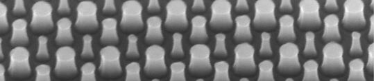
11 Biomimetic moth-eyes Nanostructured corneal surface of some night moths Improved eyesight Less visible to predators Bernhard, Endeavour vol 26, pp , (1967) Arrays of subwavelength features Gradual change in refractive index from air into substrate


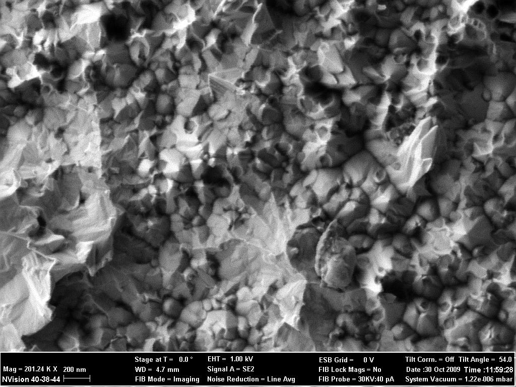
12 Micron-scale texturing micron scale themes are based on the development of topographies that provide light with multiple opportunities to be absorbed reflectance can be as low as 1 2% easy to apply to C Si (KOH etch) difficult to apply to other materials and thin materials (2 um)
 Arrays of subwavelength features Gradual change in refractive")
13 Biomimetic moth-eyes Bernhard, Endeavour vol 26, pp , (1967) Arrays of subwavelength features Gradual change in refractive index from air into substrate

14 Biomimetic moth-eyes sub wavelength patterning creates a gradual change in refractive index and reduces reflection seen on moth eyes our first structures were fabricated by e beam and plasma etch first experimental results illustrates very low reflectance and evidence of structure that can not be explained by effective medium theory


15 Biomimetic moth-eyes CeO SLAR ZnS,MgF 2 DLAR Moth-eye 250 nm Moth-eye 500 nm


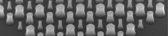
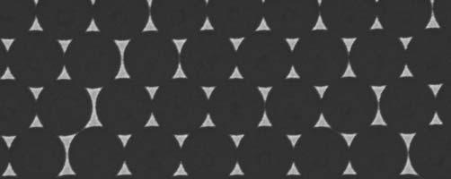
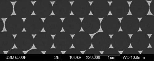
16 Tunable moth-eyes changing height, shape and period of pillar profiles on the reflectance of silicon moth eye arrays. Study reveals a low reflectance band which shifts with array period. samples by nano imprint lithography


17 Biomimetic moth-eyes Pillar shape also has a dramatic effect on the reflectance properties. For highest performance pillar height, shape and array period should be optimized for the specific wavelength range of interest.

18 Design Detail...Period Reflectance with period/wavelength (400nm height)
19 Biomimetic moth-eyes Optimise periodicity by considering: R(λ) QE (λ)and AM1.5(λ)


20 Design Detail...Period Reflectance with period/wavelength (400nm height) S. A. Boden and D. M. Bagnall, Applied Physics Letters, 9, 1108 (2008)


21 Sub-wavelength A/R moth eye AR schemes are promising for thin film solar cells requires self assembly/cheap fabrication nanoscale roughened surfaces might already be doing the job for some thin films

22 Other biomimetics Meanwhile, many other natural systems offer interesting prospects Each represents considerable challenge to fabricate or model colour transparent white
23 Light trapping
24 The case for light-trapping light-trapping can help all devices (enhance absorption or carrier collection, use less material) For a-si, p-si light-trapping is essential but can it be improved?
25 Classic solutions ensure reflection from the back surface of the solar cell (doubles the effective path but in the highly symmetric scheme remaining light is decoupled at surface asymmetric back-reflector ensures multiple reflections (but hard to manufacture) R. H. Morf, in Diffractive Optics for Industrial and Commercial Applications, edited by Jari Turunen and Frank Wyrowski, Akademie Verlag GmbH, Berlin (1997) p61-89 diffuse scattering schemes can increase path-lengths by as much as 20x, but with some escape-cone losses


26 Light-trapping mechanisms Texturing (Lambertian scattering) Periodic structures (diffraction, photonics) Plasmonic (preferential scattering)

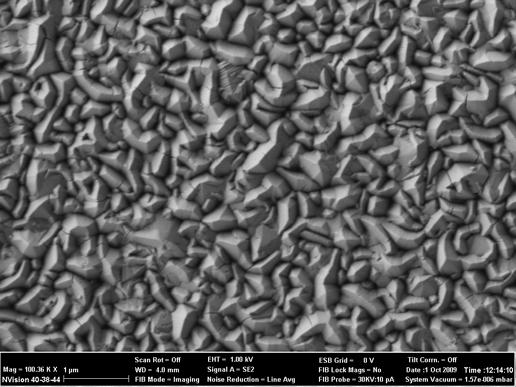
27 Textured Surface Asahi type-u TCO Asahi type-w TCO [N.Taneda, T. Oyama and K. Sato, Proceedings of Intenational PVSEC-17, 2007] Textured TCO on glass can be readily provided by appropriate growth or etching regime Asahi U type is commercial product for a-si devices Required to provide optimum scattering nm wavelengths Classically measured by haze value
28 Lambertian Scattering I = k diffuse d I light cosθ θ θ θ LAMBERTIAN DIFFUSE REFLECTOR Incoming light is scattered equally in all directions Viewed brightness is independent of viewing direction Brightness does depend on direction of illumination
29 Light-trapping air Si LAMBERTIAN DIFFUSE REFLECTOR Fraction of light reflected by total internal reflection = 1 1 n 2 For Si, n=.4. Therefore, 91% of light is reflected back into the cell each time it reaches the top surface escape cone losses account for 9% Overall, the path length can be increased by about a factor of 50

30 Textured TCOs Asahi U type
31 White-light angular scattering Asahi U type -5 Wavelength (nm) Angle (θ) -9
 800 700 600-6 -7-8 500 0 20 40 60")
32 Feature size dependence The main problem with texturing is that long-wavelength scattering requires large feature size Large features sizes are difficult to grow on Commercial designs represent a compromise between optical performance and device performance Asahi U-Type is used for a-si Rougher surfaces are required for micromorph devices -5 Wavelength (nm) Angle (θ) -9

33 Light-trapping for longer wavelengths Asahi type-w TCO [N.Taneda, T. Oyama and K. Sato, Proceedings of Intenational PVSEC-17, 2007] Can metal nanoparticles offer an alternative scattering mechanism?


34 White-light angular scattering EPV 86
35 White-light angular scattering Asahi U type EPV Wavelength (nm) Wavelength (nm) Angle (θ) Angle (θ) -9
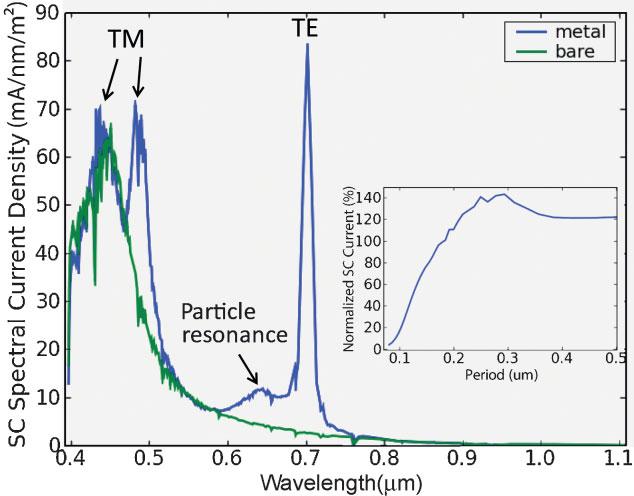
36 Plasmonic Light trapping Can metal nanoparticles offer an alternative scattering mechanism?


37 Plasmonic light-trapping The interaction of light with metal nanoparticles can lead to the generation of localised surface plasmons (LSP). Scattered Incident Transmitted Absorbed Scattered Extinction = Scattering + Absorption
38 Simulations Spheres : Mie theory codes (BHMIE and BHCOAT) (Bohren and Huffmen) Spheroids : Separation of variables (SVM) (Voshchinnikov and Farafonov) Prisms etc : Discrete Dipole Analysis (DDA) (DDSCAT) (Draine and Flatau) (refractive index data taken from Palik)

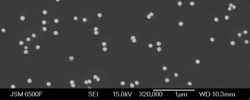
39 Fabrication of metal nanoparticles EBL NSL MIF DFC
 and offer excellent extinction at near")
40 Electron-beam lithography: aspect ratio rectangles can be produced (chemically) and offer excellent extinction at near bandedge

41 Optimized scattering Spheres Spheroids Small particles are highly absorbing, large particles highly scattering Absorption : good for organic, bad for inorganic Scattering : good for all pv (part of light trapping scheme)

42 Choice of metal Qrad > 0.9 Spectrum present at rear of two devices
43 Plasmonic a-si:h solar cells Front Back contact TCO pin a-si TCO with nanopartilces Glass substrate Back Back contact TCO with nanopartilces pin a-si TCO Glass substrate
44 Design Rules You should make sure you : chose a particle size and shape that maximises scattering in the region of low absorption (i.e. the band edge) minimise absorption in the metal across entire spectral range (assuming multiple scattering events small absoprtion will be multiplied 10 fold) select the metal carefully insert the plasmonic layer at the back of the device (short wavelength absorption is unavoidable, avoids surface reflection) use large asymmetric particles as this produces high scattering efficiency at long wavelengths spread the particles about (coupling leads to loss) randomly distribute particles (avoid diffraction) or else take diffraction into account. randomly orientate particles (polarization) or else have vertical & horizontal features understand that your metal nanoparticles change the optical properties of the TCO they sit in (consider reflection and coupling to back contact and antireflection)
45 Conclusions Plasmonic enhancement of an inorganic thin film solar cell has yet to be demonstrated First thin film plasmonic devices will exploit scattering in conjunction with texturing -5-5 Wavelength (nm) Wavelength (nm) Angle (θ) Angle (θ) -9 Enhanced absorption may feature in organic systems (will be harder to use for inorganic) Second generation of inorganic plasmonic devices might utilise preferential scattering and diffraction to allow ultrathin devices
46 Photonic Light trapping
47 Photonic light-trapping We ve looked at random scattering and plasmonic scattering The third light trapping technique could be diffraction Techniques commonly used in photonics for coupling in waveguides We have found that blazed diffraction gratings can be effective (90%) for 200nm spectral range rather expensive to produce for little benefit


48 Photonic light-trapping We ve looked at random scattering and plasmonic scattering The third light trapping technique could be diffraction

49 Plasmonic + Photonic Light trapping

50 Gratings Stanford University

51 Grating Plasmonics Attwater group


52 Conclusions Nanotechnology and photonics increasingly important to PV Challenges are self organised fabrication integration into fabrication sequence reliability reproducibility of nano processes