Center for Integrated Nanotechnologies & Semiconducting Nanowires
|
|
|
- Jared Chapman
- 5 years ago
- Views:
Transcription
1 Center for Integrated Nanotechnologies & Semiconducting Nanowires S. Tom Picraux Chief Scientist Center for Integrated Nanotechnologies Arizona Nanotechnology: Small is Big April 10,


2 Center for Integrated Nanotechnologies Sandia National Laboratories Los Alamos National Laboratory One scientific community focused on nanoscience integration World class scientific staff Vibrant user community State-of-the-art facilities A focused attack on nanoscience integration challenges Leveraging LANL/SNL capabilities Developing and deploying innovative approaches to nanoscale integration 2


3 CINT s focus is on Nanoscience Integration The science of nanomaterials integration Combining diverse nanomaterials together into composite structures across length scales and into nanosystems to discover, understand, and design materials with novel properties and performance. Bifunctional materials Metal Semiconductor Directed assembly Active nanosystems Microtubules + Motor Proteins Co CdSe Nanocomposite materials Nanowire arrays 10,000 element 2D mechanical lattice 10 nm Combining ferromagnetic & semiconducting behavior Nanoscale Nanoscale inhomgeneities Engineered nanocomposites Length scale Switchable metamaterials Micro/Macroscale 500 nm Nanomechanical arrays

4 CINT is one of five Department of Energy Nanoscale Science Research Centers (NSRCs) Center for Nanoscale Materials Argonne National Lab. Molecular Foundry Lawrence Berkeley National Lab. Center for Functional Nanomaterials Brookhaven National Lab. Center for Integrated Nanotechnologies Sandia National Labs. Los Alamos National Lab. Center for Nanophase Materials Sciences Oak Ridge National Lab. 4


5 Nanoscience Integration Challenges address key challenges in integration Energy Transfer How do nanoscale systems detect, transfer, and transduce energy? SEM of actual device 1 mm 1-D tunneling in Double Quantum Wires Emergent Properties What are the collective properties of composite nanoscale systems? 5


6 There is significant synergy across thrusts in the approach to the Energy Transfer Grand Challenge e hω Coulomb interaction doubled current Nanosytems: Efficient separation and transport of electrons and holes in coreshell nanowires. h Eg voltage Nanophotonics: Carrier multiplication in quantum wires and epitaxial QDs. 6 Soft/Bio: Assemblies of synthetic lightharvesting nanomaterials. Theory & Simulation: The description of these processes at the quantum and molecular level.


7 The CINT thrusts approach the Emergent Properties Grand Challenge in diverse ways Nanophotonics: Active electromagnetic metamaterials Nanosystems: Collective phenomena in 2D electron gases 7 Soft/Bio: Nanoscale material assemblies that mimic biological functionality Theory & Simulation: Electronic phase separation, protein folding, magnetic ordering, nanoscale quasiparticle properties

 Nanoscale Electronics, Mechanics & Systems Control of")

 (b) Theory & Simulation of")

8 Science Thrusts provide broad expertise Nanophotonics & Optical Nanomaterials Synthesis, excitation and energy transformations of optically active nanomaterials and collective or emergent electromagnetic phenomena (plasmonics, metamaterials, photonic lattices) Nanoscale Electronics, Mechanics & Systems Control of electronic transport and wavefunctions, and mechanical coupling and properties using nanomaterials and integrated nanosystems Soft, Biological, & Composite Nanomaterials Solution-based materials synthesis and assembly of soft, composite and artificial bio-mimetic nanosystems 1-10 nm (a) (b) Theory & Simulation of Nanoscale Phenomena Assembly, interfacial interactions, and emergent properties of nanoscale systems, including their electronic, magnetic, and optical properties Si surface (c) (d) OTS coating 8


9 Discovery Platforms: Unique User Capabilities For Nanomaterials Research Discovery Platforms = chips that allow Users to: Stimulate Interrogate Exploit nanomaterials in microsystem environments CINT provides the platforms F } d Users provide the materials nanomechanics microfluidics 9 optical, transport CINT instrument packaging

10 Discovery Platforms TM are available for experiments These platforms will evolve, based on CINT scientist and user input. Cantilever Array Platform.5 mm 1.5 mm Electrical Transport & Optical Spectroscopy Platform T sensor bond pads electrodes 0.18 μm lines, gaps Ver. 2 for Quantum computing Post processing: n+ polysilicon gates define by EBL & RIE W bond pads light sensor SiO 2 SiO 2 (2) (1) n+ n+ Si SiN 10


11 New instrumentation is essential for progress in nanoscience integration TEM/SPM Single protein force spectroscopy D single particle tracking In situ tensile tester 11 Nanomanipulation for placement of nanostructures

, Sean Hearne, Alec Talin (SNL)")
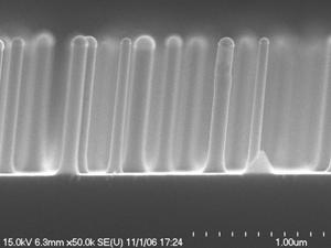
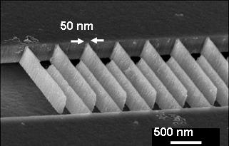
 Nanoimprint-formed Si NWs (b) Al Al Ge NWs Si/Ge axial heterostructured NW (c)")
")
 2 1 NH NH NH Nitrobenzene Phenol NH NH NH NH OH NH NO 2 Future impact National")

12 Nanowires Synthesis, Integration & Applications Semiconductor nanowires will enable previously unattainable control of electronic properties for integrated nanosystems Si, Ge and Si/Ge heterostructure growth CVD NW growth with in situ doping Integration by directed assembly Electrodeposition to embed NWs Tom Picraux (LANL), Sean Hearne, Alec Talin (SNL) Vertical arrays Nanowire sensing Crossbar architecture for high density electronics & sensing (a) Nanoimprint-formed Si NWs (b) Al Al Ge NWs Si/Ge axial heterostructured NW (c) 200μm μm (d) Si NW SiO 2 600nm 200nm Si Assembled planar sensor array ΔV g is proportional to e- donating/withdraing character of analyte molecules (Hammett parameter σ p ) Nitrobenzene, σ p = 0.78 Phenol σ p = -0.7; ΔV g (V) 2 1 NH NH NH Nitrobenzene Phenol NH NH NH NH OH NH NO 2 Future impact National security: ultra sensitive chem/bio sensors; low power electronics Energy applications: high efficiency thermoelectrics Industrial competitiveness: future nanoscale electronic and photonic devices Concentration (M )

 Y/(Y+BEL) 0.6 0.4 0.")

13 NNEDC Project: Nano-electronics and photonics for the 21 st Century Dislocationfree ordered GaN arrays Ordered growth and integration A. Talin GaN and Ge NW devices for electrical/optical characterization modeling contact resistance in nanotubes and nanowires (a) Y/(Y+BEL) Sapphire Resistance (ohm) Leonard & Talin, PRL 97, 2006 State-of-the-art fabrication, test, and modeling of nanodevices Nanoscale circuit simulation 1


14 CINT will play a leading role in nanoscience integration Nanoscience Integration Users Outreach Partnering Science Thrusts Grand Challenges New Tools SNL/LANL Capabilities And Programs 14