On-chip MEMS for automated chip-to-chip assembly
|
|
|
- Drusilla Chapman
- 5 years ago
- Views:
Transcription


1 On-chip MEMS for automated chip-to-chip assembly Dr. Ir. Marcel Tichem, Ir. Tjitte-Jelte Peters, Kai Wu MSc TU Delft, Precision and Microsystems Engineering Photonics Event, Koningshof, Veldhoven, 2 June 2016
,")

2 Photonics for data communication Photonic packages to enable massive data communication Complex packages, containing: Photonic Integrated Circuit (PIC), micro optics, electrical components Integration is a key challenge Technology exists for assembly, however: Labour intensive Expensive 1 st generation 40G package 2


3 Case: multi chip photonic package Fibre Array Unit TriPleX chip Two PICs Multiple O I/O Required precision for each O I/O: 0.1, control,, InP chip LTCC Carrier Courtesy: 3


4 Enabler: microfabrication and MEMS Single fibre Fibre array Passive alignment: geometric mating features Active alignment: use of MEMS


5 The concept Integrate an assembly machine into one of the photonic chips for fine alignment: on chip MEMS Two stage process TriPleX InP Shared substrate Step 1: pre assembly of photonic chips on common carrier, flip chip bonding Peters, Tichem, SPIE Photonics West 2014, doi: / Wörhoff et al, SPIE Photonics Europe, 2016 doi: /

6 The concept Integrate an assembly machine into one of the photonic chips for fine alignment: on chip MEMS The potential: Two stage process Increased assembly automation, cost reduction Local alignment: high precision Step 2: Fine alignment of flexible waveguide structures using on chip MEMS MEMS = MicroElectroMechanical System Peters, Tichem, SPIE Photonics West 2014, doi: / Wörhoff et al, SPIE Photonics Europe, 2016 doi: /

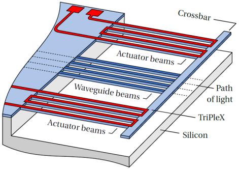
7 On chip functions Functions: Flexible waveguide beams, coupled by cross bar Actuators Waveguide beam locking By on-chip actuators By chip assembly 7
 Design integration All functions cooperating, space consumption Locking precision Maintain")
8 SiO 2 photonic MEMS Challenges Functionality realised in TriPleX material platfor: Fabrication Compressive stress in thick SiO 2 Deformation Residual stress in multi material layers Actuation range All relevant motion direction CTE of SIO 2 (thermal actuators) Design integration All functions cooperating, space consumption Locking precision Maintain position 8
9 Fabrication and results 9
 Peters, Tichem, J. Micromech. Microeng.")
10 Fabrication in TriPleX material platform Frontside release Structuring of photonic layer (plasma etch) Release by underetching Si (isotropic plasma etch) Peters, Tichem, J. Micromech. Microeng. 25 (2015)


11 Fabrication in TriPleX material platform Poor yield SiO 2 under compressive stress Clamped clamped beam situations Peters, Tichem, J. Micromech. Microeng. 25 (2015)
")

12 Fabrication in TriPleX material platform Improved process: Si reinforced 98% yield (single cantilevers) Fabrication process for reliable structure release Peters, Tichem, J. Micromech. Microeng. 25 (2015)


13 Fabrication in TriPleX material platform Improved process: Si reinforced 98% yield (single cantilevers) 18μm 16μm Cantilevers 4-WG beam structure Peters, Tichem, J. Micromech. Microeng. 25 (2015)


14 Thermal bimorph actuators 14


15 Example structure 15


16 16

17 Post fabrication deformation Peters, Tichem, SPIE Photonics Europe, Brussels, 2016, doi / Peters, Tichem, Journal paper under preparation 17


18 Waveguide motion Side view of bimorph actuator 18

19 Motion measurements Peters, Tichem, SPIE Photonics Europe, Brussels, 2016, doi /


20 Height compensation and actuation range using short loop bimorph actuators 20
21 Double-layer membrane A Fully released structures B Initial deflection Bimorph actuators (short loop) Chip150 (short-loop poly-si): L ox =650µm, L h =150µm a b Crossbar Waveguide beams Wu, Tichem, SPIE Photonics West 2016, doi: /

22 Motion measurement Chip150 (short-loop poly-si): Lox=650µm, Lh=150µm Laser vibrometer measurement Amplitude: 4V, Offset: 2V, Frequency: 2Hz Wu, Tichem, SPIE Photonics West 2016, doi: /
23 Conclusions Concept proposed for highly automated, high precision, multi port chip to chip alignment, exploiting MEMS Implementation of concept is challenged by thick ( 16 ) SiO 2 material, and requires smart designs: Reliable fabrication is feasible with proper process design (make use of supportive Si) and chip design (prevent clamped clamped beam situation) Short loop actuator design to use post fabrication deformation for height compensation and have motion ranges in order of few Basic functions demonstrated, currently working on in plane actuation, locking, optical coupling experiments and integration into overall concept 23


24 Towards a complete process EU FP7 PHASTFlex LTCC InP TriPleX Wörhoff et al, SPIE Photonics Europe, 2016 First proof of assembly TriPleX chip w/o MEMS 24


25 Acknowledgement TU Delft co workers Tjitte Jelte Peters, Kai Wu, Alexandre Beck Funding STW GTIP grant 11355, Flex O Guides EU FP7 grant , PHASTFlex, Collaborators from partners, user committee members COBRA 25

26 Thank you