Organic Thin Films Laboratory (OTFL), Hanyang University
|
|
|
- Abraham Barrett
- 5 years ago
- Views:
Transcription
 Department of Chemistry Hanyang University Distinguished Professor Director of Asian Research Network Program President of Asian Research Network Korea Candidate member of the National Academy of")

1 Organic Thin Films Laboratory (OTFL), Hanyang University Prof. Haiwon Lee Department of Chemistry Hanyang University Distinguished Professor Director of Asian Research Network Program President of Asian Research Network Korea Candidate member of the National Academy of Engineering Editor-in-Chief, Nano Convergence Chairman, International Cooperation Promotion Committee, Ministry of Science, ICT and Future Planning (MSIP) Projects Development of Nanostructured Sensor Matrix Based on Signal Amplification for Highly Sensitive Diagnosis of Disease Biomarkers, The Ministry of Science, ICT and Future Planning Template Effect on Guiding Biomolecular Growth by 3-D Carbon Nanotube Networks on Silicon and Quartz Plates, AOARD Development of Energy Storage Functional Nano-Micro One-Dimensional Fiber/Textile Device, Ministry of Science, ICT and Future Planning & Information Technology Research Center University-Centered Labs: Biomimetic Nanosensor Systems, Ministry of Education Collaborations Gwangju Institute of Science and Technology(GIST), Korea Advanced Institute of Science and Technology (KAIST), Korea Institute of Science and Technology(KIST), Sungkyunkwan University(SKKU), Park Systems, National Nanofab Center(NNFC), Tokyo Institute of Technology(TIT), Nanyang Technological University(NTU), Indian Institute of Technology Madras(IITM), University of Pennsylvania(UPENN). Contact & Web Sites Prof. Haiwon Lee: (Asian Research Network)


2 Research Overview at Prof. Haiwon Lee s Lab Applications of CNTs Fabrication & Modification of CNTs AFM characterization and Lithography


3 Research: Synthesis of Carbon Nanotubes (Fabrication & Modification) Various Structures of Grown CNTs Thermal CVD Synthesis of CNts Vertical Alignment 3D Network CNTs curtain Plasma Enhanced CVD CNTs Coated on Various Substrates Al 2 O 3 MnO 4 2μm Synthesis of 3D CNTs Polyaniline Gold 1μm 2μm

4 Research: Applications of CNTs
 b) b) d) c) SEM images of a)")

 The SWCNTs-PDMS film")
 One")


 Reliability of the resistance")
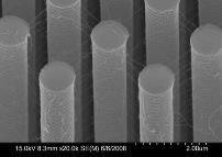
5 Carbon Nanotube Strain Sensors a) a) b) b) d) c) SEM images of a) 3D network of SWCNTs b) Si pillar arrays after removing the 3D network of SWCNTs by a lifting-up process c) The SWCNTs-PDMS film d) Top view SEM image of the 3D network of SWCNTs in PDMS c) One Dimension Two Dimension CNT Strain Sensor Resistance characteristics of the 3D network of SWNTs in PDMS. a) Resistance under an applied tensile strain of 0.5% to 3.0%. b) The relative change in electrical resistance versus mechanical strain. c) Reliability of the resistance under an applied tensile strain of 1.0%. Three Three Dimension Dimension


, and after")
. Fluorescence Microscopic")

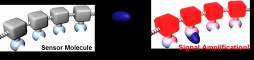
6 3D Networked Polydiacetylene Based Color Sensor Signal Amplification Effect of PDA Vesicles 3D Network of CNTs for PDA Sensor Platform (A D) SEM images of networked CNT (A and B), after Al 2 O 3 deposition (C), and after immobilization of PDA vesicles (D). Fluorescence Microscopic images of the PDA immobilized networked structures from top (E) and side (F) views.


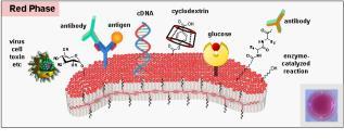


7 Signal Enhancement for Early Diagnosis Anti-body Modified 3D Network Team 1 Team 2 Antibody 3D CNT Network Structure SERS Lap-on-a Chip Signal Amplification Based on Polymers Core Technology Diagnosis, Point-of-Care Phage Display & Aptamer Nano FRET/BRET Micro Biomimetic/Microfluidics Team 3
 2.5 µm spacing and (b, d, f) 5 µm spacing Si pillar templates in microfluidic channel.")
 passing 500 nm green-ps particles through 3D networks on 5 µm spacing Si pillar template, (e) Filtered 500 nm green-ps particles by")
8 3D Network of CNT-Based Biosensor for Cancer Antigen Detection Microfluidic System Based on 3D-Networked CNTs 3D Curtain of CNTs for Biosensor Platform SEM images and optical images of Al 2 O 3 coated 3D network of SWNTs on (a, c, e) 2.5 µm spacing and (b, d, f) 5 µm spacing Si pillar templates in microfluidic channel. (c) Microscopic image of Si micro pillar in microfluidic channel. And fluorescent microscopic images of (d) passing 500 nm green-ps particles through 3D networks on 5 µm spacing Si pillar template, (e) Filtered 500 nm green-ps particles by 3D networks on 2.5 µm spacing template, and (f) filtered 1 µm red-ps particles by 3D networks on 5 µm spacing template. IN A B C OUT


9 Growth of Neuron on 3D Network of cnt-based templates


 pristine Si")
10 Supercapacitor based on 3d network cnt Templates 3D Network of CNTs 5um + Polyaniline 2um - Good electroactivity - Ease of synthesis at low cost - Good processability - Environmental Stability - Doping/de-doping chemistry Schematic illustration of 3DNC/MnOx fabrication process and SEM images of (a) pristine Si pillar substrate, (b) as synthesized 3DNC and (c) 3DNC/MnOx. 300nm
")
 before and (b) after protein immobilization.")


11 Research: AFM Characterization and Lithography AFM Measurement & Recognition Scanning Probe Lithography (c) (d) (a), (b): Tapping mode AFM image of the gold dot array (a) before and (b) after protein immobilization. (c): Non-contact mode AFM image of Micro cyclic diacetylene-3 nanotube. (d): An AFM image showing SWCNTs aligned in the WS-PANI/PVA/SWCNTs nanofiber. Scheme of Line Patterning AFM topography of (a) decompose cobalt pattern after performing lithography and (b) fabricated uniform and well-connected cobalt nanostructures after the development process


12 Laboratory Events Homecoming Day Laboratory Tour Tokyo Institute of Technology Japan Students Visit OTFL Progress Meeting OTFL Picnic OTFL Year-End Party
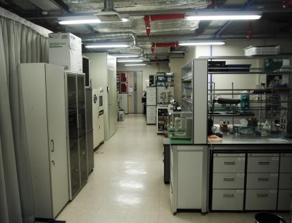

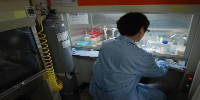
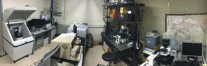


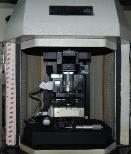


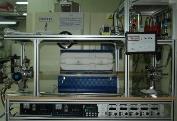
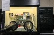
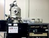
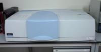

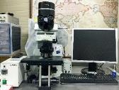

13 Laboratory Environment Laboratory Equipment AFM (XE-100) AFM (XE-100) PE(Plasma-Enhanced) CVD FTC 5th Floor Laboratory Sample Preparation Room Thermal CVD Thermal CVD Thermal Evaporator Glove box UV-O 3 Cleaner UV/VIS/NIR Ellipsometer Fluorescens-Microscope Bio Chamber Measurement Chamber Strain Sensor
 Dongwoo Fine-Chem (8 People) LG (10 People) Samsung (25 People)")
 Research Professor (3 People) ( Hanyang & Korea University ) Ph.")
14 Alumni Status ( ) Other Business (42People) ( SK, Dongjin Semichem, 코오롱, 3M, etc. Hynix (7 People) Dongwoo Fine-Chem (8 People) LG (10 People) Samsung (25 People) Professor (2 People) ( Hanyang & Suwon University ) National Institute Researcher (1 People) Research Professor (3 People) ( Hanyang & Korea University ) Ph.D Student (8 People)