Using new international patented production technologies for polymer mems and high-integrated systems
|
|
|
- Mabel Stevens
- 5 years ago
- Views:
Transcription


1 Using new international patented production technologies for polymer mems and high-integrated systems Micromechanics, MEMS, Plastic Lab-on-a-chip Production Service, Packaging and R&D Advanced Micro- and Nanotechnologies International Patented Technologies: RMPD Rapid Micro Product Development 3D-CSP 3-dimensional Chip Size Packaging From the Idea to the Series Production World Market of MEMS based electronics: 7 Mrd. today, growth >20% per year


2 RMPD - Technologies multimat nanoface mask Assembly parallel stick2 3D-CSP Parallel batch production 300 materials without technology change no tools microfluidic coating with light
3 microtec business today Contract Manufacturing and Contract R&D (licenses and training available for special fields) Micromechanics, MEMS Packaging Services and R&D Services Highly integrated products speed up the need of 3D-packaging technologies. This will become a fast growing market for patented 3D-CSP processes. Customized polymer parts like Lab on a chip, customized series production of polymerchips and components used in industry benefit from international patented RMPD -technologies RMPD Systems are easy to use and easy to maintain =>Fast deliverable series parts in flexible units in high precision at low cost 3D-CSP batch process is fast and cost efficient by parallel connecting pads Easy to handle materials (fluid monomers/polymers) =>no high-risk chemicals Every 3D-CAD Software can be used (*.stl/*.iges/*.step a.s.o) Direct Integration of microelectronic CAD (OrCAD) into Design Simulation and direct series production of multi material systems!


4 Generative processes for microstructures and -systems
5 Parallel batch production by RMPD


6 RMPD -mask batch


7 Typical structure for mass production series production without tooling RMPD -mask allows production runs up to parts per machine and hour Mass production with 5, 9, 14 and 350 mm mask Outlook: 610 mm and RMPD -Rotation


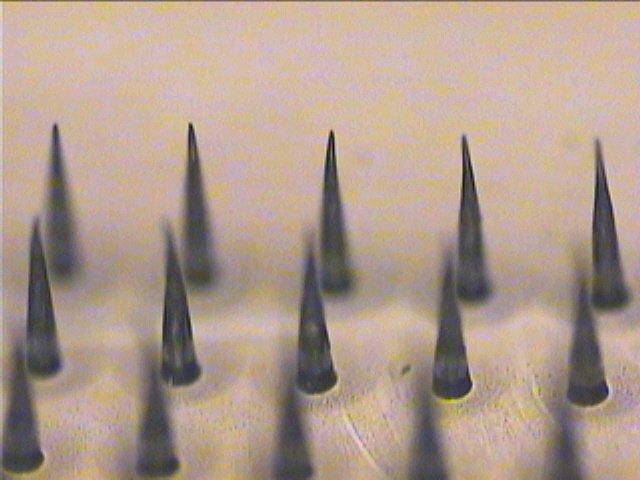
8 High aspect ratio 2006 Anchor tube diameter 200 µm Anchor tube length µm Distance between holes 50 µm 15mm 1997 Anchor tube diameter 150 µm Anchor tube length µm Distance between holes 70 µm


9 Component for Medical Applications, Micro Heat Engines and other applications Nozzle plate for driving head Diameter = 4 mm Nozzle width = 20 µm 20µm


10 Micro-fluidic applications: Intrinsic hydrophilic and hydrophobic material properties require no coating > 90 Hydrophilic materials for: Capillary flow enhancement Hydrophobic material for Dispensing units Nozzle structures Surface protection smart spotting


11 Fluidic- stop structure, as ventilation duct Principle: Gases pass through Liquids are blocked Applications: - Ballpoint pen - Air vent ampule Tube diameter 50 µm Tube length µm Distance between holes 30 µm Aspect ratio 60 3 mm 50µm


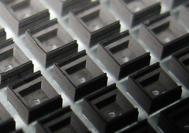
12 Microfludic chips, automaticially processed for analysis Reaction chambers for optical analysis Loading box Ventilation chamber Two different materials in vertical direction Intrinsic hydrophilic and hydrophobic materials


13 3D-CSP NMRC Thermal Simulation Passive cooling: Possible Option: Active cooling via EHD pump


14 3D-CSP RF test structures, RF-parameter available for development of baluns and antennas for ZigBee 25µm Full selected 3D CAD structure Frequency range: 100 MHz 8,5 GHz 4 interconnection - and shielding layers and 6 isolation layers


15 3D-CSP Batch process 5 Zoll, 9 Zoll, 14 Zoll, 350mm Substrat bottom Cavitys 4 Step Process to build MEMS RMPD -Mask Placement of inserts Metallisation Metal Layer structuring


16 3D-CSP Batch process Die`s Pads 4 Step Process to build MEMS RMPD -Mask Placement of inserts Metallisation Metal Layer structuring


17 3D-CSP Batch process Die`s Pads 4 Step Process to build MEMS RMPD -Mask Placement of inserts Metallisation Metal Layer structuring

18 3D-CSP Batch process Metallisation layer 4 Step Process to build MEMS RMPD -Mask Placement of inserts Metallisation Metal Layer structuring

19 3D-CSP Batch process Interconnection layer 4 Step Process to build MEMS RMPD -Mask Placement of inserts Metallisation Metall Layer structuring


20 Sensor with 24-Bit Capacitance to Digital Converter Technology: 3D-CSP with RMPD,special sensor adaptation with low interferences sensor interconnection layer Connected PCB flex circuit 3D-CSP System capacitor die Temperatur sensor on chip resolution 0.1 C Two wire serial interface (I 2 C- compatible)


21 System-in-Package Solutions based on 3D-CSP Only processor and networking subsystem! Intelligent Networked Optical Sensor


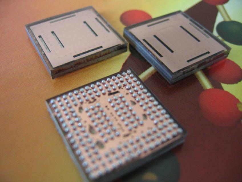
22 3D-CSP die housing for SMD case sizes 0603 and less <= compare with pencil diameter 0,5mm 0,8 mm

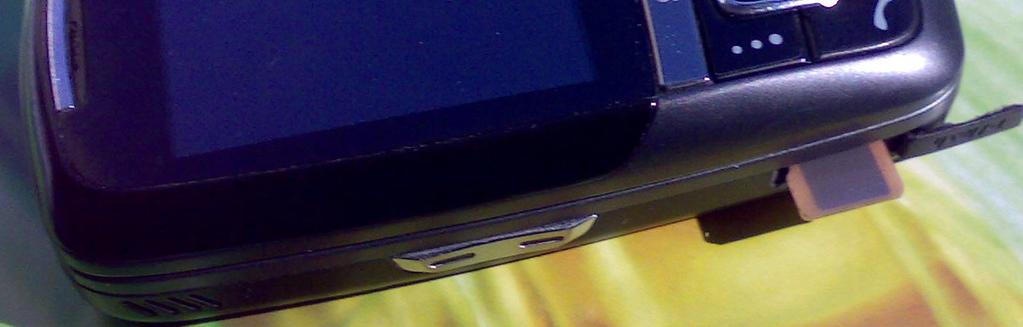


23 3D-CSP application: microsd SMART Card, stack NANDS up to 10 GB
24 Customers Advantages: One stop shop (full service: consulting, R&D, series production) Unique and patented technologies (IP security to customers), microtec technologies and products are protected by patents, some of them are worldwide Capability to integrate market and customer needs very early in product development but without additional costs (CAD to series product) and Speeding up time to market (no tooling) Image and Database: microtec is well known as technology and innovation leader, in 12 years we build up a database of more than 20thousand qualified decision makers with interest in MEMS and nanotechnologies. microtec sales today is focussing 80 companies. Our trademark is international protected too. microtec Website: More than 60thousand visitors from 45 countries every year
25 Organisation Management Accounting R&D Production Sales Office Management: A. Reinhardt, R. Götzen, H. Bohlmann Team: high qualified employees, >50% Engineering degree Shareholder: 48% =IKB Equity Fund I - IKB Deutsche Industriebank AG 52% =(Dr. U. Bittner, Dr. Ing. H. Bohlmann, Dipl. Ing. R. Götzen, A. Reinhardt, Dipl. Ing. J. Rost)
26 Management and Advisory Board Dipl. Ing. Reiner Götzen, CEO/CTO Inventor and founder of microtec. He worked as scientist at University Duisburg, technical designer photo systems at Robot GmbH Düsseldorf and started his career at Thyssen Krupp AG in the field of precision mechanics. Mr. Götzen is working for microtec since 1996 and is the driver of the innovations realized in the last 12 years, particular the international patented production technologies and the customer projects. Andrea Reinhardt, CEO/CFO Educated at University Mannheim she worked in leading position at Real-Film Ludwigshafen and started her career in Banking Citibank Mannheim and DGZ Bank Frankfurt. She is working for microtec since 1996, with focus on business development. Mrs. Reinhardt is co-founder of NTC Nano Tech Coatings GmbH, is active as evaluator for EC and national projects, is part of the European Platform of Micro- and Nanotechnologies MINAM as member of the industrial board and at the public private partnership ZIRP Dr. Ing. Helge Bohlmann, Power of attorney, project manager EC and sales He worked as a scientist at University Hannover, as project manager for IVAM and as sales manager for UBM measuring systems. Dr. Bohlmann is working for microtec since 2000 and is taking care of the EC funded projects and key customers. Advisory Board Dr. Lutz-Dieter Thiele: worked in top management positions at Omron Europa GmbH and Linotype-Hell AG. He is working as management consultant today. Dr. Udo Bittner: worked in management positions at Siemens AG, Start Amadeus ltd, Deutsche Post AG he is now working for Thomas Cook AG in a position of higher management. Dr. Udo Sonnhof, Founder and Managing Director of SPI GmbH, Robotics and Optical Systems;
27 microtec Gesellschaft für Mikrotechnologie mbh Thank you for your attention, don t hesitate to contact us for details! Andrea Reinhardt Reiner Götzen