Multiphoton lithography based 3D micro/nano printing Dr Qin Hu
|
|
|
- Adela Hart
- 6 years ago
- Views:
Transcription
1 Multiphoton lithography based 3D micro/nano printing Dr Qin Hu EPSRC Centre for Innovative Manufacturing in Additive Manufacturing University of Nottingham


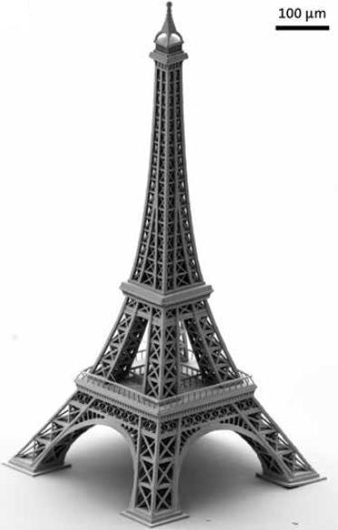
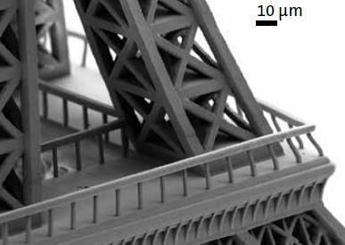
2 Multiphoton lithography Also known as direct laser lithography, direct laser writing or two-photon polymerisation Create arbitrary 3D nano/micro structures Based on NIF fs laser induced multi-photon polymerization Direct fabrication without a mask Materials: polymers, ceramics, metals, hybrid Resolution: ~100 nm Femtosecond laser beam Excited state Photoresist Virtual state Lifetime: ~ sec Substrate Ground state


")


3 Micro-stereolithography vs. Multiphoton lithography Micro stereolithography Multiphoton lithography Essential elements CAD design, 2D layer preparation function, laser scanning & controlling system with monitoring devices Mechanism for polymerisation One-photon absorption (Linear absorption) Multi-photon absorption (Non-linear absorption) Laser type UV laser NIR femtosecond laser Resolution ~ 1 µm ~ 100 nm Strategy for 3D fabrication Polymerisation at the surface layer-by-layer approach Polymerisation at any desired location Built 3D structure recording the beam path


4 Systems Nanoscribe Specifications Galvo mode Piezo mode Lateral feature size 200 nm 200 nm Vertical feature size 1500 nm 1000 nm Writing speed Typ. 10 mm/s Typ. 100 µm/s Range Ø 200 µm 300x300x300 µm 3 Accessible writing area 100x100 mm 2 100x100 mm 2
")
5 Fabrication procedure J Biomed Optics 17 (2012)


")
 173133; 90 (2007)")
 993; Optics")
6 Feature size Resolution: ~ 100 nm Methods for making sub-resolution features o With additional radical quenchers o Using highly sensitive initiator o Repolymerization o Combined with stimulated emission depletion (STED) Nanotechnology 16 (2005) 846; Appl Phys Lett 89 (2006) ; 90 (2007) ; Annu Rev of Biochem 78 (2009) 993; Optics Express 21 (2013) 10831; Nano Letters 13 (2013) 5672
7 Materials Compositions o Photoinitiators o Monomer o Requirements o Transparent in the visible and near infrared regions o Fast curing speed so that only the resin in the focal point is polymerized o Resisting to the solvent used in the later washout process o Suitable mechanical property and thermal stability to main the shape

8 Material capability: polymer Multiphoton induced polymerisation

")
9 Material capability: metal Multiphoton induced photoreduction of metal ions Common metals: Ag and Au HAuCl 4 H 2 O Au nanoparticles Nano Today 5 (2010) 435


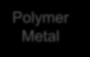

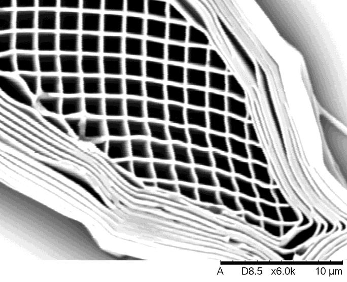
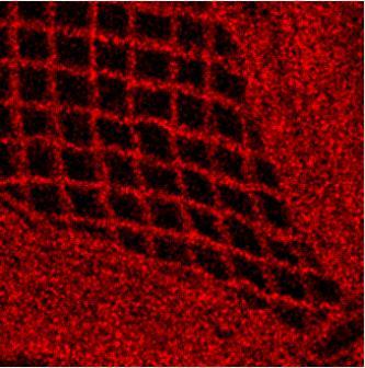
10 Material capability: hybrid Polymer resin + Metallic salts/acids e.g. HAuCl 4 Polymerization Two-photon simultaneously induced Metal reduction Polymer Metal EDX mapping: Au SU8 + Au IP-L + Au

 519; Adv")
11 Material capability: nanomaterials Small amount of nanomaterials mixed with polymer resin to increase the functionality Format: nanoparticles, quantum dots, carbon nanotube Patterns with (c) CdSe and (d) CdSe/ZnS QDs for colour display devices Magnetic turbine with Fe 3 O 4 NPs Optical Materials Express 2(2012) 519; Adv Materials 22 (2010) 3204;
")
12 Material capability: biomaterials Expert Rev Med Devices 9 (2012) 613


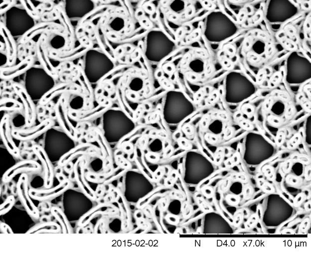
13 Material capability: Casting from polymer Positive photoresist 3D fabricate by multiphoton lithography ITO Deposit Au Remove polymer mould by plasma etching Science 325 (2009) 1513

14 Applications Photonics Micromechanics Cell biology Microfluidics Biomimetics


")


15 Applications: Scaffolds for cell biology J Micromech Microeng 22 (2012) ; Macromol Biosci 12 (2012) 1301; Anal Chem 84 (2012) 8985; Acta Biomaterialia 7 (2011) 967; Biomacromolecules 12 (2011) 851; Biomaterials 31 (2010) 4286; Adv Mater 22 (2010) 868

 22; Laser")
16 Applications: Micro-needles for drug delivery Int J App Cera Tech 4 (2007) 22; Laser Zenturm Hannover


 1993; Lab")
17 Applications: Functional micro-channels Fabricate cell-sized 3D structures in the centre channel (black dashed lines) Lab Chip 10 (2010) 1057; Lab Chip 10 (2010) 1993; Lab Chip 13 (2013) 4800
18 Applications: Magnetic micro-actuator Adv Mater 24 (2012) 811; Opt Lett 34 (2009) 581


19 Applications: Optical-driven micro-rotor Optical trapping and rotation Optical-driven micropump action in a microfluidic channel Phys Rev Lett 109 (2012) ; Optical Express 19 (2011) 8267

20 Applications: Chemical-driven micro-actuator PNAS 105 (2008) 8850; Soft Matter 7 (2011) 10353; Phys Chem Chem Phys 13 (2011) 4835


21 Applications: Biomimetics Gecko-mimicking surface for adhesive Small 8 (2012) 3009


22 Combined with jetting PEGDA film (~20 µm thick) : jetting + UV curing IP-L micro structure on top of PEGDA thin film: two-photon polymerisation Tilted view Top view PEGDA film Bare glass Top view Tilted view
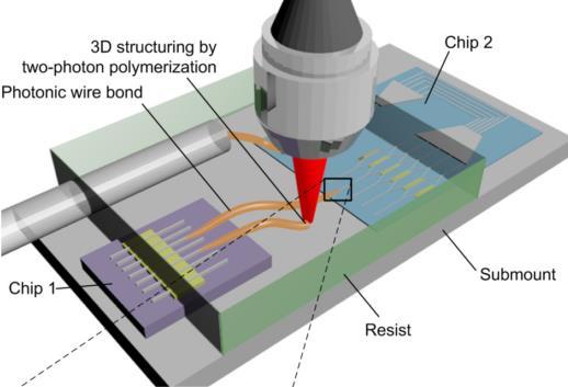
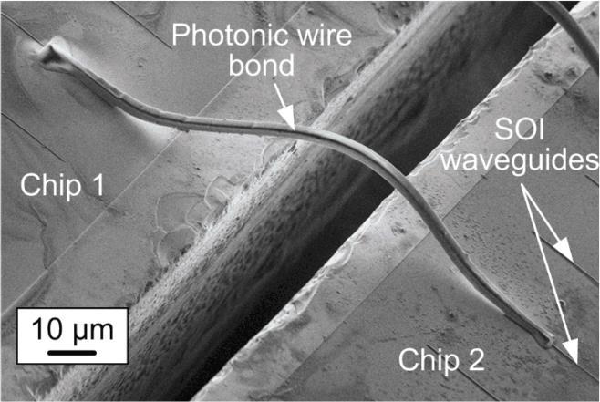

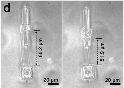
23 Applications: Connection & bonding Appl Opt 52 (2013) 388; Opt Exp 20 (2012) 17667; Appl Phys Lett 100 (2012) ; Nano Today 5 (2010) 435


")
 1256 ; J Opt 12")
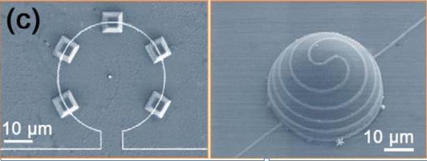
24 Applications: Micro-optics Microlens arrays & their arrays of miniaturized F images Fresnel zone plate Fabricate on the tip of an optical fibre Axicon lens Appl Phys Lett 97 (2010) ; J Opt 12 (2010) ; J Lightwave Tech 28 (2010) 1256 ; J Opt 12 (2010)


 Opt Expr")
 347; Proceeding of")
25 Applications: Waveguides Portable waveguide Portable waveguide Multimode waveguide on PCB Data transfer rate: 7 Gbit/s Handles for optical trapping Plasmonic waveguide A waveguide is placed around a bubble (~ 80 µm) Opt Expr 20 (2012) 2004; Appl Phys A 100 (2010) 347; Proceeding of SPIE (2008);


 11;")
")
26 Applications: Photonic crystals Adv Mater 21 (2009) 4680; Appl Phy Lett 94 (2009) ; Appl Phy A 93 (2008) 11; Optics Express 16 (2008) 15402; Optics Express 16 (2008) 20073;


 115105; Adv Mater 25")
 34; Opt Mater")
27 Applications: Optical metamaterials Manufacturing routes: Two-photon polymerization + metal coating Photopolymerization & photoreduction simultaneously Perfect absorber Phy Rev B 88 (2013) ; Adv Mater 25 (2013) 3994; IEICE Electronics Express 9 (2012) 34; Opt Mater Exp 1 (2011) 1548; Acs Nano 5 (2011) 1947


 1322; PNAS 111 (2014)")
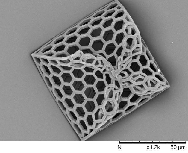
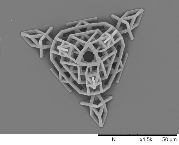
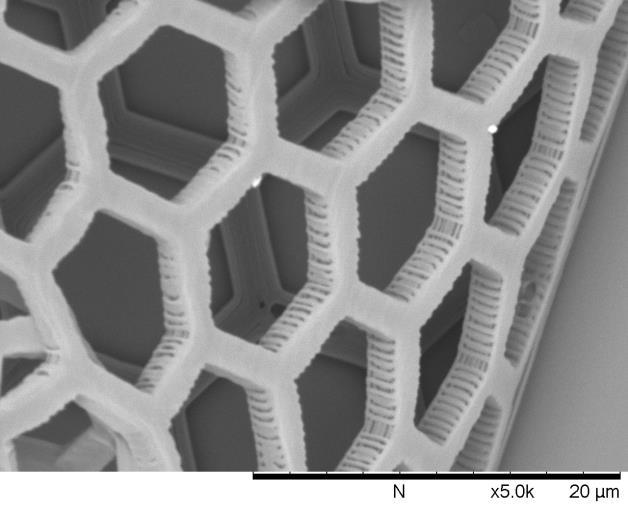
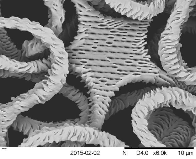
28 Applications: Mechanical metamaterials Artificial structures with mechanical properties defined by structures rather than their composition Nanolattice: strong & lightweight Strength up to 280 MPa! Recoverable Science 345 (2014) 1322; PNAS 111 (2014) 2453 L = 5 µm; a = 650 nm; t = 10 nm
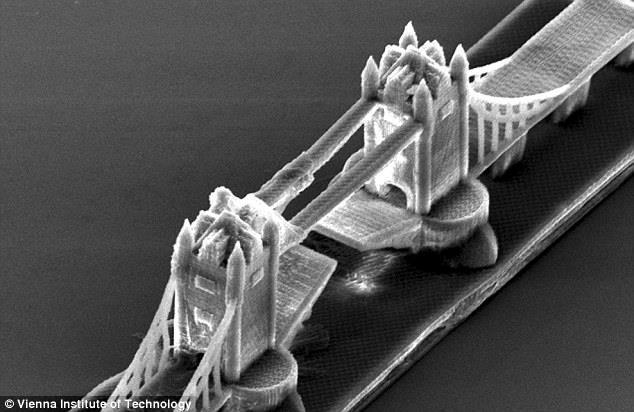
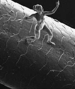
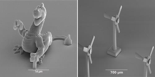
29 Applications: For fun Human hair Nanoscribe, Karlsruhe Institute of Technology, Vienna Institute of Technology, Jonty Hurwitz

30 Send your questions to Dr Qin Hu
Fabrication of micro/nano structures in glass by lasers
 Lehigh University Lehigh Preserve International Workshop on Scientific Challenges for Glass Research Glass Conferences and Workshops Spring 4-1-2007 Fabrication of micro/nano structures in glass by lasers
Fabrication of Micro and Nano Structures in Glass using Ultrafast Lasers
 Fabrication of Micro and Nano Structures in Glass using Ultrafast Lasers Denise M. Krol University of California, Davis IMI Glass Workshop Washington DC April 15-17, 2007 Femtosecond laser modification
Introduction to Micro and Nanotechnologies
 Micro & Nanobioengineering Lab Biomedical Engineering Department McGill University Introduction to Micro and Nanotechnologies David Juncker david.juncker@mcgill.ca www.bmed.mcgill.ca/nanomed McGill, Nov
Soft Fabrication and Polymers
 Introduction to BioMEMS & Medical Microdevices Soft Fabrication and Polymers Companion lecture to the textbook: Fundamentals of BioMEMS and Medical Microdevices, by Prof., http://saliterman.umn.edu/ R012408
EXAMPLES OF INDUSTRIAL APPLICATIONS
 14 EXAMPLES OF INDUSTRIAL APPLICATIONS STEEL FOIL Μ-DRILLING No melting Micron diameter Filters Functional surfaces DIAMOND CUTTING Low carbonization No HAZ Low material loss Diamond sheet cutting Chip
EXAMPLES OF INDUSTRIAL APPLICATIONS
 14 EXAMPLES OF INDUSTRIAL APPLICATIONS STEEL FOIL Μ-DRILLING No melting Micron diameter Filters Functional surfaces DIAMOND CUTTING Low carbonization No HAZ Low material loss Diamond sheet cutting Chip
Femtosecond micromachining in polymers
 Femtosecond micromachining in polymers Prof. Dr Cleber R. Mendonca Daniel S. Corrêa Prakriti Tayalia Dr. Tobias Voss Dr. Tommaso Baldacchini Prof. Dr. Eric Mazur fs-micromachining focus laser beam inside
Nanostructured Plasmonic Interferometers for Ultrasensitive Label-Free Biosensing. Fil Bartoli Lehigh University 4/9/2014
 Nanostructured Plasmonic Interferometers for Ultrasensitive Label-Free Biosensing Fil Bartoli Lehigh University 4/9/2014 P.C. Rossin College of Engineering and Applied Science Department of Electrical
3 Pulsed laser ablation and etching of fused silica
 3 Pulsed laser ablation and etching of fused silica 17 3 Pulsed laser ablation and etching of fused silica Material erosion caused by short laser pulses takes place far from equilibrium and may be based
High-throughput three-dimensional (3D) lithographic microfabrication in biomedical applications
 lithographic microfabrication in biomedical applications") High-throughput three-dimensional (3D) lithographic microfabrication in biomedical applications The MIT Faculty has made this article openly available. Please share how this access benefits you. Your story
High-throughput three-dimensional (3D) lithographic microfabrication in biomedical applications The MIT Faculty has made this article openly available. Please share how this access benefits you. Your story
General Introduction to Microstructure Technology p. 1 What is Microstructure Technology? p. 1 From Microstructure Technology to Microsystems
 General Introduction to Microstructure Technology p. 1 What is Microstructure Technology? p. 1 From Microstructure Technology to Microsystems Technology p. 9 The Parallels to Microelectronics p. 15 The
Laser material processing for a wide range of applications
 Laser material processing for a wide range of applications Paul Hartmann Wien, 29.10.2018 www.joanneum.at/materials 2 Outline 1. Intro: Institute MATERIALS 2. Laser Production Technologies with multi-kw
3D Laser Lithography in Biotechnology and Medical Technology
 3D Laser Lithography in Biotechnology and Medical Technology High-Precision, Piezo-Based Nanopositioning Systems Advance Technology Page 1 of 6 Laser technology makes it possible to create even very complex
Nanoimprinting in Polymers and Applications in Cell Studies. Albert F. YEE Chemical Engineering & Materials Science UC Irvine
 Nanoimprinting in Polymers and Applications in Cell Studies Albert F. YEE Chemical Engineering & Materials Science UC Irvine Presentation outline Motivation Reversal imprinting Soft inkpad imprinting on
Introduction to Nanoscience and Nanotechnology
 Introduction to Nanoscience and Nanotechnology ENS 463 2. Principles of Nano-Lithography by Alexander M. Zaitsev alexander.zaitsev@csi.cuny.edu Tel: 718 982 2812 Office 4N101b 1 Lithographic patterning
Micro and nano structuring of carbon based materials for micro injection moulding and hot embossing
 Micro and nano structuring of carbon based materials for micro injection moulding and hot embossing Victor Usov, Graham Cross, Neal O Hara, Declan Scanlan, Sander Paulen, Chris de Ruijter, Daniel Vlasveld,
NanoSystemsEngineering: NanoNose Final Status, March 2011
 1 NanoSystemsEngineering: NanoNose Final Status, March 2011 The Nanonose project is based on four research projects (VCSELs, 3D nanolithography, coatings and system integration). Below, the major achievements
Contents Preface xiii Introduction Fabrication and manufacturing technology for optical MEMS
 Contents Preface xiii 1 Introduction 1 1.1 Optical MEMS and optofluidics 1 1.2 History 1 1.2.1 Processes and materials 1 1.2.2 Early devices and systems 2 1.3 Progress in optical MEMS and optofluidics
Electricity from the Sun (photovoltaics)
") Electricity from the Sun (photovoltaics) 0.4 TW US Electricity Consumption 100 100 square kilometers of solar cells could produce all the electricity for the US. But they are still too costly. The required
Electricity from the Sun (photovoltaics) 0.4 TW US Electricity Consumption 100 100 square kilometers of solar cells could produce all the electricity for the US. But they are still too costly. The required
Nanotechnology Principles, Applications, Careers, and Education. Copyright 2011 The Pennsylvania State University
 Nanotechnology Principles, Applications, Careers, and Education Copyright 2011 The Pennsylvania State University Outline What are the principles of nanotechnology? What are some applications? What kind
Developing Enhanced Substrates for OLED SSL
 Developing Enhanced Substrates for OLED SSL DOE SSL R&D Manufacturing Workshop San Diego CA 7 May, 2014 Dr. W. Dennis Slafer MicroContinuum, Inc. 57 Smith Place Cambridge, MA 02138 www.microcontinuum.com
Free standing Multilayer Thin Film of Cellulose Nanocrystals
 Free standing Multilayer Thin Film of Cellulose Nanocrystals Chaoyang Jiang Department of Chemistry The University of South Dakota Edmonton, June 25, 2009 Cellulose Nanocrystals Nanotechnology R&D Priority
Plasmonics using Metal Nanoparticles. Tammy K. Lee and Parama Pal ECE 580 Nano-Electro-Opto-Bio
 Plasmonics using Metal Nanoparticles Tammy K. Lee and Parama Pal ECE 580 Nano-Electro-Opto-Bio April 1, 2007 Motivation Why study plasmonics? Miniaturization of optics and photonics to subwavelength scales
Micro- and Nano-Technology... for Optics
 Micro- and Nano-Technology...... for Optics 3.2 Lithography U.D. Zeitner Fraunhofer Institut für Angewandte Optik und Feinmechanik Jena Electron Beam Column electron gun beam on/of control magnetic deflection
Simple UV-based Soft-lithography Process for. Fabrication of Low-Loss Polymer PSQ-L-based. Waveguides
 Simple UV-based Soft-lithography Process for Fabrication of Low-Loss Polymer PSQ-L-based Waveguides Jie Teng 1, 2, 4, Stijn Scheerlinck 4, Geert Morthier 4, Roel Baets 4, Hongbo Zhang 2,3, Xigao Jian 2,3,
UV15: For Fabrication of Polymer Optical Waveguides
 CASE STUDY UV15: For Fabrication of Polymer Optical Waveguides Master Bond Inc. 154 Hobart Street, Hackensack, NJ 07601 USA Phone +1.201.343.8983 Fax +1.201.343.2132 main@masterbond.com CASE STUDY UV15:
Three-Dimensional Laser Writing on the Nanometer Scale
 Three-Dimensional Laser Writing on the Nanometer Scale Piezo Drives are Driving Technology Forward Page 1 of 5 The best possible positioning accuracy is now mandatory in many fields of application. The
High Sensitivity of Phase-based Surface Plasmon Resonance in Nano-cylinder Array
 PIERS ONLINE, VOL. 4, NO. 7, 2008 746 High Sensitivity of Phase-based Surface Plasmon Resonance in Nano-cylinder Array Bing-Hung Chen, Yih-Chau Wang, and Jia-Hung Lin Institute of Electronic Engineering,
Supporting Information. Low Temperature Oxidation-free Selective Laser Sintering of Cu
 Supporting Information Low Temperature Oxidation-free Selective Laser Sintering of Cu Nanoparticle Paste on a Polymer Substrate for the Flexible Touch Panel Applications Jinhyeong Kwon 1,, Hyunmin Cho
Simple fabrication of highly ordered AAO nanotubes
 Journal of Optoelectronic and Biomedical Materials Volume 1, Issue 1, March 2009, p. 79-84 Simple fabrication of highly ordered AAO nanotubes N. Taşaltin a, S. Öztürk a, H. Yüzer b, Z. Z. Öztürk a,b* a
Vertically aligned Ni magnetic nanowires fabricated by diblock-copolymer-directed Al thin film anodization
 Vertically aligned Ni magnetic nanowires fabricated by diblock-copolymer-directed Al thin film anodization Researcher: Kunbae (Kevin) Noh, Graduate Student, MAE Dept. and CMRR Collaborators: Leon Chen,
Compact hybrid plasmonic-si waveguide structures utilizing Albanova E-beam lithography system
 Compact hybrid plasmonic-si waveguide structures utilizing Albanova E-beam lithography system Introduction Xu Sun Laboratory of Photonics and Microwave Engineering, Royal Institute of Technology (KTH),
TEMPERATURE-DEPENDENT REFRACTIVE INDICES OF OPTICAL PLANAR WAVEGUIDES
 TEMPERATURE-DEPENDENT REFRACTIVE INDICES OF OPTICAL PLANAR WAVEGUIDES Aiman Kassir a, Abang Annuar Ehsan b, Noraspalelawati Razali b, Mohd Kamil Abd Rahman a and Sahbudin Shaari b Faculty of Applied Sciences,
Outline. Introduction to the LIGA Microfabrication Process. What is LIGA? The LIGA Process. Dr. Bruce K. Gale Fundamentals of Microfabrication
 Outline Introduction to the LIGA Microfabrication Process Dr. Bruce K. Gale Fundamentals of Microfabrication What is LIGA? The LIGA Process Lithography Techniques Electroforming Mold Fabrication Analyzing
PATTERNING OF OXIDE THIN FILMS BY UV-LASER ABLATION
 Journal of Optoelectronics and Advanced Materials Vol. 7, No. 3, June 2005, p. 1191-1195 Invited lecture PATTERNING OF OXIDE THIN FILMS BY UV-LASER ABLATION J. Ihlemann * Laser-Laboratorium Göttingen e.v.,
Unit title: Nanotechnology
 Unit title: Nanotechnology Unit code: K/601/0311 QCF level: 4 Credit value: 15 Aim This unit examines the role of nanotechnology at the interface of Chemistry, Biology, Physics and Engineering, especially
FABRICATION FOR MICRO PATTERNS OF NICKEL MATRIX DIAMOND COMPOSITES USING THE COMPOSITE ELECTROFORMING AND UV- LITHOGRAPHY
 16 TH INTERNATIONAL CONFERENCE ON COMPOSITE MATERIALS FABRICATION FOR MICRO PATTERNS OF NICKEL MATRIX DIAMOND COMPOSITES USING THE COMPOSITE ELECTROFORMING AND UV- LITHOGRAPHY Tsung-Han Yu, Shenq-Yih Luo,
Light-driven micro-tool equipped with a syringe function
 Supplementary information Light-driven micro-tool equipped with a syringe function Mark Jayson Villangca 1, Darwin Palima 1, Andrew Rafael Bañas 2 and Jesper Glückstad 1 * 1DTU Fotonik, Dept. of Photonics
Laser Micromachining of Bulk Substrates and Thin Films Celine Bansal
 Laser Micromachining of Bulk Substrates and Thin Films Celine Bansal Oxford Lasers Ltd Moorbrook Park Didcot, Oxfordshire, OX11 7HP Tel: +44 (0) 1235 810088 www.oxfordlasers.com Outline Oxford Lasers Importance
Introduction to Lithography
 Introduction to Lithography G. D. Hutcheson, et al., Scientific American, 290, 76 (2004). Moore s Law Intel Co-Founder Gordon E. Moore Cramming More Components Onto Integrated Circuits Author: Gordon E.
Laser micromachining for manufacturing MEMS devices
 Invited Paper Laser micromachining for manufacturing MEMS devices Malcolm Gower Exitech Ltd, Hanborough Park, Long Hanborough, Oxford OX8 8LH, England ABSTRACT Applications of laser micromachining to the
Nano-imprinting Lithography Technology І
 Nano-imprinting Lithography Technology І Agenda Limitation of photolithograph - Remind of photolithography technology - What is diffraction - Diffraction limit Concept of nano-imprinting lithography Basic
Advanced Polymers And Resists For Nanoimprint Lithography
 Q U A L I T Y A S S U R A N C E MICROSYSTEMS & NANOSYSTEMS SPECIAL REPORT Advanced Polymers And Resists For Nanoimprint Lithography Numerous polymer systems specifically designed for nanoimprint lithography
Polymer-based optical interconnects using nano-imprint lithography
 Polymer-based optical interconnects using nano-imprint lithography Arjen Boersma,Sjoukje Wiegersma Bert Jan Offrein, Jeroen Duis, Jos Delis, Markus Ortsiefer, Geert van Steenberge, MikkoKarppinen, Alfons
Mikrosensorer. Microfabrication 1
 Mikrosensorer Microfabrication 1 Literature Introductory MEMS Fabrication and Applications Thomas M. Adams and Richard A. Layton Available as ebook on http://www.lub.lu.se/en/search/lubsearch.html This
Polymer-based Microfabrication
 Polymer-based Microfabrication PDMS SU-8 PMMA Hydrogel 1 Soft Lithography Developed by Whitesides, et. al A set of techniques for microfabrication based on the use of lithography, soft substrate materials
Photonics applications IV. Fabrication of GhG optical fiber Fabrication of ChG planar waveguide Fabrication of ChG PC structure
 Photonics applications IV Fabrication of GhG optical fiber Fabrication of ChG planar waveguide Fabrication of ChG PC structure 1 Why does fabrication issue matter for photonics applications? Geometrical
Surface Acoustic Wave fabrication using nanoimprint. Zachary J. Davis, Senior Consultant,
 Surface Acoustic Wave fabrication using nanoimprint Zachary J. Davis, Senior Consultant, zjd@teknologisk.dk Center for Microtechnology & Surface Analysis Micro and Nano Technology Sensor Technology Top
Fraunhofer ENAS Current results and future approaches in Wafer-level-packaging FRANK ROSCHER
 Fraunhofer ENAS - Current results and future approaches in Wafer-level-packaging FRANK ROSCHER Fraunhofer ENAS Chemnitz System Packaging Page 1 System Packaging Outline: Wafer level packaging for MEMS
Introduction to Micro/Nano Fabrication Techniques. Date: 2015/05/22 Dr. Yi-Chung Tung. Fabrication of Nanomaterials
 Introduction to Micro/Nano Fabrication Techniques Date: 2015/05/22 Dr. Yi-Chung Tung Fabrication of Nanomaterials Top-Down Approach Begin with bulk materials that are reduced into nanoscale materials Ex:
Two-photon polymerization in 3D Printing sets new Standards in Micro and Nanofabrication. Nanoscribe GmbH Alexander Legant
 Two-photon polymerization in 3D Printing sets new Standards in Micro and Nanofabrication Nanoscribe GmbH Alexander Legant legant@nanoscribe.com Northwestern University Evanston, IL 1 Alexander Legant 22-September
LOW TEMPERATURE PHOTONIC SINTERING FOR PRINTED ELECTRONICS. Dr. Saad Ahmed XENON Corporation November 19, 2015
 LOW TEMPERATURE PHOTONIC SINTERING FOR PRINTED ELECTRONICS Dr. Saad Ahmed XENON Corporation November 19, 2015 Topics Introduction to Pulsed Light Photonic sintering for Printed Electronics R&D Tools for
Red luminescence from Si quantum dots embedded in SiO x films grown with controlled stoichiometry
 Red luminescence from Si quantum dots embedded in films grown with controlled stoichiometry Zhitao Kang, Brannon Arnold, Christopher Summers, Brent Wagner Georgia Institute of Technology, Atlanta, GA 30332
High Speed Sintering for 3D printing applications
 High Speed Sintering for 3D printing applications High Speed Sintering for 3D printing applications Neil Hopkinson, Adam Ellis, Adam Strevens, Manolis Papastavrou and Torben Lange, Xaar plc Introduction
Supplementary Materials
 Supplementary Materials Hierarchical Nanolattice Design The hierarchical nanolattices fabricated in this work are designed using a recursive method that combines different unit cells into hierarchical
PHYS 534 (Fall 2008) Process Integration OUTLINE. Examples of PROCESS FLOW SEQUENCES. >Surface-Micromachined Beam
 Process Integration OUTLINE. Examples of PROCESS FLOW SEQUENCES. >Surface-Micromachined Beam") PHYS 534 (Fall 2008) Process Integration Srikar Vengallatore, McGill University 1 OUTLINE Examples of PROCESS FLOW SEQUENCES >Semiconductor diode >Surface-Micromachined Beam Critical Issues in Process
PHYS 534 (Fall 2008) Process Integration Srikar Vengallatore, McGill University 1 OUTLINE Examples of PROCESS FLOW SEQUENCES >Semiconductor diode >Surface-Micromachined Beam Critical Issues in Process
Choi, Jun-Hyuk Korea Institute of Machinery & Materials
 The 11 th US-Korea Nanosymposium Choi, Jun-Hyuk 2014. 09. 29 Korea Institute of Machinery & Materials About KIMM Nano-research Bldg Clean RM Five Research Divisions; 1. Advanced Manufacturing Sys. 2. Extreme
Additive Manufacturing Technology
 Additive Manufacturing Technology ME 012193 Spring I 2018 By Associate Prof. Xiaoyong Tian Cell:13709114235 Email: leoxyt@mail.xjtu.edu.cn Lecture 02 Fundmental AM processes Interactions in AM processes
micromachines ISSN X
 Micromachines 2012, 3, 55-61; doi:10.3390/mi3010055 Article OPEN ACCESS micromachines ISSN 2072-666X www.mdpi.com/journal/micromachines Surface Plasmon Excitation and Localization by Metal-Coated Axicon
Solutions with Light. Energy and environment, Information and communication, Healthcare and medical technology, Safety and mobility.
 Fraunhofer Institute for Applied Optics and Precision Engineering Solutions with Light EXPERTISE in Optical system technology 2 Solutions with Light The Fraunhofer IOF conducts application oriented research
Towards scalable fabrication of high efficiency polymer solar cells
 Towards scalable fabrication of high efficiency polymer solar cells Hui Joon Park 2*, Myung-Gyu Kang 1**, Se Hyun Ahn 3, Moon Kyu Kang 1, and L. Jay Guo 1,2,3 1 Department of Electrical Engineering and
Ostemer 322 Crystal Clear
 Ostemer 322 Crystal Clear Overview Name Description Recommended applications (see ostemers.com for references) Storage Handling Ostemer 322 Crystal Clear A dual cure polymer (UV + heat) with high transparency
average diameter = 3 nm, from PlasmaChem) was mixed in NLCs to produce QDembedded
 was mixed in NLCs to produce QDembedded") Electronic Supplementary Material (ESI) for RSC Advances. This journal is The Royal Society of Chemistry 2014 Supporting information Experimental Section The blended CLC-monomer materials used to fabricate
Electronic Supplementary Material (ESI) for RSC Advances. This journal is The Royal Society of Chemistry 2014 Supporting information Experimental Section The blended CLC-monomer materials used to fabricate
A method for fabricating a micro-structured surface of polyimide with open and closed pores
 A method for fabricating a micro-structured surface of polyimide with open and closed pores Yong-Won Ma a, Jae Yong Oh b, Seokyoung Ahn c, Bo Sung Shin a,d, * a Department of Cogno-Mechatronics Engineering,
Applications of Nano Patterning Process 1. Patterned Media
 Applications of Nano Patterning Process 1. Patterned Media Contents Introduction Part. 1. Nanoimprinting on Glass Substrate for Patterned Media Part. 2. Nanoinjection Molding of Nanopillars for Patterned
Fs- Using Ultrafast Lasers to Add New Functionality to Glass
 An IMI Video Reproduction of Invited Lectures from the 17th University Glass Conference Fs- Using Ultrafast Lasers to Add New Functionality to Glass Denise M. Krol University of California, Davis 17th
Three-dimensional SU-8 structures by reversal UV imprint
 Three-dimensional SU-8 structures by reversal UV imprint W. Hu, a B. Yang, C. Peng, and S. W. Pang b Solid State Electronics Laboratory, Department of Electrical Engineering and Computer Science, The University
Nanoscale Materials Inspires Innovation and Drives Economic Development
 Nanoscale Materials Inspires Innovation and Drives Economic Development 5nm Greg Salamo & Alex Biris InAs Quantum Dots What is Nanoscience? The effort to understand and design structures at the nano size
Impact of Zinc Oxide on the UV Absorbance and Mechanical Properties of UV Cured Films
 Impact of Zinc Oxide on the UV Absorbance and Mechanical Properties of UV Cured Films R. K. SONI, MEENU TEOTIA* Department of Chemistry C.C.S, University, Meerut Ultraviolet radiation [UVR] UVR is divided
Lab-on-a-Chip (LOC) Miniaturization on micro- and nanoscale.
 Miniaturization on micro- and nanoscale.") Lab-on-a-Chip (LOC) Miniaturization on micro- and nanoscale http://nanob2a.cin2.es/publication/articles/integrated-optical-devices-for-lab-on-a-chip-biosensing-applications, downloaded 14.04.16 www.kit.edu
Lab-on-a-Chip (LOC) Miniaturization on micro- and nanoscale http://nanob2a.cin2.es/publication/articles/integrated-optical-devices-for-lab-on-a-chip-biosensing-applications, downloaded 14.04.16 www.kit.edu
Cristaux 3D. Fabriquer de tels objets aux longueur d'ondes optiques???
 Cristaux 3D Fabriquer de tels objets aux longueur d'ondes optiques??? A la main, une sphère l'une après l'autre... 5μm 5μm dissolve latex spheres 4-layer [111] silica diamond lattice 6-layer [001] silica
Chapter 3 Silicon Device Fabrication Technology
 Chapter 3 Silicon Device Fabrication Technology Over 10 15 transistors (or 100,000 for every person in the world) are manufactured every year. VLSI (Very Large Scale Integration) ULSI (Ultra Large Scale
Innovative Roll-to-Roll Equipment & Material Development Suite
 Innovative Roll-to-Roll Equipment & Material Development Suite For Next Generation Technology from Carpe Diem Technologies and the University of Massachusetts Amherst By John Berg, Dimitur Benchev, James
EUV Transmission Lens Design and Manufacturing Method
 1 EUV Transmission Lens Design and Manufacturing Method Kenneth C. Johnson kjinnovation@earthlink.net 7/16/2018 http://vixra.org/abs/1807.0188 Abstract This paper outlines a design for an EUV transmission
Efficient waveguide mode extraction in white organic light emitting diodes using ITO-anodes with integrated MgF 2 -columns
 Efficient waveguide mode extraction in white organic light emitting diodes using ITO-anodes with integrated MgF 2 -columns Tobias Bocksrocker, 1, * Florian Maier-Flaig, 1 Carsten Eschenbaum, 1 and Uli
Verfahrens- und Systemtechnik zum präzisen Hochleistungsabtrag mit UKP-Lasern
 Verfahrens- und Systemtechnik zum präzisen Hochleistungsabtrag mit UKP-Lasern Jens Holtkamp Motivation Ultra short pulsed lasers National Institute of Standards and Technology (NIST) Regional Laser and
Laser treatment of gravure-printed ITO films on PET
 Laser treatment of gravure-printed ITO films on PET Howard V Snelling, Anton A Serkov, Jack Eden, Rob J Farley Physics, School of Mathematical and Physical Sciences, University of Hull, HU6 7RX, UK Presentation
Enhanced Light Trapping in Periodic Aluminum Nanorod Arrays as Cavity Resonator
 Enhanced Light Trapping in Periodic Aluminum Nanorod Arrays as Cavity Resonator Rosure B. Abdulrahman, Arif S. Alagoz, Tansel Karabacak Department of Applied Science, University of Arkansas at Little Rock,
Preface Preface to First Edition
 Contents Foreword Preface Preface to First Edition xiii xv xix CHAPTER 1 MEMS: A Technology from Lilliput 1 The Promise of Technology 1 What Are MEMS or MST? 2 What Is Micromachining? 3 Applications and
EECS130 Integrated Circuit Devices
 EECS130 Integrated Circuit Devices Professor Ali Javey 9/13/2007 Fabrication Technology Lecture 1 Silicon Device Fabrication Technology Over 10 15 transistors (or 100,000 for every person in the world)
Photonic Drying Pulsed Light as a low Temperature Sintering Process
 Photonic Drying Pulsed Light as a low Temperature Sintering Process Lou Panico Xenon Corporation W E S T E R N M I C H I G A N U N I V E R S I T Y PRESENTATION OVERVIEW What is Printed Electronics Materials
Department of Chemistry, University of California, Davis, California 95616, USA 2
 Enhance Solar Water Splitting Performance by Utilizing Near Infrared Radiation with Composite Films of Hematite and Rare Earth Doped Upconversion Materials Ming Zhang, 1 Yongjing Lin, 2 Thomas J. Mullen,
Lecture 6. Through-Wafer Interconnect. Agenda: Through-wafer Interconnect Polymer MEMS. Through-Wafer Interconnect -1. Through-Wafer Interconnect -2
 Agenda: EEL6935 Advanced MEMS (Spring 2005) Instructor: Dr. Huikai Xie Lecture 6 Through-wafer Interconnect EEL6935 Advanced MEMS 2005 H. Xie 1/21/2005 1 Motivations: Wafer-level packaging CMOS 3D Integration
An easily coatable temperature responsive cholesteric liquid. crystal oligomers for making structural colour patterns
 Electronic Supplementary Material (ESI) for Journal of Materials Chemistry C. This journal is The oyal Society of Chemistry 2018 Supporting Information An easily coatable temperature responsive cholesteric
Photoresist Coat, Expose and Develop Laboratory Dr. Lynn Fuller
 ROCHESTER INSTITUTE OF TECHNOLOGY MICROELECTRONIC ENGINEERING Photoresist Coat, Expose and Develop Laboratory Dr. Lynn Fuller Webpage: http://www.rit.edu/lffeee 82 Lomb Memorial Drive Rochester, NY 14623-5604
Macroscopic Arrays of Block Copolymers with Areal Densities of 10 Terbit/inch 2 and Beyond
 Macroscopic Arrays of Block Copolymers with Areal Densities of 10 Terbit/inch 2 and Beyond Soojin Park*, Dong Hyun Lee, Bokyung Kim, Sung Woo Hong Department of Polymer Science and Engineering, University
MICROFLUIDIC STRUCTURES FOR SINGLE CELL ANALYSIS
 MICROFLUIDIC STRUCTURES FOR SINGLE CELL ANALYSIS CAROLINE BECK ADIELS MICRO- AND NANOPROCESSING TECHNOLOGIES, MARCH 2015 What is microfluidics? Fairly young, interdisciplinary research field Evolved from:
Fabrication of Gold Microelectrodes on a Glass Substrate by. Femtosecond-Laser-Assisted Electroless Plating
 JLMN-Journal of Laser Micro/Nanoengineering Vol. 7, No. 3, 2012 Fabrication of Gold Microelectrodes on a Glass Substrate by Femtosecond-Laser-Assisted Electroless Plating Jiangxin Song*1, Yang Liao*1,
Production and analysis of optical gratings and nanostructures created by laser based methods
 Summary of the Ph.D. thesis Production and analysis of optical gratings and nanostructures created by laser based methods Kiss Bálint Supervisor: Dr. Vass Csaba Research fellow Doctoral School in Physics
EUV Transmission Lens Design and Manufacturing Method
 1 EUV Transmission Lens Design and Manufacturing Method Kenneth C. Johnson kjinnovation@earthlink.net 7/9/2018 Abstract This paper outlines a design for an EUV transmission lens comprising blazed, phase-
Micro-Nano Fabrication Research
 Micro-Nano Fabrication Research Technical Education Quality Improvement Programme 22-23 December 2014 Dr. Rakesh G. Mote Assistant Professor Department of Mechanical Engineering IIT Bombay rakesh.mote@iitb.ac.in;
Dielectric II-VI and IV-VI Metal Chalcogenide Thin Films in Hollow Glass Waveguides (HGWs) for Infrared Spectroscopy and Laser Delivery
 for Infrared Spectroscopy and Laser Delivery") Dielectric II-VI and IV-VI Metal Chalcogenide Thin Films in Hollow Glass Waveguides (HGWs) for Infrared Spectroscopy and Laser Delivery Carlos M. Bledt * a, Daniel V. Kopp a, and James A. Harrington a
Dielectric II-VI and IV-VI Metal Chalcogenide Thin Films in Hollow Glass Waveguides (HGWs) for Infrared Spectroscopy and Laser Delivery Carlos M. Bledt * a, Daniel V. Kopp a, and James A. Harrington a
Deep Lithography for Microfabrication
 Deep Lithography for Microfabrication Part 2: UV Deep Lithography (UVDL) Luiz O. S. Ferreira Mechanical Engineering Faculty Campinas State University UNICAMP Campinas SP - BRAZIL lotavio@fem.unicamp.br
A silicon nanocrystals/polymer nanocomposite as down-conversion layer in organic and hybrid solar cells
 Electronic Supplementary Material (ESI) for Nanoscale. This journal is The Royal Society of Chemistry 2015 Supporting Material for A silicon nanocrystals/polymer nanocomposite as down-conversion layer
Illuminating Innovations
 Illuminating Innovations TM Silicone Solutions for LED Packaging Emir Debastiani Application Engineer Dow Corning Brazil Email: emir.debastiani@dowcorning.com Table of Contents Dow Corning Introduction
Lecture 13 Nanophotonics in plasmonics. EECS Winter 2006 Nanophotonics and Nano-scale Fabrication P.C.Ku
 Lecture 13 Nanophotonics in plasmonics EECS 598-002 Winter 2006 Nanophotonics and Nano-scale Fabrication P.C.Ku Schedule for the rest of the semester Introduction to light-matter interaction (1/26): How
Efficiency Enhancement of Bulk-Heterojunction
 Efficiency Enhancement of Bulk-Heterojunction Hybrid Solar Cells Michael Krüger, Yunfei Zhou, Michael Eck Freiburg Materials Research Centre (FMF), University of Freiburg, Germany Institute for Microsystems
Lasers in Advanced Packaging
 Lasers in Advanced Packaging Xiangyang Song, Cristian Porneala, Dana Sercel, Kevin Silvia, Joshua Schoenly, Rouzbeh Sarrafi, Sean Dennigan, Eric DeGenova, Scott Tompkins, Brian Baird, Vijay Kancharla,
Aligned Carbon Nanofibre-Polymer Composite Membranes. CNT Growth and Manipulation. Eleanor Campbell Dept. of Physics, Göteborg University
 Aligned Carbon Nanofibre-Polymer Composite Membranes CNT Growth and Manipulation Eleanor Campbell Dept. of Physics, Göteborg University Plasma CVD Growth Polymer/Nanofibre Composite Low ambient temperature
Nanotechnology: The road for a better future. Prof. Uriel Levy
 Nanotechnology: The road for a better future Prof. Uriel Levy March 2016 The Nano-concept is in broad use but what is really Nano Science? Small is Different! Human Hair 100,000 smaller Molecule Nano size