Tackling the optical interconnection challenge for the Integrated Photonics Revolution
|
|
|
- Samuel Chapman
- 6 years ago
- Views:
Transcription
1 Tackling the optical interconnection challenge for the Integrated Photonics Revolution Dr. Ir. TU Delft, Precision and Microsystems Engineering

![Ants Foot [Digital mirror array, TI] [IBM]](/docs-images/74/69871726/images/2-2.jpg "Same technology basis for creating")

2 Microfabrication and MEMS Si microfabrication the backbone for success of microelectronics Ants Foot [Digital mirror array, TI] [IBM] Same technology basis for creating micromechanical functions: MEMS MicroElectroMechanical Functions Accelerometers, inkjet heads, resonators,


3 Exploit Microfabrication and MEMS for science and industry Precision and sensitivity Small size and integration potential Volume scalability
4 Message of the day Show that microfabrication and MEMS is a promising enabler for breakthrough in the assembly and precision alignment for photonic devices The challenge: integrated photonics, packages and alignment The proposed solution: concept, design and manufacture results

5 Integrated Photonics Philosophy: photonic building blocks Courtesy:


6 Integrated Photonics to design and fabricate a variety of functions Lasers Passive devices Switches and modulators Multi project wafer run to share cost in R&D phase Courtesy:
 to chip Precision level depends on mode field diameter and wavelength In most demanding cases deep sub µm")
7 Alignment challenge Optical interfacing: internal and external, e.g. Optical components within package Fibre (array) to chip Precision level depends on mode field diameter and wavelength In most demanding cases deep sub µm (±100nm)


8 Electronic vs optical assembly/packaging The need: high precision, low(er) cost, higher throughput, higher levels of automation

9 Microfabrication as enabler for photonic alignment


10 Photonics for data communication Photonic packages to enable massive data communication Complex packages: Photonic Integrated Circuit (PIC), micro optics, Integration is a key challenge Technology exists for assembly, however: Labour intensive Expensive

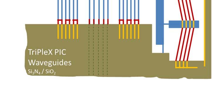
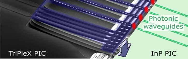
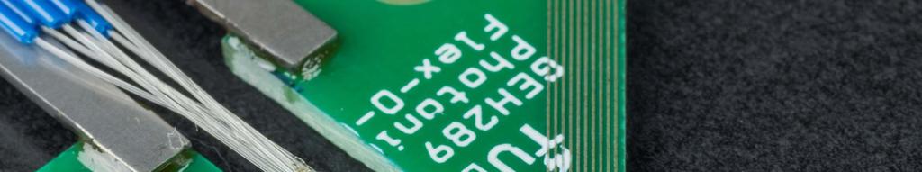
11 New generation: multi chip package InP PIC with TriPleX interposer, coupled to optical fibre array Courtesy:
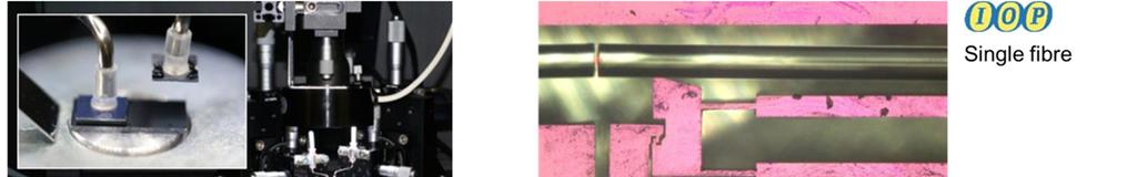
12 Chip to chip alignment Multiple optical ports High precision, waveguide to waveguide (100nm)


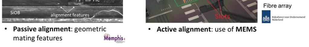
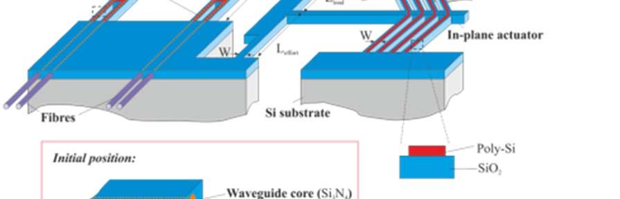
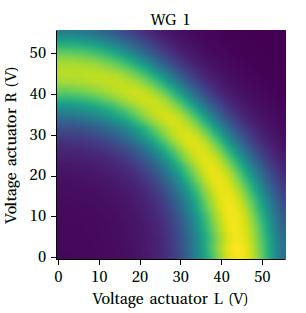
13 On chip MEMS Pre assembly: chips placed and bonded with moderate precision On chip MEMS for fine alignment and locking to final precision, <100nm, waveguide to waveguide TriPleX Shared substrate InP On chip functions: Flexible waveguides Actuators for 3 critical motion directions:,, Locking in final position 19th January 2017 PHASTFlex Project Review, Brussels 13
 motion (Tx) Lever")
14 Design concept InP PIC Waveguides Cross bar Two bimorph actuator sets Short loop actuators Out Of Plane (OOP) motion (Ty, Rz) SiO 2 + Si Suspended SiO 2 Heater / poly Si Conductor TriPleX PIC Waveguides Si 3 N 4 / SiO 2 Flexible waveguide beams Chevron actuator In Plane (IP) motion (Tx) Lever mechanism


15 Design concept


16 SiO 2 photonic MEMS the challenges


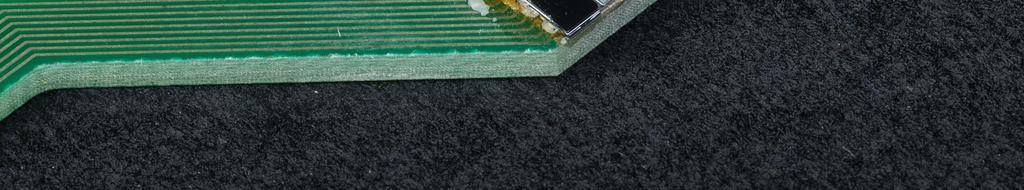
17 Example structure: waveguide beams and bimorphs Post fabrication of TriPleX wafers Fabricated at


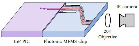
18 MEMS chip packaged for laboratory testing
19


20 Post release curvature and bimorph actuation Temperature ranges during fabrication CTE s of materials

21 In plane motion Chevron actuator: SiO 2 beams with poly Si on top Low CTE of SiO 2 limits motion range motion amplification by lever mechanism Fabricated at

22 Out of plane / bimorph actuators Short loop bimorph actuators Left/Right performance not equal due to mechanical cross sensitivity, connection with in plane actuation structure L R

23 In plane / chevron actuation Designed motion amplification: ~3.3, measured ~3.4 In plane motion ~125mW, approaching required level

24 Optical coupling


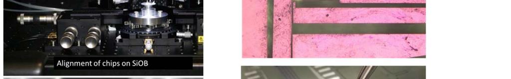
25 Pre assembly Chip placement, bonding, and electrical interconnection (DC, RF) Moderate precision : few µm Is in reach of advanced industrial die bonders LTCC InP TriPleX
26 Conclusions Microfabrication and MEMS offer potential for new assembly concepts for the photonic domain Various scenarios: Passive alignment: microfabrication offers precision Active alignment: actuator functions for fine alignment in two step assembly process Potential for breakthrough solution: volume compatible assembly of advanced photonic packages
27 Acknowledgement TU Delft co workers Tjitte Jelte Peters, Kai Wu, Alexandre Beck Funding STW GTIP grant 11355, Flex O Guides EU FP7 grant , PHASTFlex, Collaborators from partners, user committee members
28 Further reading Wu, K., Tichem, M. In plane positioning of flexible silicon dioxide photonic waveguides, International Conference on Manipulation, Automation and Robotics at Small Scales (MARSS 2017), July 17 21, 2017, Montréal, Canada Peters, T. J. and M. Tichem, Electrothermal Actuators for SiO 2 Photonic MEMS, Micromachines, 2016, 7, 200; doi: /mi Peters. T. J., Tichem, M., On chip positionable photonic waveguides for chip to chip optical interconnects, SPIE Photonics Europe, April 2016, Brussels Wörhoff, K., et al, Photonic hybrid assembly through flexible waveguides, SPIE Photonics Europe, April 2016, Brussels Peters, T. J., and Tichem, M., Mechanically flexible waveguide arrays for optical chip to chip coupling, SPIE Photonics West/OPTO, February 2016, San Fransisco, USA Peters, T. J. and M. Tichem, Fabrication and characterization of suspended beam structures for SiO 2 photonic MEMS. Journal of Micromechanics and Microengineering, (10): p Wu, K., Peters, T. J., Tichem, M. et al, Bimorph actuators in thick SiO 2 for photonic alignment, SPIE Photonics West/OPTO, February 2016, San Fransisco, USA Gurp, J.F.C. van, et al., Passive Photonic Alignment With Submicrometer Repeatability and Accuracy. Components, Packaging and Manufacturing Technology, IEEE Transactions on, (11): p Henneken, V.A., M. Tichem, and P. Sarro, In package MEMS based thermal actuators for micro assembly. Journal of Micromechanics and Microengineering, (6): p. S107.

29 Thank you
On-chip MEMS for automated chip-to-chip assembly
 On-chip MEMS for automated chip-to-chip assembly Dr. Ir. Marcel Tichem, Ir. Tjitte-Jelte Peters, Kai Wu MSc TU Delft, Precision and Microsystems Engineering Photonics Event, Koningshof, Veldhoven, 2 June
Preface Preface to First Edition
 Contents Foreword Preface Preface to First Edition xiii xv xix CHAPTER 1 MEMS: A Technology from Lilliput 1 The Promise of Technology 1 What Are MEMS or MST? 2 What Is Micromachining? 3 Applications and
Compact hybrid plasmonic-si waveguide structures utilizing Albanova E-beam lithography system
 Compact hybrid plasmonic-si waveguide structures utilizing Albanova E-beam lithography system Introduction Xu Sun Laboratory of Photonics and Microwave Engineering, Royal Institute of Technology (KTH),
Lecture 5. SOI Micromachining. SOI MUMPs. SOI Micromachining. Silicon-on-Insulator Microstructures. Agenda:
 EEL6935 Advanced MEMS (Spring 2005) Instructor: Dr. Huikai Xie SOI Micromachining Agenda: SOI Micromachining SOI MUMPs Multi-level structures Lecture 5 Silicon-on-Insulator Microstructures Single-crystal
Fabrication Technology, Part II
 EEL5225: Principles of MEMS Transducers (Fall 2003) Fabrication Technology, Part II Agenda: Process Examples TI Micromirror fabrication process SCREAM CMOS-MEMS processes Wafer Bonding LIGA Reading: Senturia,
Micro/nanophotonics at VTT
 Micro/nanophotonics at VTT Timo Aalto (timo.aalto@vtt.fi) VTT Technical Research Centre of Finland Micro and nanotechnology seminar, St Petersburg, 16 th Nov 2010 2 Outline Overview of micro and nanophotonics
Micro-Electro-Mechanical Systems (MEMS) Fabrication. Special Process Modules for MEMS. Principle of Sensing and Actuation
 Fabrication. Special Process Modules for MEMS. Principle of Sensing and Actuation") Micro-Electro-Mechanical Systems (MEMS) Fabrication Fabrication Considerations Stress-Strain, Thin-film Stress, Stiction Special Process Modules for MEMS Bonding, Cavity Sealing, Deep RIE, Spatial forming
Micro-Electro-Mechanical Systems (MEMS) Fabrication Fabrication Considerations Stress-Strain, Thin-film Stress, Stiction Special Process Modules for MEMS Bonding, Cavity Sealing, Deep RIE, Spatial forming
Gaetano L Episcopo. Introduction to MEMS
 Gaetano L Episcopo Introduction to MEMS What are MEMS? Micro Electro Mechanichal Systems MEMS are integrated devices, or systems of devices, with microscopic parts, such as: Mechanical Parts Electrical
Micro-Electro-Mechanical Systems (MEMS) Fabrication. Special Process Modules for MEMS. Principle of Sensing and Actuation
 Fabrication. Special Process Modules for MEMS. Principle of Sensing and Actuation") Micro-Electro-Mechanical Systems (MEMS) Fabrication Fabrication Considerations Stress-Strain, Thin-film Stress, Stiction Special Process Modules for MEMS Bonding, Cavity Sealing, Deep RIE, Spatial forming
Micro-Electro-Mechanical Systems (MEMS) Fabrication Fabrication Considerations Stress-Strain, Thin-film Stress, Stiction Special Process Modules for MEMS Bonding, Cavity Sealing, Deep RIE, Spatial forming
Chip and system-level integration technologies for silicon photonics
 Chip and system-level integration technologies for silicon photonics Bert Jan Offrein 5th International Symposium for Optical Interconnect in Data Centres Outline The need for integration at component
Proceedings Post Fabrication Processing of Foundry MEMS Structures Exhibiting Large, Out-of-Plane Deflections
 Proceedings Post Fabrication Processing of Foundry MEMS Structures Exhibiting Large, Out-of-Plane Deflections LaVern Starman 1, *, John Walton 1, Harris Hall 1 and Robert Lake 2 1 Sensors Directorate,
5.8 Diaphragm Uniaxial Optical Accelerometer
 5.8 Diaphragm Uniaxial Optical Accelerometer Optical accelerometers are based on the BESOI (Bond and Etch back Silicon On Insulator) wafers, supplied by Shin-Etsu with (100) orientation, 4 diameter and
Dr. Lynn Fuller Webpage:
 ROCHESTER INSTITUTE OF TECHNOLOGY MICROELECTRONIC ENGINEERING Microelectromechanical Systems (MEMs) Process Integration Dr. Lynn Fuller Webpage: http://people.rit.edu/lffeee 82 Lomb Memorial Drive Rochester,
EV Group 300mm Wafer Bonding Technology July 16, 2008
 EV Group 300mm Wafer Bonding Technology July 16, 2008 EV Group in a Nutshell st Our philosophy Our mission in serving next generation application in semiconductor technology Equipment supplier for the
NANOTUBE MICRO-OPTO-MECHANICAL SYSTEMS
 NANOTUBE MICRO-OPTO-MECHANICAL SYSTEMS B. Panchapakesan Delaware MEMS and Nanotech Laboratory, University of Delaware, Newark, DE 19716, USA (Tel: 001-302-831-4062; Email: baloo@ece.udel.edu) INTRODUCTION
Planarization of a CMOS die for an integrated metal MEMS
 Planarization of a CMOS die for an integrated metal MEMS Hocheol Lee*, Michele H. Miller +, Thomas G. Bifano Boston University ABSTRACT This paper describes a planarization procedure to achieve a flat
Hybrid III-V/Si DFB laser integration on a 200 mm fully CMOS-compatible silicon photonics platform
 Hybrid III-V/Si DFB laser integration on a 200 mm fully CMOS-compatible silicon photonics platform B. Szelag 1, K. Hassan 1, L. Adelmini 1, E. Ghegin 1,2, Ph. Rodriguez 1, S. Bensalem 1, F. Nemouchi 1,
Assembly of Mechanically Compliant Interfaces between Optical Fibers and Nanophotonic Chips
 Assembly of Mechanically Compliant Interfaces between Optical Fibers and Nanophotonic Chips T. Barwicz, Y. Taira, H. Numata, N. Boyer, S. Harel, S. Kamlapurkar, S. Takenobu, S. Laflamme, S. Engelmann,
Poly-SiGe MEMS actuators for adaptive optics
 Poly-SiGe MEMS actuators for adaptive optics Blake C.-Y. Lin a,b, Tsu-Jae King a, and Richard S. Muller a,b a Department of Electrical Engineering and Computer Sciences, b Berkeley Sensor and Actuator
Change in stoichiometry
 Measurement of Gas Sensor Performance Gas sensing materials: 1. Sputtered ZnO film (150 nm (Massachusetts Institute of Technology) 2. Sputtered SnO 2 film (60 nm) (Fraunhofer Institute of Physical Measurement
Automating Hybrid Circuit Assembly
 Automating Hybrid Circuit Assembly Die Attach The demand for hybrid circuits has remained strong as emerging and existing applications continue to rely on this proven technology. Developers of applications
General Introduction to Microstructure Technology p. 1 What is Microstructure Technology? p. 1 From Microstructure Technology to Microsystems
 General Introduction to Microstructure Technology p. 1 What is Microstructure Technology? p. 1 From Microstructure Technology to Microsystems Technology p. 9 The Parallels to Microelectronics p. 15 The
TGV and Integrated Electronics
 TGV and Integrated Electronics Shin Takahashi ASAHI GLASS CO., LTD. 1 Ambient Intelligence Green Energy/Environment Smart Factory Smart Mobility Smart Mobile Devices Bio/Medical Security/Biometrics 2 Glass
First Electrically Pumped Hybrid Silicon Laser
 First Electrically Pumped Hybrid Silicon Laser UCSB Engineering Insights Oct 18 th 2006 Mario Paniccia Intel Corporation 1 Sept 18 th 2006 What We are Announcing Research Breakthrough: 1st Electrically
Electrical and Fluidic Microbumps and Interconnects for 3D-IC and Silicon Interposer
 Electrical and Fluidic Microbumps and Interconnects for 3D-IC and Silicon Interposer Li Zheng, Student Member, IEEE, and Muhannad S. Bakir, Senior Member, IEEE Georgia Institute of Technology Atlanta,
Polymer-based optical interconnects using nano-imprint lithography
 Polymer-based optical interconnects using nano-imprint lithography Arjen Boersma,Sjoukje Wiegersma Bert Jan Offrein, Jeroen Duis, Jos Delis, Markus Ortsiefer, Geert van Steenberge, MikkoKarppinen, Alfons
Project EFFORTLESS. Epitaxy Factory of the Future for Transformational Leverage of Europe s Compound Semiconductor EcoSystem
 Project EFFORTLESS Epitaxy Factory of the Future for Transformational Leverage of Europe s Compound Semiconductor EcoSystem Domain: Process Technologies supplying Smart Health, Energy, Manufacturing and
Activities in Plasma Process Technology at SENTECH Instruments GmbH, Berlin. Dr. Frank Schmidt
 Activities in Plasma Process Technology at SENTECH Instruments GmbH, Berlin Dr. Frank Schmidt The Company Company Private company, founded 1990 80 employees ISO 9001 Location Science & Technology Park,
MEMS Packaging Techniques for Silicon Optical Benches
 MEMS Packaging Techniques for Silicon Optical Benches Hayden Taylor David Moore, Mohamed Boutchich, Billy Boyle, Johnny He, Graham McShane, Richard Breen, Rob Wylie CAMBRIDGE UNIVERSITY ENGINEERING DEPARTMENT
MRSI-175Ag Epoxy Dispenser
 MRSI-175Ag Epoxy Dispenser Applications: Microwave & RF Modules MEMS Semiconductor Packaging Multi-Chip Modules Hybrid Circuits Optical Modules Overview The MRSI-175Ag Conductive Epoxy Dispenser handles
Research Projects in Microelectromechanical Systems (MEMS) and Microfluidics
 and Microfluidics") Research Projects in Microelectromechanical Systems (MEMS) and Microfluidics Luc G. Fréchette, Ph.D. Associate Professor Canada Research Chair in Microfluidics and Power MEMS Department of Mechanical Engineering
Research Projects in Microelectromechanical Systems (MEMS) and Microfluidics Luc G. Fréchette, Ph.D. Associate Professor Canada Research Chair in Microfluidics and Power MEMS Department of Mechanical Engineering
Microelectronics. Integrated circuits. Introduction to the IC technology M.Rencz 11 September, Expected decrease in line width
 Microelectronics Introduction to the IC technology M.Rencz 11 September, 2002 9/16/02 1/37 Integrated circuits Development is controlled by the roadmaps. Self-fulfilling predictions for the tendencies
High Throughput Laser Processing of Guide Plates for Vertical Probe Cards Rouzbeh Sarrafi, Dana Sercel, Sean Dennigan, Joshua Stearns, Marco Mendes
 High Throughput Laser Processing of Guide Plates for Vertical Probe Cards Rouzbeh Sarrafi, Dana Sercel, Sean Dennigan, Joshua Stearns, Marco Mendes IPG Photonics - Microsystems Division Outline Introduction
PROJECT PERIODIC REPORT
 PROJECT PERIODIC REPORT Grant Agreement number: 619456 Project acronym: SITOGA Project title: Silicon CMOS compatible transition metal oxide technology for boosting highly integrated photonic devices with
Die Bonder. Flip Chip Bonder Die Sorter
 Die Bonder Flip Chip Bonder Die Sorter T-6000-L/G Precision Die Attach Equipment with the most level of flexibility and customization T-6000-L T-8000-G T-6000-L/G Flexible High Precision Automatic Die
Laser Micromachining - Market Focus. Dr. Andrew Kearsley
 Laser Micromachining - Market Focus Dr. Andrew Kearsley Oxford Lasers Ltd. Moorbrook Park, Didcot OX11 7HP andrew.kearsley@oxfordlasers.com 5th CIR HVM-UK: South East Conference Harwell, 17 November 2005
Automated High-Throughput Assembly for Photonic Packaging
 Automated High-Throughput Assembly for Photonic Packaging IBM Assembly and Test - Bromont IBM Research - Watson / TRL P. Fortier N. Boyer A. Janta-Polczynski E. Cyr R. Langlois Y. Yoshi H. Numata T. Barwicz
Surface Micromachining
 Surface Micromachining Outline Introduction Material often used in surface micromachining Material selection criteria in surface micromachining Case study: Fabrication of electrostatic motor Major issues
ADOPT Winter School Merging silicon photonics and plasmonics
 ADOPT Winter School 2014 Merging silicon photonics and plasmonics Prof. Min Qiu Optics and Photonics, Royal Institute of Technology, Sweden and Optical Engineering, Zhejiang University, China Contents
Building the 21 st Century Integrated Silicon Photonics Ecosystem
 Building the 21 st Century Integrated Silicon Photonics Ecosystem Integrated Photonics is about data and sensing VISION Establish technology, business, and education framework for industry, government,
Design and fabrication of MEMS devices using the integration of MUMPs, trench-refilled molding, DRIE and bulk silicon etching processes
 TB, KR, JMM/184987, 3/12/2004 INSTITUTE OF PHYSICS PUBLISHING JOURNAL OF MICROMECHANICS AND MICROENGINEERING J. Micromech. Microeng. 15 (2005) 1 8 doi:10.1088/0960-1317/15/0/000 Design and fabrication
Challenges and Future Directions of Laser Fuse Processing in Memory Repair
 Challenges and Future Directions of Laser Fuse Processing in Memory Repair Bo Gu, * T. Coughlin, B. Maxwell, J. Griffiths, J. Lee, J. Cordingley, S. Johnson, E. Karagiannis, J. Ehrmann GSI Lumonics, Inc.
LASER MICROFABRICATION OF MULTIFUNCTIONAL DEVICES
 LASER MICROFABRICATION OF MULTIFUNCTIONAL DEVICES Andy Goater, Gary Owen, Julian Burt & Nadeem Rizvi UK Laser Micromachining Centre Laser Microprocessing of Challenging Materials and Architectures AILU
Within-Tier Cooling and Thermal Isolation Technologies for Heterogeneous 3D ICs
 1 Within-Tier Cooling and Thermal Isolation Technologies for Heterogeneous 3D ICs Yue Zhang, Hanju Oh, and Muhannad S. Bakir School of Electrical & Computer Engineering, Georgia Institute of Technology,
Silicon Wafer Processing PAKAGING AND TEST
 Silicon Wafer Processing PAKAGING AND TEST Parametrical test using test structures regularly distributed in the wafer Wafer die test marking defective dies dies separation die fixing (not marked as defective)
MEMS II: January 23. Lab 1: Pop-up mirror - PolyMUMPS - Thermal actuators - Mirror CoventorWare
 MEMS II: January 23 Lab 1: Pop-up mirror - PolyMUMPS - Thermal actuators - Mirror CoventorWare Microelectromechanical Systems (MEMS) Multi-User MEMS Processes (MUMPS) Example Design Anchor hole 2.0 0.5
Evolution of MEMS Technology
 Evolution of MEMS Technology 1 Raksha Sahadev Hukkeri, 2 Shreya Madapurmath, 3 Shreelekha Navale 1,2,3 UG Student, Department of ECE, SDMCET Dharwad Abstract Micro-Electro-Mechanical Systems (MEMS) is
Surface micromachining and Process flow part 1
 Surface micromachining and Process flow part 1 Identify the basic steps of a generic surface micromachining process Identify the critical requirements needed to create a MEMS using surface micromachining
Micro-Electro-Mechanical Systems (MEMS) Fabrication. Special Process Modules for MEMS. Principle of Sensing and Actuation
 Fabrication. Special Process Modules for MEMS. Principle of Sensing and Actuation") Micro-Electro-Mechanical Systems (MEMS) Fabrication Fabrication Considerations Stress-Strain, Thin-film Stress, Stiction Special Process Modules for MEMS Bonding, Cavity Sealing, Deep RIE, Spatial forming
Micro-Electro-Mechanical Systems (MEMS) Fabrication Fabrication Considerations Stress-Strain, Thin-film Stress, Stiction Special Process Modules for MEMS Bonding, Cavity Sealing, Deep RIE, Spatial forming
Welcome MNT Conference 1 Albuquerque, NM - May 2010
 Welcome MNT Conference 1 Albuquerque, NM - May 2010 Introduction to Design Outline What is MEMs Design General Considerations Application Packaging Process Flow What s available Sandia SUMMiT Overview
IMECE A DUAL-EDM REVERSE DAMASCENE PROCESS FOR RF SWITCHES AND OTHER BULK METAL DEVICES
 Proceedings of IMECE 2005 2005 ASME International Mechanical Engineering Congress and Exposition Orlando, Florida, USA, November 5-11, 2005 IMECE2005-8091 A DUAL-EDM REVERSE DAMASCENE PROCESS FOR RF SWITCHES
Lecture 7 CMOS MEMS. CMOS MEMS Processes. CMOS MEMS Processes. Why CMOS-MEMS? Agenda: CMOS MEMS: Fabrication. MEMS structures can be made
 EEL6935 Advanced MEMS (Spring 2005) Instructor: Dr. Huikai Xie CMOS MEMS Agenda: Lecture 7 CMOS MEMS: Fabrication Pre-CMOS Intra-CMOS Post-CMOS Deposition Etching Why CMOS-MEMS? Smart on-chip CMOS circuitry
PHYS 534 (Fall 2008) Process Integration OUTLINE. Examples of PROCESS FLOW SEQUENCES. >Surface-Micromachined Beam
 Process Integration OUTLINE. Examples of PROCESS FLOW SEQUENCES. >Surface-Micromachined Beam") PHYS 534 (Fall 2008) Process Integration Srikar Vengallatore, McGill University 1 OUTLINE Examples of PROCESS FLOW SEQUENCES >Semiconductor diode >Surface-Micromachined Beam Critical Issues in Process
PHYS 534 (Fall 2008) Process Integration Srikar Vengallatore, McGill University 1 OUTLINE Examples of PROCESS FLOW SEQUENCES >Semiconductor diode >Surface-Micromachined Beam Critical Issues in Process
5. Packaging Technologies Trends
 5. Packaging Technologies Trends Electronic products and microsystems continue to find new applications in personal, healthcare, home, automotive, environmental and security systems. Advancements in packaging
MEMS Devices. Fraunhofer Institute for Silicon Technology ISIT. Itzehoe, Germa. any
 Examples of CMP Processess for the Manufacturing of MEMS Devices Gerfried Zwicke er Fraunhofer Institute for Silicon Technology ISIT Itzehoe, Germa any gerfried.zwicker@isit.fraunhofer.de Contents MEMS
IC-Compatible Technologies for Optical MEMS
 < * IC-Compatible Technologies for Optical MEMS Thomas W. Krygowski, Jef& J. Sniegowsk~ Intelligent Mikromachine Department, Sandia National Laboratories, Albuquerque, New Mexico Optical MicroElectroMechanical
FABRICATION OF SWTICHES ON POLYMER-BASED BY HOT EMBOSSING. Chao-Heng Chien, Hui-Min Yu,
 Stresa, Italy, 26-28 April 2006 FABRICATION OF SWTICHES ON POLYMER-BASED BY HOT EMBOSSING, Mechanical Engineering Department, Tatung University 40 Chung Shan N. Rd. Sec. 3 Taipei, Taiwan ABSTRACT In MEMS
IMM Bologna. S3T Workshop, Porto, 6 th -9 th Apr. 2010
 MICRO ELECTRO MECHANICAL SYSTEMS FOR CRACK MONITORINGINAGEING IN INFRASTRUCTURES A. Roncaglia 1, M. Ferri 1, F. Mancarella 1, J. Yan 2, A. A. Seshia 2, K. Soga 2, J. Zalesky 3 1 CNR, Institute of Microelectronics
Smarter sensing solutions
 Easy access to microsystems production through contract manufacturing services Espoo, Finland June 14th 2011 Smarter sensing solutions Colibrys Foundry presentation: Sean Neylon Business Model The Colibrys
THE FOURTEENTH MICROOPTICS CONFERENCE
 THE FOURTEENTH MICROOPTICS CONFERENCE TECHNICAL DIGEST Organized by Vrije Universiteit Brussel Department of Applied Physics and Photonics September 25 (Thu.) September 27 (Sat.), 2008 Diamant Conference
Integrated photonic devices for sensing and optical communication in the near- and mid- IR
 Integrated photonic devices for sensing and optical communication in the near- and mid- IR Dr. Senthil M Ganapathy (smg@orc.soton.ac.uk) Prof. James S Wilkinson (jsw@orc.soton.ac.uk) Motivation: Integrated
Sensors and Actuators Designed and Fabricated in a. Micro-Electro-Mechanical-Systems (MEMS) Course. Using Standard MEMS Processes
 Course. Using Standard MEMS Processes") Sensors and Actuators Designed and Fabricated in a Micro-Electro-Mechanical-Systems (MEMS) Course Using Standard MEMS Processes M.G. Guvench University of Southern Maine guvench@maine.edu Abstract Use
Sensors and Actuators Designed and Fabricated in a Micro-Electro-Mechanical-Systems (MEMS) Course Using Standard MEMS Processes M.G. Guvench University of Southern Maine guvench@maine.edu Abstract Use
Silver Diffusion Bonding and Layer Transfer of Lithium Niobate to Silicon
 Chapter 5 Silver Diffusion Bonding and Layer Transfer of Lithium Niobate to Silicon 5.1 Introduction In this chapter, we discuss a method of metallic bonding between two deposited silver layers. A diffusion
PARASITIC EFFECTS REDUCTION FOR WAFER-LEVEL PACKAGING OF RF-MEMS
 Stresa, Italy, 26-28 April 2006 J. Iannacci 1,2, J. Tian 1, S.M. Sinaga 1, R. Gaddi 2, A. Gnudi 2, and M. Bartek 1 1) HiTeC-DIMES, Delft University of Technology, Mekelweg 4, 2628 CD Delft, the Netherlands
Vertical plasmonic nanowires for 3D nanoparticle trapping
 Vertical plasmonic nanowires for 3D nanoparticle trapping Jingzhi Wu, Xiaosong Gan * Centre for Micro-Photonics, Faculty of Engineering and Industrial Sciences, Swinburne University of Technology, PO Box
Micro and Smart Systems
 Micro and Smart Systems 1. G.K. Ananthasuresh, Mechanical Engineering,IISc IIScsuresh@mecheng.iisc.ernet.in 2. K.J. Vinoy, Electrical Communications Engineering, IISc, kjvinoy@ece.iisc.ernet.in 3. S. Gopalakrishnan,
Important note To cite this publication, please use the final published version (if applicable). Please check the document version above.
. Please check the document version above.") Delft University of Technology Intravascular Ultrasound at the Tip of a Guidewire Concept and First Assembly Steps Stoute, Ronald; Louwerse, Marcus; Henneken, VA; Dekker, Ronald DOI 10.1016/j.proeng.2016.11.461
Delft University of Technology Intravascular Ultrasound at the Tip of a Guidewire Concept and First Assembly Steps Stoute, Ronald; Louwerse, Marcus; Henneken, VA; Dekker, Ronald DOI 10.1016/j.proeng.2016.11.461
Fraunhofer ENAS Current results and future approaches in Wafer-level-packaging FRANK ROSCHER
 Fraunhofer ENAS - Current results and future approaches in Wafer-level-packaging FRANK ROSCHER Fraunhofer ENAS Chemnitz System Packaging Page 1 System Packaging Outline: Wafer level packaging for MEMS
Quality in Electronic Production has a Name: Viscom. System Overview
 Quality in Electronic Production has a Name: Viscom System Overview Successful along the whole line with Viscom Circuit board manufacturing Paste print Finish S3070 AFI-Scan S3054QS Paste print Thick film
Chapter 4 Fabrication Process of Silicon Carrier and. Gold-Gold Thermocompression Bonding
 Chapter 4 Fabrication Process of Silicon Carrier and Gold-Gold Thermocompression Bonding 4.1 Introduction As mentioned in chapter 2, the MEMs carrier is designed to integrate the micro-machined inductor
FABRICATION PROCESSES FOR MAGNETIC MICROACTUATORS WITH POLYSILICON FLEXURES. Jack W. Judy and Richard S. Muller
 FABRICATION PROCESSES FOR MAGNETIC MICROACTUATORS WITH POLYSILICON FLEXURES Jack W. Judy and Richard S. Muller Berkeley Sensor & Actuator Center (BSAC) Department of EECS, University of California, Berkeley,
EE C245 ME C218 Introduction to MEMS Design Fall 2011
 Lecture Outline EE C245 ME C218 Introduction to MEMS Design Fall 2011 Prof. Clark T.-C. Nguyen Dept. of Electrical Engineering & Computer Sciences University of California at Berkeley Berkeley, CA 94720
Challenges of Fan-Out WLP and Solution Alternatives John Almiranez
 Challenges of Fan-Out WLP and Solution Alternatives John Almiranez Advanced Packaging Business Development Asia Introduction to Fan-Out WLP Introduction World of mobile gadgetry continues to rapidly evolve
Chapter 3 Silicon Device Fabrication Technology
 Chapter 3 Silicon Device Fabrication Technology Over 10 15 transistors (or 100,000 for every person in the world) are manufactured every year. VLSI (Very Large Scale Integration) ULSI (Ultra Large Scale
Development and Characterization of 300mm Large Panel ewlb (embedded Wafer Level BGA)
") Development and Characterization of 300mm Large Panel ewlb (embedded Wafer Level BGA) Seung Wook Yoon, Yaojian Lin and Pandi C. Marimuthu STATS ChipPAC Ltd. 5 Yishun Street 23, Singapore 768442 E-mail
Development and Characterization of 300mm Large Panel ewlb (embedded Wafer Level BGA) Seung Wook Yoon, Yaojian Lin and Pandi C. Marimuthu STATS ChipPAC Ltd. 5 Yishun Street 23, Singapore 768442 E-mail
Fraunhofer IZM. All Silicon System Integration Dresden Scope. M. Juergen Wolf
 Fraunhofer IZM All Silicon System Integration Dresden Scope M. Juergen Wolf Fraunhofer IZM All Silicon System Integration - ASSID Dresden, Berlin, Germany Fraunhofer IZM Focus of Activities Materials,
MEMS and Nanotechnology Research at TST
 MEMS and Nanotechnology Research at TST Remco Wiegerink Theo Lammerink Marcel Dijkstra Jeroen Haneveld MESA+ Institute for Nanotechnology University of Twente P.O. Box 217, 7500 AE Enschede The Netherlands
Trench Structure Improvement of Thermo-Optic Waveguides
 International Journal of Applied Science and Engineering 2007. 5, 1: 1-5 Trench Structure Improvement of Thermo-Optic Waveguides Fang-Lin Chao * Chaoyang University of Technology, Wufong, Taichung County
MEMS prototyping using RF sputtered films
 Indian Journal of Pure & Applied Physics Vol. 45, April 2007, pp. 326-331 MEMS prototyping using RF sputtered films Sudhir Chandra, Vivekanand Bhatt, Ravindra Singh, Preeti Sharma & Prem Pal* Centre for
Ching-Fuh Lin*, Shih-Che Hung, Shu-Chia Shiu, and Jiun-
 Fabrication of circular Si waveguides on bulk Si substrate by KrF Excimer Laser System for Optical Interconnect Ching-Fuh Lin*, Shih-Che Hung, Shu-Chia Shiu, and Jiun- Jie Chao Graduate Institute of Photonics
VLSI Design and Simulation
 VLSI Design and Simulation CMOS Processing Technology Topics CMOS Processing Technology Semiconductor Processing How do we make a transistor? Fabrication Process Wafer Processing Silicon single crystal
Challenges for Embedded Device Technologies for Package Level Integration
 Challenges for Embedded Device Technologies for Package Level Integration Kevin Cannon, Steve Riches Tribus-D Ltd Guangbin Dou, Andrew Holmes Imperial College London Embedded Die Technology IMAPS-UK/NMI
Microstructures using RF sputtered PSG film as a sacrificial layer in surface micromachining
 Sādhanā Vol. 34, Part 4, August 2009, pp. 557 562. Printed in India Microstructures using RF sputtered PSG film as a sacrificial layer in surface micromachining VIVEKANAND BHATT 1,, SUDHIR CHANDRA 1 and
Surface Micromachining
 Surface Micromachining Micro Actuators, Sensors, Systems Group University of Illinois at Urbana-Champaign Outline Definition of surface micromachining Most common surface micromachining materials - polysilicon
GE Sensing & Inspection Technologies MEMS. Global Solutions for Microsystems
 GE Sensing & Inspection Technologies MEMS Global Solutions for Microsystems g Global research, development and manufacturing excellence Groby, United Kingdom MEMS Design and Manufacturing Center Advanced
Ultrasonic Micromachining in the fabrication of MEMS Micro-sensors
 Ultrasonic Micromachining in the fabrication of MEMS Micro-sensors Jamil Akhtar Professor AcSIR New Delhi Chief Scientist & Head, CSIR-CEERI, Pilani, INDIA CEERI, Pilani A constituent laboratory of CSIR,
Enabling Technology in Thin Wafer Dicing
 Enabling Technology in Thin Wafer Dicing Jeroen van Borkulo, Rogier Evertsen, Rene Hendriks, ALSI, platinawerf 2G, 6641TL Beuningen Netherlands Abstract Driven by IC packaging and performance requirements,
Reactor wall plasma cleaning processes after InP etching in Cl 2 /CH 4 /Ar ICP discharge
 Reactor wall plasma cleaning processes after InP etching in Cl 2 /CH 4 /Ar ICP discharge R. Chanson a, E. Pargon a, M. Darnon a, C. Petit Etienne a, S. David a, M. Fouchier a, B. Glueck b, P. Brianceau
KrF Excimer Laser Micromachining of Silicon for Micro- Cantilever Applications
 OPEN ACCESS Conference Proceedings Paper Sensors and Applications www.mdpi.com/journal/sensors KrF Excimer Laser Micromachining of Silicon for Micro- Cantilever Applications A.F.M. Anuar 1*, Y. Wahab,
Surface Micromachining of Uncooled Infrared Imaging Array Using Anisotropic Conductive Film
 Surface Micromachining of Uncooled Infrared Imaging Array Using Anisotropic Conductive Film Weiguo Liu, Lingling Sun, Weiguang Zhu, Ooi Kiang Tan Microelectronics Center, School of Electrical and Electronic
Laser Micromachining for Industrial Applications and R&D. 3D-Micromac AG. Symposium on Smart Integrated Systems in Chemnitz. 3D-Micromac AG
 3D-Micromac AG Symposium on Smart Integrated Systems in Chemnitz 1 1 microdice - TLS-Dicing for separation of SiC 2 microprep - for high-throughput microstructure diagnostics 3 About 3D-Micromac AG 2 microdice
Flexible Substrates for Smart Sensor Applications
 Flexible Substrates for Smart Sensor Applications A novel approach that delivers miniaturized, hermetic, biostable and highly reliable smart sensor modules. AUTHORS Dr. Eckardt Bihler, Dr. Marc Hauer,
Silicon Nitride Biaxial Pointing Mirrors with Stiffening Ribs
 Silicon Nitride Biaxial Pointing Mirrors with Stiffening Ribs Todd J. Kaiser, B. Jeffrey Lutzenberger, Robert A. Friholm, Phillip A. Himmer, David L. Dickensheets Department of Electrical and Computer
Preprint - Mechatronics 2008, Le Grand-Bornand, France, May
 Potentialities of piezoresistive cantilever force sensors based on free standing thick films Hélène Debéda(*), Isabelle Dufour, Patrick Ginet, Claude Lucat University of Bordeaux 1, IMS Laboratory, 51
MEMS Fabrication. Beyond Integrated Circuits. MEMS Basic Concepts
 MEMS Fabrication Beyond Integrated Circuits MEMS Basic Concepts Uses integrated circuit fabrication techniques to make mechanical as well as electrical components on a single chip. Small size 1µm 1mm Typically
Tapered Walls Via Holes Manufactured Using DRIE Variable Isotropy Process
 Tapered Walls Via Holes Manufactured Using DRIE Variable Isotropy Process D. VASILACHE, S. RONCHIN, S. COLPO, B. MARGESIN, F. GIACOMOZZI, S. GENNARO FBK-irst, via Sommarive 18-38123 Trento, Italy; Tel.:
Soft Fabrication and Polymers
 Introduction to BioMEMS & Medical Microdevices Soft Fabrication and Polymers Companion lecture to the textbook: Fundamentals of BioMEMS and Medical Microdevices, by Prof., http://saliterman.umn.edu/ R012408
LASER MICROMACHINING A New Tool for Precision Engineers
 LASER MICROMACHINING A New Tool for Precision Engineers Nadeem Rizvi UK Laser Micromachining Centre Laser Applications for Micro and Nano Engineering AILU Workshop 14 June 2006 (Oxford) FOCUS ON MICRO
Intelligent sensor systems for condition monitoring through additive manufacture of ceramic packages
 Intelligent sensor systems for condition monitoring through additive manufacture of ceramic packages Robert Kay, Maria Mirgkizoudi, Ji Li, Russell Harris, Alberto Campos-Zatarain & David Flynn IeMRC Annual
zyvex TEM Sample Lift-out Using the Zyvex Nanoprober System By Kimberly Tuck, Zyvex Corporation
 TEM Sample Lift-out Using the Zyvex Nanoprober System By Kimberly Tuck, Zyvex Corporation Introduction The Zyvex Nanoprober System, coupled with a focused ion beam (FIB) tool, is a complete solution for