Anti-collapse Reflow Encapsulant Technology for FCOF. IMAPS Flip-Chip 2003, Austin TX
|
|
|
- Rosaline Holt
- 6 years ago
- Views:
Transcription

1 Anti-collapse Reflow Encapsulant Technology for FCOF IMAPS Flip-Chip 2003, Austin TX
2 Overview Background Problem Statement Development Process Timeline Anti-collapse approaches Test Methodology Results & Discussion Process and reliability tests Conclusions
3 Background 9110S Development overview 3 year process, defined FCOF optimal behaviors Mechanical, dispense, curing, etc. Developed in partnership with Seagate Technology Need for Anti-collapse Behavior Make behavior independent of pad definition Driven by economics Pb-free transition New resin & catalyst technology Control of voiding From substrate & (sometimes) component
4 Background Basic RE Process Targets Metric Throughput Product Quality Target/Rationale >30% increase in line throughput Product cost reduction Fewer steps; higher yield Equal or better reliability with increased product density Product Density Reduce space required for capillary underfill Floor Space & Equipment Eliminate post-cure Simplify dispensing process


5 Anti-collapse Problem Definition Kapton coverlay opening tolerances Chip standoff variations Solder alloy variations (Pb-free)
6 Two Anti-collapse Approaches Anti-collapse Beads Proven technology Simple implementation Requires bead diameter tailored to standoff bead dispersion must be well understood Die size dependence! Rheology Control More than one way to accomplish this Kester chose inorganic viscosity modifiers Performance independent of standoff Some die size dependence is possible
7 Anti-Collapse via Beads Chip W: 2.5 mm Chip L: 2.5 mm Gap H: 0.1 mm Fillet Dim: 0.35 mm Material Density: 1.29 g/cm^3 Silica density: g/cm^3 Silica Sphere Dia: mm Sphere Weight: 1.05E-04 mg Sphere Concentration: 0.50% Minimum N: 10 Spheres Volume in Gap: mm^3 Volume in Fillet: mm^3 Total Volume: mm^3 % of Volume in Fillet: 57.8% % of Volume in Gap: 42.2% ppm With <Nmin Spheres Chips With < Nmin Spheres Target Dispense Weight: 1.91 mg N total: 90 Spheres N gap: 37 Spheres P of <= Nmin: 0.00% ppm of chips with < Nmin: ppm Weight % Silica Spheres
8 Timeline for Development Eutectic Anti-collapse Development Resin Technology Define Anti-collapse Approach(es) Refine Anti-collapse Approach(es) Qualification in Disc Drive Products General Market Release N/A Q1 Q2 Q3 Q4 Q1 Q2 Q3 Q4 Q1 Q2 Pb-free Anti-collapse Development Resin Technology Filler Technology Product Formulation Qualification In Disc Drive Products General Market Release
9 Test Methodology Focused on actual process performance Dispense testing performed with Cam/Alot 1414 and DL Tech. Pump Placement with Universal GSM Reflow with Heller 1700 oven X-ray with Fein Focus FOX Cross section as required
10 Dispense Testing Pattern Repeat Test 45-dot pattern repeated every 5 minutes for one hour Measure average dispensed weight for each pattern Twenty-dot test Measure individual dispense weights to measure repeatability Measure anti-collapse materials against baseline material
11 Dispense Testing Weight, mg Twenty Dot Dispense Results 3.0 Baseline 2.5 Rheology Beads Dot Number Rheology-controlled material failed twenty dot test Baseline & bead-based materials were equivalent Slightly higher volume required for bead-based material
 12.48 N/A N/A N/A N/A Weight per Dot (mg) 0.27 N/A N/A N/A N/A Bead-based Set A Set B Set C Set D Set E Total Weight (mg) 102.")
12 Dispense Testing Baseline Set A Set B Set C Set D Set E Total Weight (mg) Weight per Dot (mg) Rheology-controlled Set A Set B Set C Set D Set E Total Weight (mg) N/A N/A N/A N/A Weight per Dot (mg) 0.27 N/A N/A N/A N/A Bead-based Set A Set B Set C Set D Set E Total Weight (mg) Weight per Dot (mg) Rheology-controlled material also failed pattern repeat test Again, equivalent performance for baseline vs. bead based material
13 Soldering Performance


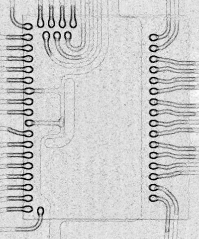
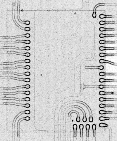
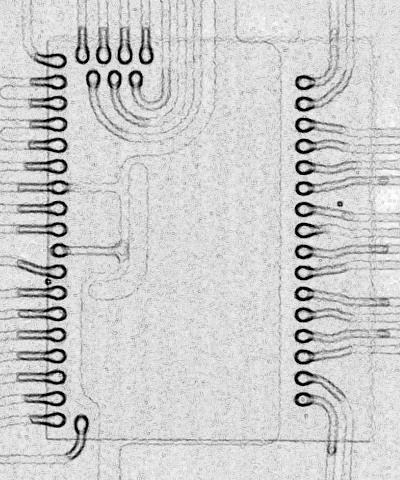
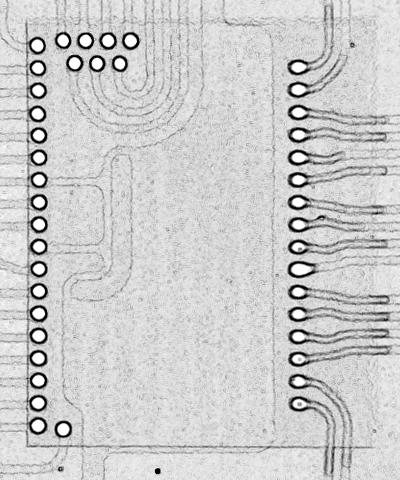
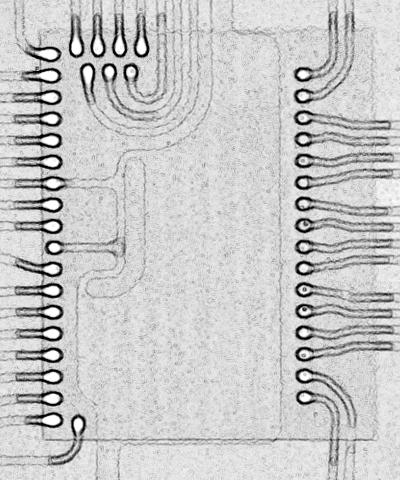
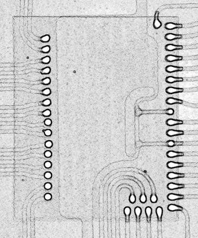
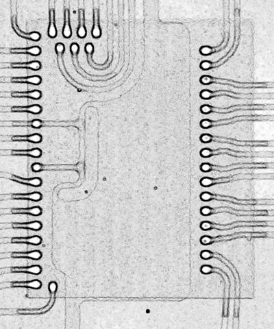
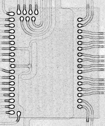
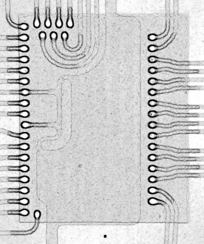
14 Soldering Performance X-ray Evaluation Technique 2-D x-ray, normal to surface Sobel filter applied Image inverted Normalize background density Yields information on wetting and bump mass
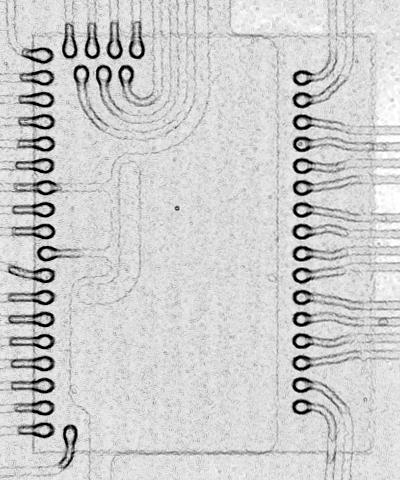
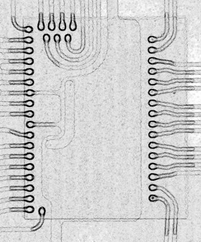
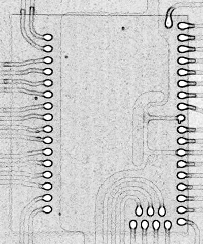
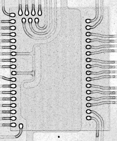
15 Soldering Performance Baseline Material KNORMAL KESTER 6 Placement Error Placement Error
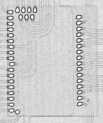
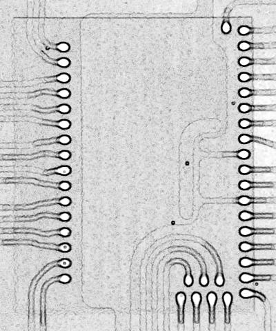
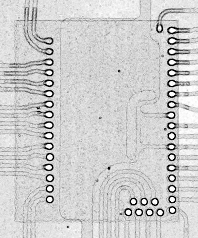
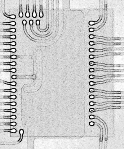
16 Soldering Performance KNORMAL KESTER 6 Rheology Controlled Material
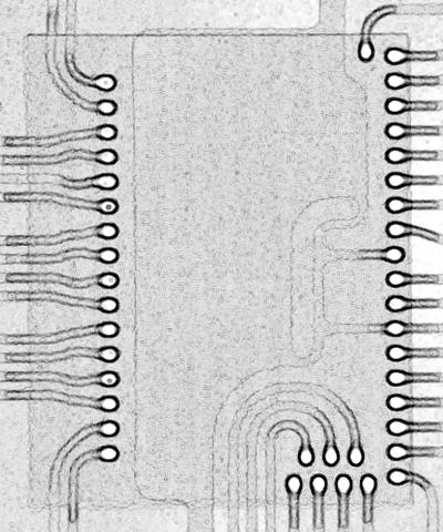
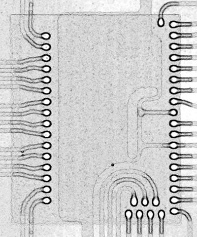
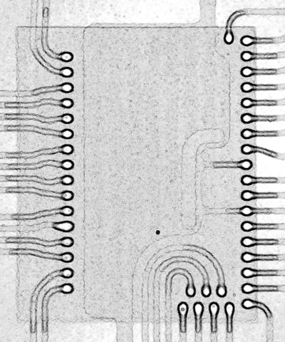
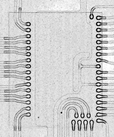
17 Soldering Performance KNORMAL KESTER 6 Bead Based Material Placement Error
18 Reliability Reliability Test Matrix
19 Reliability Summary Eutectic, bead-based materials have passed all reliability testing to date Thermal Cycle & Thermal Shock complete Awaiting final results BTH & HTOL tests near completion BTH, HTOL were passed previously using same resin system
20 Conclusions Anti-collapse technology incorporated in RE is most economical approach Eliminate need to incorporate substrate or die features to limit collapse Eliminate need for pad definition Two viable approaches to anti-collapse RE for FCOF have been demonstrated Bead-based control Rheology-based control
21 Conclusions Bead-based anti-collapse will be qualified for disc drive applications For Eutectic die, Q For Pb-free die, Q Rheology-based anti-collapse will also be pursued for the general market. Requires change of filler technology Provides the greatest application flexibility
Lead Free Solder for Flip Chip
 Lead Free Solder for Flip Chip Zhenwei Hou & R. Wayne Johnson Laboratory for Electronics Assembly & Packaging Auburn University 162 Broun Hall, ECE Dept. Auburn, AL 36489 USA 334-844-1880 johnson@eng.auburn.edu
Flip Chip - Integrated In A Standard SMT Process
 Flip Chip - Integrated In A Standard SMT Process By Wilhelm Prinz von Hessen, Universal Instruments Corporation, Binghamton, NY This paper reviews the implementation of a flip chip product in a typical
EPOXY FLUX MATERIAL AND PROCESS FOR ENHANCING ELECTRICAL INTERCONNECTIONS
 As originally published in the SMTA Proceedings. EPOXY FLUX MATERIAL AND PROCESS FOR ENHANCING ELECTRICAL INTERCONNECTIONS Neil Poole, Ph.D., Elvira Vasquez, and Brian J. Toleno, Ph.D. Henkel Electronic
Selection and Application of Board Level Underfill Materials
 Selection and Application of Board Level Underfill Materials Developed by the Underfill Materials Design, Selection and Process Task Group (5-24f) of the Assembly and Joining Committee (5-20) of IPC Supersedes:
Cost Analysis of Flip Chip Assembly Processes: Mass Reflow with Capillary Underfill and Thermocompression Bonding with Nonconductive Paste
 Cost Analysis of Flip Chip Assembly Processes: Mass Reflow with Capillary Underfill and Thermocompression Bonding with Nonconductive Paste Amy Palesko Lujan SavanSys Solutions LLC 10409 Peonia Court Austin,
One Step Chip Attach Materials (OSCA) for Conventional Mass Reflow Processing
 for Conventional Mass Reflow Processing") One Step Chip Attach Materials (OSCA) for Conventional Mass Reflow Processing Daniel J. Duffy 1, Lin Xin, Jean Liu, Bruno Tolla 2 Kester Inc. 800 West Thorndale Ave. Itasca, IL 60143, USA Ph: 630-616-4036
One Step Chip Attach Materials (OSCA) for Conventional Mass Reflow Processing Daniel J. Duffy 1, Lin Xin, Jean Liu, Bruno Tolla 2 Kester Inc. 800 West Thorndale Ave. Itasca, IL 60143, USA Ph: 630-616-4036
3D-WLCSP Package Technology: Processing and Reliability Characterization
 3D-WLCSP Package Technology: Processing and Reliability Characterization, Paul N. Houston, Brian Lewis, Fei Xie, Ph.D., Zhaozhi Li, Ph.D.* ENGENT Inc. * Auburn University ENGENT, Inc. 2012 1 Outline Packaging
Selective Flux Jetting Plays Key Role In the Optimization of Process Results For Advanced Packaging Applications
 Selective Flux Jetting Plays Key Role In the Optimization of Process Results For Advanced Packaging Applications Written for Advanced Packaging By Fabio Okada Over the past few years, many new production
BGA Package Underfilm for Autoplacement. Jan Danvir Tom Klosowiak
 BGA Package Underfilm for Autoplacement Jan Danvir Tom Klosowiak NIST-ATP Acknowledgment Project Brief Microelectronics Manufacturing Infrastructure (October 1998) Wafer-Scale Applied Reworkable Fluxing
Effects of Flux and Reflow Parameters on Lead-Free Flip Chip Assembly. Sandeep Tonapi 1 Doctoral Candidate
 Effects of Flux and Reflow Parameters on Lead-Free Flip Chip Assembly Sandeep Tonapi 1 Doctoral Candidate Peter Borgesen, Ph.D. 2 Manager, Area Array Consortium K. Srihari, Ph.D. 1 Professor, Department
TECHNOLOGIES FOR APPLYING FLUIDS IN SEMICONDUCTOR PACKAGING
 TECHNOLOGIES FOR APPLYING FLUIDS IN SEMICONDUCTOR PACKAGING Alec J. Babiarz Asymtek Carlsbad, CA, USA ajbabiarz@asymtek.com ABSTRACT Jetting fluids in semiconductor packaging and assembly has become an
Reliability And Processability Of Sn/Ag/Cu Solder Bumped Flip Chip Components On Organic High Density Substrates
 Reliability And Processability Of Sn/Ag/Cu Solder Bumped Flip Chip Components On Organic High Density Substrates Minja Penttilä, Kauppi Kujala Nokia Mobile Phones, Research and Technology Access Itamerenkatu
TC-3040 Thermally Conductive Gel. Product Briefing for 3DInCites Award Nomination
 TC-3040 Thermally Conductive Gel Product Briefing for 3DInCites Award Nomination TC-3040 Thermally Conductive Gel Material has been designed and optimized for high performance flip chip applications TC-3040
Basic PCB Level Assembly Process Methodology for 3D Package-on-Package
 Basic PCB Level Assembly Process Methodology for 3D Package-on-Package Vern Solberg STC-Madison Madison, Wisconsin USA Abstract The motivation for developing higher density IC packaging continues to be
Effect of Underfill Entrapment on the Reliability of Flip-Chip Solder Joint
 Y. C. Chan e-mail: eeycchan@cityu.edu.hk M. O. Alam K. C. Hung H. Lu C. Bailey EPA Centre, Department of Electronic Engineering, City University of Hong Kong, Hong Kong, China; School of Computing and
Flip Chip Assembly is as Easy as 1, 2, 3
 Flip Chip Assembly is as Easy as 1, 2, 3 Reliable estimates put total flip chip production volume at over one billion units for 2000. Most are being used today in low-priced consumer products, such as
World Academy of Science, Engineering and Technology International Journal of Electronics and Communication Engineering Vol:3, No:11, 2009
 International Science Index, Electronics and Communication Engineering waset.org/publication/5181 Effect of Curing Profile to Eliminate the Voids / Black Dots Formation in Underfill Epoxy for Hi-CTE Flip
Ultralow Residue Semiconductor Grade Fluxes for Copper Pillar Flip-Chip
 Ultralow Residue Semiconductor Grade Fluxes for Copper Pillar Flip-Chip SzePei Lim (Presenter), Jason Chou, Maria Durham, and Dr. Andy Mackie Indium Corporation 1 Outline of Presentation Roadmaps and challenges
Flip Chip Challenges
 Flip Chip Challenges By: Steve Bezuk, PH.D. General Manager, Applied Technology Development and Flip Chip Kyocera America, Inc. Introduction Flip Chip packaging has seen an explosive growth in recent years.
ROOM TEMPERATURE FAST FLOW REWORKABLE UNDERFILL FOR LGA
 As originally published in the SMTA Proceedings ROOM TEMPERATURE FAST FLOW REWORKABLE UNDERFILL FOR LGA Mary Liu, Ph.D., and Wusheng Yin, Ph.D. YINCAE Advanced Materials, LLC Albany, NY, USA wyin@yincae.com
Plasma for Underfill Process in Flip Chip Packaging
 Plasma for Underfill Process in Flip Chip Packaging Jack Zhao and James D. Getty Nordson MARCH 2470-A Bates Avenue Concord, California 94520-1294 USA Published by Nordson MARCH www.nordsonmarch.com 2015
Challenges in Material Applications for SiP
 Challenges in Material Applications for SiP Sze PeiLim Regional Product Manager for Semiconductor Products Indium Corporation Indium Corporation Materials Supplier: SMT solder pastes and fluxes Power semiconductor
A NOVEL HIGH THERMAL CONDUCTIVE UNDERFILL FOR FLIP CHIP APPLICATION
 A NOVEL HIGH THERMAL CONDUCTIVE UNDERFILL FOR FLIP CHIP APPLICATION YINCAE Advanced Materials, LLC WHITE PAPER November 2013 2014 YINCAE Advanced Materials, LLC - All Rights Reserved. YINCAE and the YINCAE
Technology Drivers for Plasma Prior to Wire Bonding
 Technology Drivers for Plasma Prior to Wire Bonding James D. Getty Nordson MARCH Concord, CA, USA info@nordsonmarch.com Technology Drivers for Plasma Prior to Wire Bonding Page 1 ABSTRACT Advanced packaging
WS-575-C-RT. Halogen-Free Ball-Attach Flux PRODUCT DATA SHEET
 -RT Halogen-Free Ball-Attach Introduction Indium Corporation s Ball-Attach -RT allows customers to use a completely halogen-free (NIA = no intentionally added halogens) single-step ball-attach process
Characteristics of Solder Paste
 Characteristics of Solder Paste Flow Solder paste is a viscous non-newtonian fluid, whose resistance to flow is not constant, and which exhibits shear thinning. This is an essential requirement for printing,
FLIP CHIP ON ORGANIC SUBSTRATES
 FLIP CHIP ON ORGANIC SUBSTRATES Peter Borgesen Universal Instruments Corporation Binghamton, NY ABSTRACT The attachment of a flip chip of moderate size and pitch to an organic substrate has lost much of
Recent Advances in Die Attach Film
 Recent Advances in Die Attach Film Frederick Lo, Maurice Leblon, Richard Amigh, and Kevin Chung. AI Technology, Inc. 70 Washington Road, Princeton Junction, NJ 08550 www.aitechnology.com Abstract: The
Advanced Analytical Techniques for Semiconductor Assembly Materials and Processes. Jason Chou and Sze Pei Lim Indium Corporation
 Advanced Analytical Techniques for Semiconductor Assembly Materials and Processes Jason Chou and Sze Pei Lim Indium Corporation Agenda Company introduction Semiconductor assembly roadmap challenges Fine
High Reliable Non-Conductive Adhesives for Flip Chip CSP Applications
 High Reliable Non-Conductive Adhesives for Flip Chip CSP Applications Myung-Jin Yim, Jin-Sang Hwang ACA/F Div., Telephus Co. 25-11, Jang-dong, Yusong-gu,, Taejon 35-71, Korea Tel.: +82-42-866-1461, Fax:
ELECTRICALLY CONDUCTIVE DIE ATTACH ADHESIVE
 ABLEBOND 84-1LMISR4 ELECTRICALLY CONDUCTIVE DIE ATTACH ADHESIVE DESCRIPTION Ablebond 84-1LMISR4 electrically conductive die attach adhesive has been formulated for use in high throughput, automatic die
Minimizing Voiding. Cristian Tudor Applications Engineer Eastern Europe
 Minimizing Voiding Cristian Tudor Applications Engineer Eastern Europe ctudor@indium.com INDIUM CORPORATION 1 Indium Corporation s Business We develop, manufacture, market and support solders, electronics
Lead Free Surface Mount Technology. Ian Wilding BSc Senior Applications Engineer Henkel Technologies
 Lead Free Surface Mount Technology Ian Wilding BSc Senior Applications Engineer Henkel Technologies Overview of the Presentation First contact: Impact on the production operator Packaging Labelling Impact
Bridging Supply Chain Gap for Exempt High-Reliability OEM s
 Bridging Supply Chain Gap for Exempt High-Reliability OEM s Hal Rotchadl hrotchadl@premiers2.com www.premiers2.com Premier Semiconductor Services Tempe, AZ RoHS exempt high reliability OEMs breathed a
Manufacturing and Reliability Modelling
 Manufacturing and Reliability Modelling Silicon Chip C Bailey University of Greenwich London, England Printed Circuit Board Airflow Temperature Stress at end of Reflow Stress Product Performance in-service
EXTRA FINE PITCH FLIP CHIP ASSEMBLY PROCESS, UNDERFILL EVALUATION AND RELIABILITY
 As originally published in the SMTA Proceedings EXTRA FINE PITCH FLIP CHIP ASSEMBLY PROCESS, UNDERFILL EVALUATION AND RELIABILITY Fei Xie, Ph.D. *, Daniel F. Baldwin, Ph.D. *, Han Wu *, Swapon Bhattacharya,
RECOMMENDED ELECTRONIC ASSEMBLY MATERIALS
 RECOMMENDED ELECTRONIC ASSEMBLY MATERIALS MATERIALS AND PEOPLE THAT DRIVE INNOVATION Kester is a leading innovator and global supplier of premium electronic assembly materials that services the automotive,
Dam and Fill Encapsulation for Microelectronic Packages
 Dam and Fill Encapsulation for Microelectronic Packages Steven J. Adamson, Christian Q. Ness Asymtek 2762 Loker Avenue West Carlsbad, CA 92008 Tel: 760-431-1919; Fax: 760-930-7487 Email: info@asymtek.com;
WF6317. A superactive low-volatile/high heat-resistant water-soluble flux for ball soldering
 WF637 A superactive low-volatile/high heat-resistant water-soluble flux for ball soldering Low viscosity and high tacking power stabilize ball holding force and ensures excellent solder wettability Easy
White Paper Quality and Reliability Challenges for Package on Package. By Craig Hillman and Randy Kong
 White Paper Quality and Reliability Challenges for Package on Package By Craig Hillman and Randy Kong Background Semiconductor technology advances have been fulfilling Moore s law for many decades. However,
room and cold readouts were performed every 250 cycles. Failure data and Weibull plots were generated. Typically, the test vehicles were subjected to
 SOLDER JOINT RELIABILITY ASSESMENT OF Sn-Ag-Cu BGA COMPONENTS ATTACHED WITH EUTECTIC Pb-Sn SOLDER Fay Hua 1, Raiyo Aspandiar 2, Cameron Anderson 3, Greg Clemons 3, Chee-key Chung 4, Mustapha Faizul 4 Intel
Flip Chip Bump Electromigration Reliability: A comparison of Cu Pillar, High Pb, SnAg, and SnPb Bump Structures
 Flip Chip Bump Electromigration Reliability: A comparison of Cu Pillar,,, and SnPb Bump Structures Ahmer Syed, Karthikeyan Dhandapani, Lou Nicholls, Robert Moody, CJ Berry, and Robert Darveaux Amkor Technology
High Density PoP (Package-on-Package) and Package Stacking Development
 and Package Stacking Development") High Density PoP (Package-on-Package) and Package Stacking Development Moody Dreiza, Akito Yoshida, *Kazuo Ishibashi, **Tadashi Maeda, Amkor Technology Inc. 1900 South Price Road, Chandler, AZ 85248, U.S.A.
High Density PoP (Package-on-Package) and Package Stacking Development Moody Dreiza, Akito Yoshida, *Kazuo Ishibashi, **Tadashi Maeda, Amkor Technology Inc. 1900 South Price Road, Chandler, AZ 85248, U.S.A.
Material Selection and Parameter Optimization for Reliable TMV Pop Assembly
 Selection and Parameter Optimization for Reliable TMV Pop Assembly Brian Roggeman, David Vicari Universal Instruments Corp. Binghamton, NY, USA Roggeman@uic.com Martin Anselm, Ph.D. - S09_02.doc Lee Smith,
Microelectronic Materials CATALOG
 Microelectronic Materials CATALOG LORD partners with customers to leverage expertise in multiple chemistries and diverse applications to develop customized solutions. Design Without Compromise At LORD,
LS720V Series. Comparison of crack progression between Sn-Cu-Ni-Ge and M773. Development of Ag-free/M773 alloy
 LS72V Series Low-Ag/Ag-free solder pastes with lower void Reduces voids by improving fluidity of flux during solder melting Reduces voids even in bottom surface electrode type components by improving solder
HOW THE MOLD COMPOUND THERMAL EXPANSION OVERRULES THE SOLDER COMPOSITION CHOICE IN BOARD LEVEL RELIABILITY PERFORMANCE
 HOW THE MOLD COMPOUND THERMAL EXPANSION OVERRULES THE SOLDER COMPOSITION CHOICE IN BOARD LEVEL RELIABILITY PERFORMANCE AUTHORS: B. VANDEVELDE, L. DEGRENDELE, M. CAUWE, B. ALLAERT, R. LAUWAERT, G. WILLEMS
ALPHA OM-5100 FINE PITCH SOLDER PASTE
 SM 797-7 ALPHA OM-5100 FINE PITCH SOLDER PASTE DESCRIPTION Cookson Electronics Assembly Material s ALPHA OM-5100, is a low residue, no-clean solder paste designed to maximize SMT line yields. The flux
Microelectronic Materials. Catalog
 Microelectronic Materials Catalog LORD partners with customers to leverage expertise in multiple chemistries and diverse applications to develop customized solutions. Design Without Compromise At LORD,
Packaging Effect on Reliability for Cu/Low k Damascene Structures*
 Packaging Effect on Reliability for Cu/Low k Damascene Structures* Guotao Wang and Paul S. Ho Laboratory of Interconnect & Packaging, TX 78712 * Work supported by SRC through the CAIST Program TRC 2003
IBM Research Report. The Over-Bump Applied Resin Wafer-Level Underfill Process: Process, Material and Reliability
 RC24851 (W0908-142) August 31, 2009 Other IBM Research Report The Over-Bump Applied Resin Wafer-Level Underfill Process: Process, Material and Reliability Claudius Feger, Nancy LaBianca, Michael Gaynes,
YOUR Strategic TESTING ENGINEERING CONCEPT SMT FLIP CHIP PRODUCTION OPTO PACKAGING PROCESS DEVELOPMENT CHIP ON BOARD SUPPLY CHAIN MANAGEMENT
 YOUR Strategic TECHNOLOGY PARTNER Wafer Back-End OPTO PACKAGING PROCESS DEVELOPMENT CONCEPT FLIP CHIP PROTOTYping ENGINEERING TESTING SMT PRODUCTION CHIP ON BOARD SUPPLY CHAIN MANAGEMENT Next Level 0f
Flip-Chip Underfill: Materials, Process and Reliability
 Flip-Chip Underfill: Materials, Process and Reliability Zhuqing Zhang 1, PhD and C.P. Wong 2, PhD 1 Hewlett-Packard Company, Corvallis, OR 97330 2 School of Materials Science and Engineering & Packaging
NEW GENERATION UNDERFILLS POWER THE 2 ND FLIP CHIP REVOLUTION
 NEW GENERATION UNDERFILLS POWER THE 2 ND FLIP CHIP REVOLUTION Dr. Ken Gilleo ET-Trends; gilleo@ieee.org (previously, Cookson Electronics Group Abstract Various forms of Flip Chip technology have been around
Optimizing the Assembly Process with Cure-On-Demand UV/Visible Light-Curable Adhesives
 Optimizing the Assembly Process with Cure-On-Demand UV/Visible Light-Curable Adhesives Virginia P. Read Industrial Market Segment Manager DYMAX Corporation Torrington, CT www.dymax.com Introduction Manufacturers
Development of New No-Flow Underfill Materials for Both Eutectic Sn-Pb Solder and a High Temperature Melting Lead-Free Solder
 466 IEEE TRANSACTIONS ON COMPONENTS AND PACKAGING TECHNOLOGIES, VOL. 26, NO. 2, JUNE 2003 Development of New No-Flow Underfill Materials for Both Eutectic Sn-Pb Solder and a High Temperature Melting Lead-Free
Edge Bond Package joint reinforcement JU-120EB Product Information
 www.ko-ki.co.jp #55023 First issue on October 25, 2017 Revised on Koki Adhesive Edge Bond Package joint reinforcement Product Information BGA body Disclaimer This Product Information contains product performance
Cree EZ-p LED Chips Handling and Packaging Recommendations
 Cree EZ-p LED Chips Handling and Packaging Recommendations INTRODUCTION This application note provides the user with an understanding of Cree s EZ-p p-pad up (anode up) LED devices, as well as recommendations
Assembly and Rework of Lead Free Package on Package Technology By: Raymond G. Clark and Joseph D. Poole TT Electronics - IMS Perry, Ohio
 Assembly and Rework of Lead Free Package on Package Technology By: Raymond G. Clark and Joseph D. Poole TT Electronics - IMS Perry, Ohio Abstract: Miniaturization continues to be a driving force in both
Welcome to SMTA Brazil Chapter Brook Sandy-Smith Dr. Ron Lasky Tim Jensen
 Welcome to SMTA Brazil Chapter 2013 Presented by Authors Ivan Castellanos Edward Briggs Brook Sandy-Smith Dr. Ron Lasky Tim Jensen Advantages / Concerns HP testing Mechanical properties New work Area ratio
Development of No-Flow Underfill Materials for Lead-Free Solder Bumped Flip-Chip Applications
 IEEE TRANSACTIONS ON COMPONENTS AND PACKAGING TECHNOLOGIES, VOL. 24, NO. 1, MARCH 2001 59 Development of No-Flow Underfill Materials for Lead-Free Solder Bumped Flip-Chip Applications Z. Q. Zhang, S. H.
Thermo-Mechanical FEM Analysis of Lead Free and Lead Containing Solder for Flip Chip Applications
 Thermo-Mechanical FEM Analysis of Lead Free and Lead Containing Solder for Flip Chip Applications M. Gonzalez 1, B. Vandevelde 1, Jan Vanfleteren 2 and D. Manessis 3 1 IMEC, Kapeldreef 75, 3001, Leuven,
Complete Solder Solutions
 Complete Solder Solutions A NORDSON COMPANY 1 Our Vision EFD Solder Paste Group is the service leader in the solder dispensing market, delivering integrated process solutions through best-in-class performance
Thermal Management Solutions for Automotive, Lighting and Industrial Applications
 Thermal Management Solutions for Automotive, Lighting and Industrial Applications UL Prospector Webinar, January 25, 2018 Presented by Florian Damrath & Julien Renaud Technical Service & Development, Advanced
Xilinx CN Package Qualification Updates for MRQW 2015 Kangsen Huey Space Product Marketing Manager January, 2014
 Xilinx CN Package Qualification Updates for MRQW 2015 Kangsen Huey Space Product Marketing Manager January, 2014 CF (IBM) vs CN (Kyocera) Packages Page 2 Comparison between IBM (CF) and Kyocera (CN) Packages
TRADITIONALLY, epoxy based encapsulants are filled
 54 IEEE TRANSACTIONS ON ADVANCED PACKAGING, VOL. 22, NO. 1, FEBRUARY 1999 Comparative Study of Thermally Conductive Fillers for Use in Liquid Encapsulants for Electronic Packaging C. P. Wong, Fellow, IEEE,
3D FRACTURE MECHANICS ANALYSIS OF UNDERFILL DELAMINATION FOR FLIP CHIP PACKAGES
 3D FRACTURE MECHANICS ANALYSIS OF UNDERFILL DELAMINATION FOR FLIP CHIP PACKAGES Zhen Zhang, Charlie J Zhai, and Raj N Master Advanced Micro Devices, Inc. 1050 E. Arques Ave., Sunnyvale, CA 94085, USA Phone:
3D Package Technologies Review with Gap Analysis for Mobile Application Requirements. Apr 22, 2014 STATS ChipPAC Japan
 3D Package Technologies Review with Gap Analysis for Mobile Application Requirements Apr 22, 2014 STATS ChipPAC Japan T.Nishio Contents Package trends and roadmap update Advanced technology update Fine
McKinney, Texas. McKinney, Texas, Cheshire, CT, Morrisville, NC USA
 McKinney, Texas McKinney, Texas, Cheshire, CT, Morrisville, NC USA http://www.m-coat.com Just like an old friend, we can do it all Military Microelectronics Electronics Medical Conductive silvers Encapsulants
Development of a Fluxless Flip Chip Bonding Process for Optical Military Electronics
 Development of a Fluxless Flip Chip Bonding Process for Optical Military Electronics Michael Girardi, Daric Laughlin, Philip Abel, Steve Goldammer, John Smoot NNSA s Kansas City Plant managed by Honeywell
INTERFLUX ELECTRONICS NV
 Reflow soldering temperature profiling Min : 30sec Max : 120sec Max : +4 C/sec Max : 250 C Min : 230 C Min: +0,5 C/sec Min : +1 C/sec Max : +3 C/sec Max : +1 C/sec Max : -6 C/sec Min : -2 C/sec Min : +1
Optoelectronic Chip Assembly Process of Optical MCM
 2017 IEEE 67th Electronic Components and Technology Conference Optoelectronic Chip Assembly Process of Optical MCM Masao Tokunari, Koji Masuda, Hsiang-Han Hsu, Takashi Hisada, Shigeru Nakagawa, Science
Bob Willis Process Guides
 Practical Selection/Problems with SMT Adhesives Bob Willis Surface M ount Technology (SM T) first started with the introduction of mixed technology designs incorporating components mounted on the underside
ENHANCING MECHANICAL SHOCK PERFORMANCE USING EDGEBOND TECHNOLOGY
 ENHANCING MECHANICAL SHOCK PERFORMANCE USING EDGEBOND TECHNOLOGY Steven Perng, Tae-Kyu Lee, and Cherif Guirguis Cisco Systems, Inc. San Jose, CA, USA sperng@cisco.com Edward S. Ibe Zymet, Inc. East Hanover,
Reliability of Lead-Free Solder Connections for Area-Array Packages
 Presented at IPC SMEMA Council APEX SM 2001 For additional information, please email marketing@amkor.com Reliability of Lead-Free Solder Connections for Area-Array Packages Ahmer Syed Amkor Technology,
TRANSFER MOULDING & EPOXY MOULD COMPOUND TECHNOLOGY WORKSHOP
 TRANSFER MOULDING & EPOXY MOULD COMPOUND TECHNOLOGY WORKSHOP TRANSFER MOULDING & EPOXY MOULD COMPOUND TECHNOLOGY WORKSHOP INTRODUCTION This workshop will provide participants with knowledge and understanding
Lead-Free Solder Bump Technologies for Flip-Chip Packaging Applications
 Lead-Free Solder Bump Technologies for Flip-Chip Packaging Applications Zaheed S. Karim 1 and Jim Martin 2 1 Advanced Interconnect Technology Ltd. 1901 Sunley Centre, 9 Wing Yin Street, Tsuen Wan, Hong
Assembly Challenges in Developing 3D IC Package with Ultra High Yield and High Reliability
 Assembly Challenges in Developing 3D IC Package with Ultra High Yield and High Reliability Raghunandan Chaware, Ganesh Hariharan, Jeff Lin, Inderjit Singh, Glenn O Rourke, Kenny Ng, S. Y. Pai Xilinx Inc.
Anisotropic Conductive Adhesives with Enhanced Thermal Conductivity for Flip Chip Applications
 Anisotropic Conductive Adhesives with Enhanced Thermal Conductivity for Flip Chip Applications Myung-Jin Yim, Jin-Sang Hwang and Jin-Gu Kim ACA/F Dept., Telephus, Inc. 25-11, Jang-dong, Yusong-gu, Taejon
EP A2 (19) (11) EP A2 (12) EUROPEAN PATENT APPLICATION. (43) Date of publication: Bulletin 2006/23
 (11) EP A2 (12) EUROPEAN PATENT APPLICATION. (43) Date of publication: Bulletin 2006/23") (19) Europäisches Patentamt European Patent Office Office européen des brevets (12) EUROPEAN PATENT APPLICATION (11) EP 1 667 226 A2 (43) Date of publication: 07.06.06 Bulletin 06/23 (1) Int Cl.: H01L
(19) Europäisches Patentamt European Patent Office Office européen des brevets (12) EUROPEAN PATENT APPLICATION (11) EP 1 667 226 A2 (43) Date of publication: 07.06.06 Bulletin 06/23 (1) Int Cl.: H01L
Application of Spacer Filled Silicone Die Adhesive in Stacked Chip Technology
 Application of Spacer Filled Silicone Die Adhesive in Stacked Chip Technology Xuan Li, R. Wayne Johnson 200 Broun Hall, Auburn University, Auburn, Alabama 36849 lixuan1@eng.auburn.edu Johnson@eng.auburn.edu
Tombstoning, Beading & Ultra-Fine Pitch Issues. Harry Trip Cobar Europe BV, Holland
 Tombstoning, Beading & Ultra-Fine Pitch Issues Harry Trip Cobar Europe BV, Holland Tombstoning What is it? The partial or complete erection of passive SMT-components Picture: Courtesy Fraunhofer ISIT Institute
Epoxy. Epoxy 90, ,000. Epoxy. Epoxy. low ion content, Encapsulation of electronic
 - - and Light Curing Adhesives Our comprehensive range of systems covers a multitude of applications and offers many advantages: systems are used in many fields in both trade and industry. adhesives and
Selector Guide. Providing the Connections for your Success. Automotive ele c tronics
 Providing the Connections for your Success Selector Guide Automotive ele c tronics Conductive Adhesives - Materials for Harsh Environment Protection - Underfill Encapsulants Electrically Conductive Adhesives
RELIABILITY IMPACT OF COPPER-DOPED EUTECTIC TIN-LEAD BUMP AND ITS VOIDING UPON FLIP CHIP ASSEMBLIES
 RELIABILITY IMPACT OF COPPER-DOPED EUTECTIC TIN-LEAD BUMP AND ITS VOIDING UPON FLIP CHIP ASSEMBLIES David Ihms and Shing Yeh Delphi Electronics & Safety Kokomo, IN, USA david.w.ihms@delphi.com and shing.yeh@delphi.com
Board Assembly Roadmap
 Board Assembly Roadmap Speaker & Chair: Dr. Dongkai Shangguan (Flextronics) Co-chair: Dr. Ravi Bhatkal (Cookson) Co-chair: David Geiger (Flextronics) Agenda Roadmap Development Approach Chapter Overview
Board Assembly Roadmap. TWG Chair: Dr. Dongkai Shangguan (Flextronics) Co-chair: Dr. Ravi Bhatkal (Cookson) Co-chair: David Geiger (Flextronics)
 Co-chair: Dr. Ravi Bhatkal (Cookson) Co-chair: David Geiger (Flextronics)") Board Assembly Roadmap TWG Chair: Dr. Dongkai Shangguan (Flextronics) Co-chair: Dr. Ravi Bhatkal (Cookson) Co-chair: David Geiger (Flextronics) Agenda Roadmap Development Approach Participants Key Trends
Board Assembly Roadmap TWG Chair: Dr. Dongkai Shangguan (Flextronics) Co-chair: Dr. Ravi Bhatkal (Cookson) Co-chair: David Geiger (Flextronics) Agenda Roadmap Development Approach Participants Key Trends
Illuminating Innovations
 Illuminating Innovations TM Silicone Solutions for LED Packaging Emir Debastiani Application Engineer Dow Corning Brazil Email: emir.debastiani@dowcorning.com Table of Contents Dow Corning Introduction
JOINT INDUSTRY STANDARD
 JOINT INDUSTRY STANDARD AUGUST 1999 Semiconductor Design Standard for Flip Chip Applications ASSOCIATION CONNECTING ELECTRONICS INDUSTRIES Semiconductor Design Standard for Flip Chip Applications About
Guidelines for Vishay Sfernice Resistive and Inductive Components
 VISHAY SFERNICE www.vishay.com Resistive and Inductive Products By Pascale Nagy Caution: Information included in product datasheets are ing to the general information given in this 1. STORAGE RECOMMENDATION
YOUR Strategic TESTING ENGINEERING CONCEPT SMT FLIP CHIP PRODUCTION OPTO PACKAGING PROCESS DEVELOPMENT CHIP ON BOARD SUPPLY CHAIN MANAGEMENT
 YOUR Strategic TECHNOLOGY PARTNER Wafer Back-End OPTO PACKAGING PROCESS DEVELOPMENT CONCEPT FLIP CHIP PROTOTYping ENGINEERING TESTING SMT PRODUCTION CHIP ON BOARD SUPPLY CHAIN MANAGEMENT Next Level 0f
TEMPERATURE CYCLING AND FATIGUE IN ELECTRONICS
 TEMPERATURE CYCLING AND FATIGUE IN ELECTRONICS Gilad Sharon, Ph.D. DfR Solutions Beltsville, MD, USA gsharon@dfrsolutions.com Greg Caswell DfR Solutions Liberty Hill, TX, USA gcaswell@dfrsolutions.com
DITF ToolKit 1. Standard Substrate Sizes (selected at the factory for optimum process)
") DITF ToolKit 1 DITF Toolkit Substrates Common Substrate Materials Alumina (99.5% min) єr = 9.9 Tan d = 1.5 x10⁻⁴ Aluminum Nitride (K170) єr = 8.9 Tan d = 2.0 x10⁻³ Beryllia (99.5%) єr = 6.7 Tan d = 3.0
DITF ToolKit 1 DITF Toolkit Substrates Common Substrate Materials Alumina (99.5% min) єr = 9.9 Tan d = 1.5 x10⁻⁴ Aluminum Nitride (K170) єr = 8.9 Tan d = 2.0 x10⁻³ Beryllia (99.5%) єr = 6.7 Tan d = 3.0
Gap Filler Liquid Dispensed Materials
 26 Thermal Interface Selection Guide Gap Filler Liquid Dispensed Materials Introduction Effective thermal management is key to ensuring consistent performance and long-term reliability of many electronic
Next Gen Packaging & Integration Panel
 Next Gen Packaging & Integration Panel ECTC 2012 Daniel Tracy, Sr. Director Industry Research & Statistics SEMI May 29, 2012 Packaging Supply Chain Market Trends Material Needs and Opportunities Market
Fixed Resistors INSULATED ALUMINUM SUBSTRATES. Thermal Solutions for Hi Brightness LED Applications - Application Note
 INSULATED ALUMINUM SUBSTRATES TT electronics is a leading designer and manufacturer of electronic components. As a result of our experience with power components, Anotherm substrates were developed as
In this section we take reference to the questionnaire i from OEKO Institute published on May 29 th Abbreviations and Definitions
 9 th Adaptation to scientific and technical progress of Exemptions 8(e), 8(f)(b), 8(g), 8(j) and 14 of Annex II to Directive 2000/53/EC (ELV), Stakeholder Consultation Questionnaire Application for a continuation
Thermal Residue Fingerprinting: A Revolutionary Approach to Develop a Selective Cleaning Solution
 Thermal Residue Fingerprinting: A Revolutionary Approach to Develop a Selective Cleaning Solution Steve Stach, Austin American Technology Harald Wack, Ph.D., Umut Tosun, Naveen Ravindran, ZESTRON America,
Building HDI Structures using Thin Films and Low Temperature Sintering Paste
 Building HDI Structures using Thin Films and Low Temperature Sintering Paste Catherine Shearer, James Haley and Chris Hunrath Ormet Circuits Inc. - Integral Technology California, USA chunrath@integral-hdi.com
Gap Filler 1000 (Two-Part)
") Gap Filler 1000 (Two-Part) Thermally Conductive, Liquid Gap Filling Material Thermal conductivity: 1.0 W/m-K Ultra-conforming, designed for fragile and low-stress applications Ambient and accelerated cure
Gap Filler 1000 (Two-Part) Thermally Conductive, Liquid Gap Filling Material Thermal conductivity: 1.0 W/m-K Ultra-conforming, designed for fragile and low-stress applications Ambient and accelerated cure