Supporting informations
|
|
|
- Hubert Lawrence
- 6 years ago
- Views:
Transcription
1 Supporting informations Microfluidic with integrated microfilter of conical-shaped holes for high efficiency and high purity capture of circulating tumor cells Yadong Tang 1+, Jian Shi 2+, Sisi Li 1, Li Wang 3, Yvon E.Cayre 2,4 and Yong Chen 1,5,6 * 1 Ecole Normale Supérieure-PSL Research University, Département de Chimie, Sorbonne Universités - UPMC Univ Paris 06, CNRS UMR 8640 PASTEUR, 24, rue Lhomond, Paris, France 2 BiocareCell, 249, rue Saint-Denis, Paris, France 3 Curie Institute, 12 rue Lhomond, Paris, France 4 Sorbonne Universités - UPMC Univ Paris 06, 4 place Jussieu Paris, France 5 Institute for Integrated Cell-Material Science, Kyoto University, Kyoto , Japan 6 Institute for Interdisciplinary Research, Jianghan University, Wuhan, China +Authors contributed equally to this work *Corresponding author: yong.chen@ens.fr 1
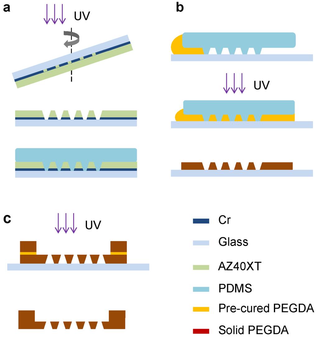
2 Supplementary Methods Fabrication of PEGDA microfilters The fabrication procedure of PEGDA microfilter is shown in Supplementary Fig.S1. Briefly, chromium mask of holes arrays of 5.5, 6.5, 8.0 μm diameter and 30 µm period was produced by micro pattern generator (μpg 101, Heidelberg Instruments). 30 µm AZ40XT resist layer was spin-coated on the mask and backside exposed with UV light at an incident angle of 20 (for a final of half conical angle of 13 ) and a rotation speed of 3 rpm. After development, conical holes of bottom and top diameters of 5.5, 6.5, 8.0μm and 19.4, 20.4, 21.9 μm were obtained, followed by evaporation of TMCS for anti-sticking surface treatment. A PDMS solution was prepared using GE RTV 615 PDMS components A and B at a ratio of 10:1 and then poured on the top of the resist master. After curing at 80 C for 2 h, the PDMS layer was peeled off and placed on a glass slide. Then, the PDMS-glass assembly was placed in a desiccator for degasing during 15 min. Meanwhile, a PEGDA solution mixed with 1v/v%2-hydroxy-2-methylpropiophenone as photo-initiator was prepared and used to fill the PDMS-glass cavity by degasing induced micro-aspiration, followed by UV exposure at 9.1mW/cm 2 for 30s. Finally, the solidified PEGDA filter was peeled off, resulting in a microfilter with conical holes and a porosity of 3.6%. To increase the mechanical strength, 100 µm thick PEGDA rings of 13 mm outer diameter and 6 or 9 mm inner diameter were prepared in a similar manner. Briefly, a 100 µm thick SU resist was exposed with a Cr mask defining the ring geometry. After development and trimethylchlorosilane (TMCS) evaporation, the PDMS mold was produced by soft lithography and placed on a glass slide. Then, the PEGDA solution was injected into the mold and solidified by UV exposure. Finally, the ring was mounted on the filter, using pre-cured PEGDA solution as 2
3 binder for UV curing. For comparison, filters of cylindrical holes were obtained using UV lithography at normal incident angle without rotation. Integration of PEGDA filter into microfluidic devices The layouts of the upper and bottom PDMS layers are shown in Supplementary Fig.S2. Here the upper PDMS was produced by soft lithography with a mold fabricated by a CNC milling system. First, a two level pattern was produced on a PMMA plate. The first level is a cavity of 13 mm diameter and 130 µm in depth, designed for embedment of PEGDA filter. The second level includes a 6 mm or 9 mm chamber, 8 radial channels of 400 µm width, the inlet, the outlet and the ring channels of 1 mm width, all having a depth of 400 µm. After machining, the mold was ultrasonic washed with isopropanol. Then, the pattern was replicated twice into PDMS by soft lithography and both inlet and outlet holes were punched, resulting in the desired upper layer. The bottom was fabricated by standard soft lithography with a mold fabricated by UV lithography. First, a chromium mask was produced and then replicated into a 100 µm thick photoresist (SU8-3050, Micro resist). After development and evaporation of TMCS, PDMS was poured on the SU8 mold with a thickness of ~ 1 mm and cured at 80 C for 1 h. After peeling off, the main chamber of diameter of 6 mm or 9 mm was punched. The surfaces of upper and bottom PDMS layers were treated by plasma shortly and the PEGDA filter was sandwiched between the two PDMS layer, following by a thermal bonding at 80 C for 30 min. Finally, the inlet and outlet of the bottom later were punched and the PDMS-PEGDA assembly was irreversibly bonded to a glass slide after plasma treatment of the PDMS later. 3
4 Hydrodynamic simulation Numerical simulation has been performed with commercial software (COMSOL Multiphysics). For simplicity, cylindrical- and conical-holes were replaced by a linear array of rectangular or trapezoidal slits, respectively, keeping the other geometrical parameters as the same of two-dimensional filters (6.5 µm entrance size, 30 µm thickness, and 30 µm pitch size). The results were obtained with a transfilter pressure of 100 Pa and water viscosity of without cells. Figure S7 shows the flow velocity over the interesting area, indicating a higher flow rate across the conical holes than across the cylindrical ones. Streamlines are also shown, illustrating a flow focusing effect, i.e., no flow goes to the areas at equidistance of neighboring holes. Definition of capture efficiency, WBC clearance efficiency and cell viability The capture efficiency of the device for the targeting tumor cells was defined as the ratio of tumor cells found on the filter,, to the initial tumor cells injected into the device,, (S1) The leukocyte clearance efficiency of the filter was defined as the ratio of the number of unclogged holes,, and the number of total holes of the filter,, per milliliter blood sample (S2) where is the number WBCs found on the filter. The cell viability of the tumor cells captured by the filter was defined as the ratio of live tumor cells,, and dead tumor cells, both being found on the filter 4
5 (S3) 5
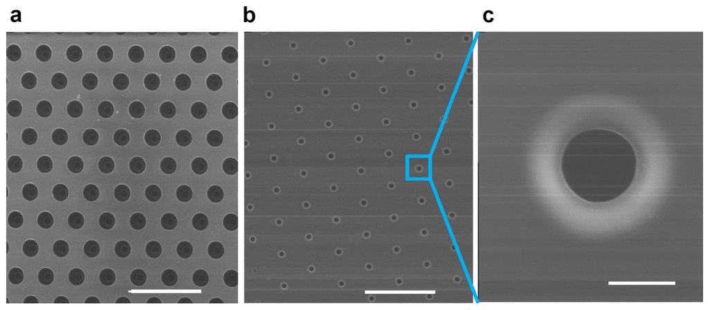
6 Supplementary Figure S1. Fabrication procedure of conical-hole filters. (a) Fabrication of PDMS mold with conical pillars; (b) Replication of PDMA pattern into PEGDA thin membrane, the same replication process is used for the fabrication of PEGDA ring; (c) UV assisted bonding of PEGDA membrane and ring. Supplementary Figure S2. Layout for the fabrication of upper (a) and bottom (b) PDMS layers. The filter is sandwiched between the PDMS layers and the sample is loaded from inlet 1 and collected from outlet 2, passing through the radical channels for cross-flow injection and then the filter for tumor cell capture. Supplementary Figure S3. PEGDA filter with conical-hole array. (a, b) Bottom and top view of SEM images of conical-hole array, respectively; (c) Top view SEM image of a single conical hole. Scale bar: (a, b) 100 µm (c) 5 µm. Supplementary Figure S4. Fluorescence images of WBCs isolated from a healthy donor on the filter. (a) Fluorescence of nuclei staining with DAPI (blue). (b, c) Fluorescence after staining with anti-ck-alexafluor 488 (green) and anti-cd45-pe (red), respectively. (d) Merge image of (a-c). Scale bar: (a-d) 30 µm. Supplementary Figure S5. Fluorescence images of WBCs on the filter. Blood samples of a healthy person were diluted in PBS at 1:1 (v/v%). After filtration and anti-cd45 staining, 6
7 fluorescence images were taken, showing a much reduced WBC retention by conical holes (a) than cylindrical ones (b). Scale bar: 100 μm. Supplementary Figure S6. SEM image of tumor cells on the filter. HT-29 cells were spiked in PBS at a 10 4 cells/ml concentration. After filtration, cells were fixed by dehydration and coated by 2nm thick gold. Scale bar: 100µm. Supplementary Figure S7. Hydrodynamic simulation of flow focusing. The same transfilter pressure (100 Pa) were applied, showing both flow focusing but a higher flow rate through trapezoidal slits than through rectangular ones. 7
8 Supplementary Figure S1 8
9 Supplementary Figure S2 9
10 Supplementary Figure S3 10

11 Supplementary Figure S4 11

12 Supplementary Figure S5 12
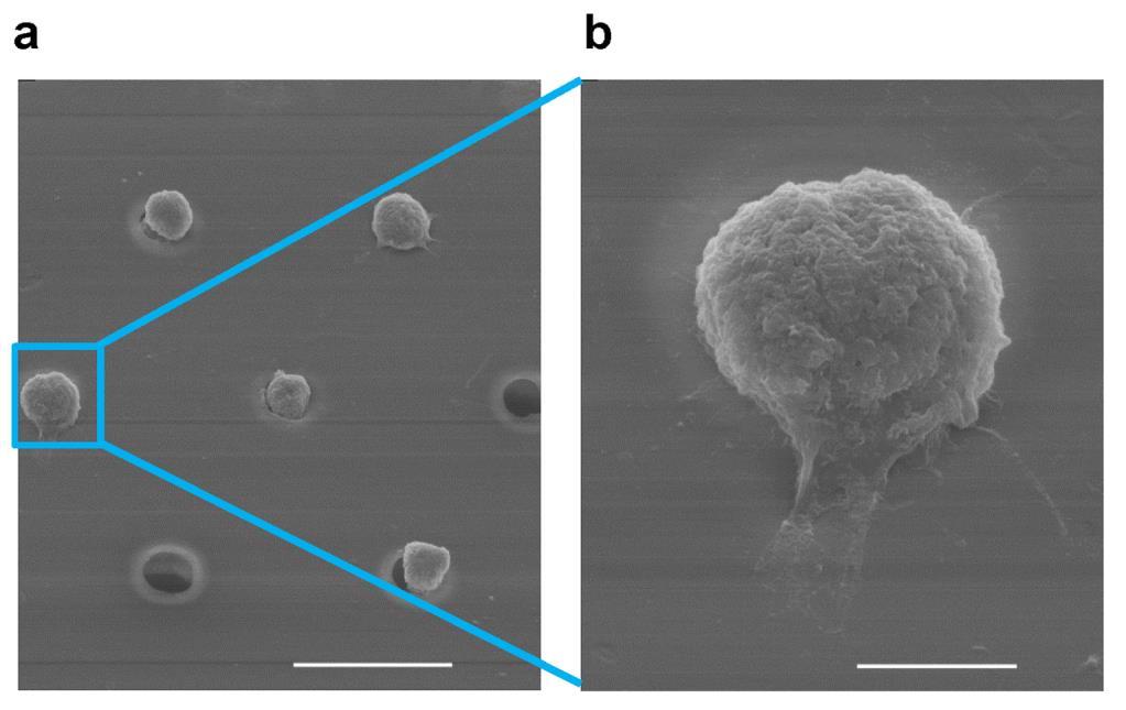
13 Supplementary Figure S6 13
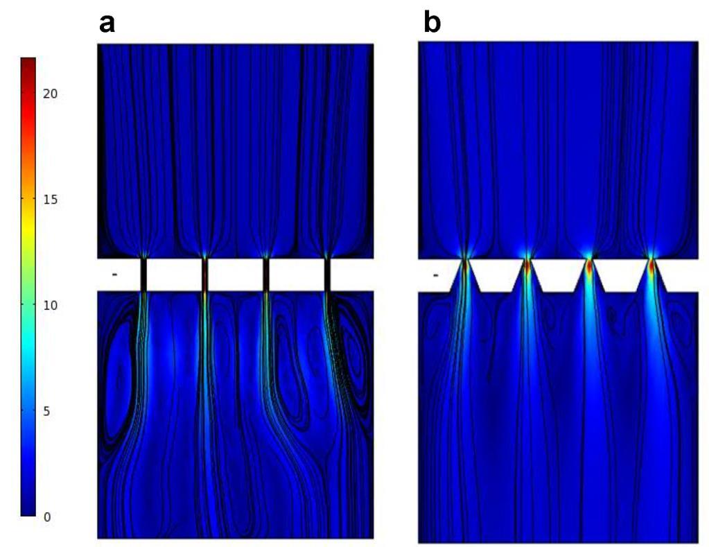
14 Supplementary Figure S7 14
Supplementary information
 Supplementary information Device Design The geometry of the microdevice channels were designed in autocad and modeled to simulate the microvasculature of the human body. In order to emulate physiologic
SUPPLEMENTAL INFORMATION: 1. Supplemental methods 2. Supplemental figure legends 3. Supplemental figures
 Supplementary Material (ESI) for Lab on a Chip This journal is The Royal Society of Chemistry 2008 A microfluidics-based turning assay reveals complex growth cone responses to integrated gradients of substrate-bound
Adhesion analysis of single circulating tumor cell on base layer of
 Electronic Supplementary Material (ESI) for Chemical Science. This journal is The Royal Society of Chemistry 2018 Supporting information Adhesion analysis of single circulating tumor cell on base layer
Leaf-inspired Artificial Microvascular Networks (LIAMN) for Threedimensional
 for Threedimensional") Electronic Supplementary Material (ESI) for RSC Advances. This journal is The Royal Society of Chemistry 2015 Supporting Information Leaf-inspired Artificial Microvascular Networks (LIAMN) for Threedimensional
Electronic Supplementary Material (ESI) for RSC Advances. This journal is The Royal Society of Chemistry 2015 Supporting Information Leaf-inspired Artificial Microvascular Networks (LIAMN) for Threedimensional
ELECTRONIC SUPPLEMENTARY INFORMATION Particle Sorting Using a Porous Membrane in a Microfluidic Device
 ELECTRONIC SUPPLEMENTARY INFORMATION Particle Sorting Using a Porous Membrane in a Microfluidic Device Huibin Wei, ab Bor-han Chueh, b Huiling Wu, bc Eric W. Hall, b Cheuk-wing Li, b Romana Schirhagl,
Large-scale fabrication of free-standing and sub-μm PDMS through-holes membranes
 Electronic Supplementary Material (ESI) for. This journal is The Royal Society of Chemistry 2018 Large-scale fabrication of free-standing and sub-μm PDMS through-holes membranes Hai Le-The,* a Martijn
Low-temperature, Simple and Fast Integration Technique of Microfluidic Chips by using a UV-curable Adhesive
 Low-temperature, Simple and Fast Integration Technique of Microfluidic Chips by using a UV-curable Adhesive Supplementary Information Channel fabrication Glass microchannels. A borosilicate glass wafer
Supporting Information
 Supporting Information The adhesion circle: A new approach to better characterize directional gecko-inspired dry adhesives Yue Wang, Samuel Lehmann, Jinyou Shao and Dan Sameoto* Department of Mechanical
Wang Chu Chien-Wen Research Presentation. By: Tae-Hyung Kang September 6th, 2013
 Wang Chu Chien-Wen Research Presentation By: Tae-Hyung Kang September 6th, 2013 Outline Introduction/Goal Fabrication/Mechanism Proposed Ideas/Approach Results Future Works Introduction Osmotic Valve:
Fabrication of Oxygenation Microfluidic Devices for Cell Cultures
 Fabrication of Oxygenation Microfluidic Devices for Cell Cultures Shauharda Khadka Department of Engineering Physics, Ramapo College of New Jersey, Mahwah, NJ Gerardo Mauleon and David T. Eddington Department
Fabrication of Oxygenation Microfluidic Devices for Cell Cultures
 1 Fabrication of Oxygenation Microfluidic Devices for Cell Cultures Shauharda Khadka skhadka@ramapo.edu Department of Engineering Physics, Ramapo College of New Jersey Gerardo Mauleon mauleon2@uic.edu
High-Throughput Single-Cell Derived Sphere Formation for Cancer Stem-Like Cell Identification and Analysis
 High-Throughput Single-Cell Derived Sphere Formation for Cancer Stem-Like Cell Identification and Analysis Yu-Chih Chen 1,3*, Patrick N. Ingram 2*, Shamileh Fouladdel 3, Sean P. McDermott 3, Ebrahim Azizi
Supporting Information. Monitoring Tumor Response to Anticancer Drugs. Using Stable Three-Dimensional Culture in a. Recyclable Microfluidic Platform
 Supporting Information Monitoring Tumor Response to Anticancer Drugs Using Stable Three-Dimensional Culture in a Recyclable Microfluidic Platform Wenming Liu,*,, Juan Xu, Tianbao Li, Lei Zhao, Chao Ma,
Fully-integrated, Bezel-less Transistor Arrays Using Reversibly Foldable Interconnects and Stretchable Origami Substrates
 Electronic Supplementary Material (ESI) for Nanoscale. This journal is The Royal Society of Chemistry 2016 Fully-integrated, Bezel-less Transistor Arrays Using Reversibly Foldable Interconnects and Stretchable
High-throughput Immunoassay through In-channel Microfluidic Patterning
 Supporting Information High-throughput Immunoassay through In-channel Microfluidic Patterning Chunhong Zheng, a,b Jingwen Wang, a Yuhong Pang, a,b Jianbin Wang, a Wenbin Li, c Zigang Ge,*,a and Yanyi Huang*,a,b
Supporting information for: Microfluidic single cell mrna isolation and analysis
 Supporting information for: Microfluidic single cell mrna isolation and analysis Joshua S. Marcus 1,2, W. French Anderson 2,3 & Stephen R. Quake 2,4,5 1 Biochemistry and Molecular Biophysics, 2 Applied
Supporting Information: Model Based Design of a Microfluidic. Mixer Driven by Induced Charge Electroosmosis
 Supporting Information: Model Based Design of a Microfluidic Mixer Driven by Induced Charge Electroosmosis Cindy K. Harnett, Yehya M. Senousy, Katherine A. Dunphy-Guzman #, Jeremy Templeton * and Michael
MICROFLUIDIC ASSEMBLY BLOCKS
 ELECTRONIC SUPPLEMENTARY INFORMATION MICROFLUIDIC ASSEMBLY BLOCKS Minsoung Rhee 1,2 and Mark A. Burns 1,3, * 1 Department of Chemical Engineering, the University of Michigan 2300 Hayward St. 3074 H.H.
Thermal Nanoimprinting Basics
 Thermal Nanoimprinting Basics Nanoimprinting is a way to replicate nanoscale features on one surface into another, like stamping copies are made by traditional fabrication techniques (optical/ebeam lith)
Supporting Information. Fabrication of Flexible Transparent Electrode with Enhanced Conductivity from Hierarchical Metal Grids
 Supporting Information Fabrication of Flexible Transparent Electrode with Enhanced Conductivity from Hierarchical Metal Grids Linjie Li, 1 Bo Zhang, 1 Binghua Zou, 1 Ruijie Xie, 1 Tao Zhang, 1 Sheng Li,
Alternative MicroFabrication and Applications in Medicine and Biology
 Alternative MicroFabrication and Applications in Medicine and Biology Massachusetts Institute of Technology 6.152 - Lecture 15 Fall 2003 These slides prepared by Dr. Hang Lu Outline of Today s Materials
Wireless implantable chip with integrated Nitinol-based pump for radio-controlled local drug delivery
 Electronic Supplementary Material (ESI) for Lab on a Chip. This journal is The Royal Society of Chemistry 2014 Electronic Supplementary Information Wireless implantable chip with integrated Nitinol-based
Figure SI-1. Fabrication process of the microchip. (A) Heater and sensor. 1) Au/Cr
 Heater and sensor. 1) Au/Cr") Electronic Supplementary Material (ESI) for RSC Advances. This journal is The Royal Society of Chemistry 2014 Supplemental Information 1. Microfluidic Device Fabrication Figure SI-1. Fabrication process
Electronic Supplementary Material (ESI) for RSC Advances. This journal is The Royal Society of Chemistry 2014 Supplemental Information 1. Microfluidic Device Fabrication Figure SI-1. Fabrication process
Supporting Information for. Co-Fabrication of Electromagnets and Microfluidic Systems. in Poly(dimethylsiloxane)
") Supporting Information for Co-Fabrication of Electromagnets and Microfluidic Systems in Poly(dimethylsiloxane) Adam C. Siegel, Sergey Shevkoplyas, Douglas B. Weibel, Derek Bruzewicz, Andres Martinez, and
Supporting Information for Co-Fabrication of Electromagnets and Microfluidic Systems in Poly(dimethylsiloxane) Adam C. Siegel, Sergey Shevkoplyas, Douglas B. Weibel, Derek Bruzewicz, Andres Martinez, and
Ostemer 322 Crystal Clear
 Ostemer 322 Crystal Clear Overview Name Description Recommended applications (see ostemers.com for references) Storage Handling Ostemer 322 Crystal Clear A dual cure polymer (UV + heat) with high transparency
Microfluidic for Testing Mechanical Properties of Cancer Cells
 Kaleidoscope Volume 11 Article 82 July 2014 Microfluidic for Testing Mechanical Properties of Cancer Cells Adrianne Shearer Follow this and additional works at: https://uknowledge.uky.edu/kaleidoscope
Supporting Information
 Electronic Supplementary Material (ESI) for Journal of Materials Chemistry C. This journal is The Royal Society of Chemistry 2018 Supporting Information Facile and highly efficient fabrication of robust
A new method to fabricate micro-structured products by. using a PMMA mold made by X-ray lithography
 A new method to fabricate micro-structured products by using a PMMA mold made by X-ray lithography Hiroyuki Ikeda SR center, Ritsumeikan University, 1-1-1 Noji-Higashi, Kusatsu 525-8577, Japan Abstract
µ Slide Membrane ibipore Flow
 The ibidi product family is comprised of a variety of µ Slides and µ Dishes, which have all been designed for high end microscopic analysis of fixed or living cells. The high optical quality of the material
Applications of Nano Patterning Process 1. Patterned Media
 Applications of Nano Patterning Process 1. Patterned Media Contents Introduction Part. 1. Nanoimprinting on Glass Substrate for Patterned Media Part. 2. Nanoinjection Molding of Nanopillars for Patterned
Module 13: Soft Lithography. Lecture 19: Soft Lithography 2
 Module 13: Soft Lithography Lecture 19: Soft Lithography 2 1 In the previous lecture we have introduced the concept of Soft Lithography and discussed three of the methods, which are Replica Molding, Micro
Supporting Information
 Ice-Binding Proteins that Accumulate on Different Ice Crystal Planes Produces Distinct Thermal Hysteresis Dynamics Ran Drori 1, Yeliz Celik 2, Peter L. Davies 3 and Ido Braslavsky 1,2 1 Institute of Biochemistry,
SEPARATING PLASMA AND BLOOD CELLS BY DIELECTROPHORESIS IN MICROFLUIDIC CHIPS
 Fourth International Symposium on Physics of Fluids (ISPF4) International Journal of Modern Physics: Conference Series Vol. 19 (2012) 185 189 World Scientific Publishing Company DOI: 10.1142/S2010194512008732
Fabricating Microfluidic Devices for High-Density Biological Assays
 Fabricating Microfluidic Devices for High-Density Biological Assays Todd Thorsen Department of Mechanical Engineeering MIT Panamerican Advanced Studies Institute Micro-Electro-Mechanical Systems San Carlos
OPTICAL CONTROL OF TUMOR INDUCTION IN THE ZEBRAFISH
 OPTICAL CONTROL OF TUMOR INDUCTION IN THE ZEBRAFISH Zhiping Feng, 1,12 Suzy Nam, 2 Fatima Hamouri, 3,4 Isabelle Aujard, 5,6 Bertrand Ducos, 3,4 Sophie Vriz, 7,8 Michel Volovitch, 7,9 Ludovic Jullien, 5,6
UV15: For Fabrication of Polymer Optical Waveguides
 CASE STUDY UV15: For Fabrication of Polymer Optical Waveguides Master Bond Inc. 154 Hobart Street, Hackensack, NJ 07601 USA Phone +1.201.343.8983 Fax +1.201.343.2132 main@masterbond.com CASE STUDY UV15:
Superamphiphobic Silicon Nanowires Embedded Microsystem. and In-Contact Flow Performance of Gas and Liquid Streams
 Supporting Information Superamphiphobic Silicon Nanowires Embedded Microsystem and In-Contact Flow Performance of Gas and Liquid Streams Dong-Hyeon Ko, a Wurong Ren, b Jin-Oh Kim, a Jun Wang, b Hao Wang,
Microcontact Printing Procedures for Adhesive and Conductive Epoxies
 Microcontact Printing Procedures for Adhesive and Conductive Epoxies This objective was accomplished through a formal record of the procedures to deliver a stamped product which met the benchmark mechanical,
Soft Lithography. Jin-Goo Park. Materials and Chemical Engineering Hanyang University, Ansan. Electronic Materials and Processing Lab.
 Hanyang University Soft Lithography Jin-Goo Park Materials and Chemical Engineering Hanyang University, Ansan Electronic Materials and Processing Lab. Introduction to Soft Lithography Research Micro- Electro-
µ Slide Membrane ibipore Flow
 The ibidi product family is comprised of a variety of µ Slides and µ Dishes, which have all been designed for high end microscopic analysis of fixed or living cells. The high optical quality of the material
Nanoscale Plasmonic Interferometers for Multi-Spectral, High-Throughput Biochemical Sensing
 Supporting Online Information for Nanoscale Plasmonic Interferometers for Multi-Spectral, High-Throughput Biochemical Sensing Jing Feng (a), Vince S. Siu (a), Alec Roelke, Vihang Mehta, Steve Y. Rhieu,
Flow-Through Electroporation in Asymmetric Curving Microfluidic Channels
 Flow-Through Electroporation in Asymmetric Curving Microfluidic Channels Hamid Hassanisaber Thesis submitted to the faculty of the Virginia Polytechnic Institute and State University in partial fulfillment
Methods of manufacture
 1 Methods of manufacture For Ceramics (see (b)) Crush raw materials Shape the crushed raw materials (various means) Dry & fire Apply finishing operations, as needed; to achieve required dimensional tolerances
Cost Effective 3D Glass Microfabrication for Advanced Packaging Applications
 Cost Effective 3D Glass Microfabrication for Advanced Packaging Applications Authors: Jeb. H Flemming, Kevin Dunn, James Gouker, Carrie Schmidt, Roger Cook ABSTRACT Historically, while glasses have many
High-Throughput Method for Microfluidic Placement of Cells in Micropatterned Tissues
 High-Throughput Method for Microfluidic Placement of Cells in Micropatterned Tissues Emily N. Sevcik Faculty Mentor: Patrick W. Alford Undergraduate Research Opportunities Program Project Final Report
Polymer-based Microfabrication
 Polymer-based Microfabrication PDMS SU-8 PMMA Hydrogel 1 Soft Lithography Developed by Whitesides, et. al A set of techniques for microfabrication based on the use of lithography, soft substrate materials
Outline. Introduction to the LIGA Microfabrication Process. What is LIGA? The LIGA Process. Dr. Bruce K. Gale Fundamentals of Microfabrication
 Outline Introduction to the LIGA Microfabrication Process Dr. Bruce K. Gale Fundamentals of Microfabrication What is LIGA? The LIGA Process Lithography Techniques Electroforming Mold Fabrication Analyzing
Journal of Advanced Mechanical Design, Systems, and Manufacturing
 Fabrication of the X-Ray Mask using the Silicon Dry Etching * Hiroshi TSUJII**, Kazuma SHIMADA**, Makoto TANAKA**, Wataru YASHIRO***, Daiji NODA** and Tadashi HATTORI** **Laboratory of Advanced Science
Membrane-less microfiltration using inertial microfluidics
 Membraneless microfiltration using inertial microfluidics Majid Ebrahimi Warkiani, Andy Tay, Guofeng Guan, and Jongyoon Han Supplementary information Table S1. Head to head comparison of inertial filtration
Supplementary Information. for
 Electronic Supplementary Material (ESI) for ChemComm. This journal is The Royal Society of Chemistry 2014 Supplementary Information for Nanoslitting Phase-separated Block Copolymers by Solvent Swelling
Application Microfluidic Cell Analysis Devices (I) Date: 2013/05/24. Dr. Yi-Chung Tung
 Date: 2013/05/24. Dr. Yi-Chung Tung") Application Microfluidic Cell Analysis Devices (I) Date: 2013/05/24 Dr. Yi-Chung Tung Mechanotransduction and the Study of Cellular Forces Mechanical forces play a critical role in nearly all aspects of
Application Microfluidic Cell Analysis Devices (I) Date: 2013/05/24 Dr. Yi-Chung Tung Mechanotransduction and the Study of Cellular Forces Mechanical forces play a critical role in nearly all aspects of
Part HD head control arm
 Part HD head control arm Quality characteristics Dimension: height, width, wall thickness Mechanical properties of materials: hardness, brittleness, and porosity. Machining Dimension: holes, grooves, and
FABRICATION OF MICROFLUIDIC CHANNELS USING MICROFIBERS FOR APPLICATIONS IN BIOTECHNOLOGY
 FABRICATION OF MICROFLUIDIC CHANNELS USING MICROFIBERS FOR APPLICATIONS IN BIOTECHNOLOGY Tom Huang, 1,5 Woo-Jin Chang, 2 Demir Akin, 2 Rafael Gomez, 2 Rashid Bashir, 2,3 Nathan Mosier, 4 and Michael R.
Micro Injection Molding of Micro Fluidic Platform
 Micro Injection Molding of Micro Fluidic Platform S. C. Chen, J. A. Chang, Y. J. Chang and S. W. Chau Department of Mechanical Engineering, Chung Yuan University, Taiwan, ROC Abstract In this study, micro
Single-digit-resolution nanopatterning with. extreme ultraviolet light for the 2.5 nm. technology node and beyond
 Electronic Supplementary Material (ESI) for Nanoscale. This journal is The Royal Society of Chemistry 205 Supplementary Information for: Single-digit-resolution nanopatterning with extreme ultraviolet
2300 Hayward St H.H. Dow Building, Ann Arbor, MI Palmer Commons, 100 Washtenaw Avenue, Ann Arbor, MI
 MICROFLUIDIC ASSEMBLY BLOCKS Minsoung Rhee 1,2 and Mark A. Burns 1,3, * 1 Department of Chemical Engineering, the University of Michigan 2300 Hayward St. 3074 H.H. Dow Building, Ann Arbor, MI 48109-2136
GLM General information. Technical Datasheet
 GLM 2060 Nanocomposite SU-8-negative tone photo-epoxy for layers from 6.0 to 50µm Technical Datasheet Gersteltec Sarl. Générale Guisan 26, 1009, Pully Switzerland Switzerland / Israel / Taiwan Contact:
Photo-Patternable and Adhesive Polymer for Wafer-Scale Microfluidic Device Fabrication
 Photo-Patternable and Adhesive Polymer for Wafer-Scale Microfluidic Device Fabrication Sara Peeters Bivragh Majeed Josine Loo Katsuhiko Hieda Tom Miyazaki Chengxun Liu John O Callaghan Karolien Jans Liesbet
FABRICATION OF CERAMIC COMPONENTS FOR MICRO GAS TURBINE ENGINES
 FABRICATION OF CERAMIC COMPONENTS FOR MICRO GAS TURBINE ENGINES H.-C. Liu, S. Kang, F.B. Prinz J. Stampfl Rapid Prototyping Laboratory TU Wien Building 530 Room 226 Inst. für Werkstoffkunde und Materialpruefung
Simple UV-based Soft-lithography Process for. Fabrication of Low-Loss Polymer PSQ-L-based. Waveguides
 Simple UV-based Soft-lithography Process for Fabrication of Low-Loss Polymer PSQ-L-based Waveguides Jie Teng 1, 2, 4, Stijn Scheerlinck 4, Geert Morthier 4, Roel Baets 4, Hongbo Zhang 2,3, Xigao Jian 2,3,
Supporting Information
 Copyright WILEY-VCH Verlag GmbH & Co. KGaA, 69469 Weinheim, Germany, 2013. Supporting Information for Adv. Mater., DOI: 10.1002/adma.201300794 Highly Stretchable Patterned Gold Electrodes Made of Au Nanosheets
Introduction to Micro/Nano Fabrication Techniques. Date: 2015/05/22 Dr. Yi-Chung Tung. Fabrication of Nanomaterials
 Introduction to Micro/Nano Fabrication Techniques Date: 2015/05/22 Dr. Yi-Chung Tung Fabrication of Nanomaterials Top-Down Approach Begin with bulk materials that are reduced into nanoscale materials Ex:
Supplementary Information
 Electronic Supplementary Material (ESI) for Nanoscale. This journal is The Royal Society of Chemistry 2017 Supplementary Information Spatially Controlled Positioning of Coordination Polymer Nanoparticles
Microfluidic Systems for Cell Growth and Cell Migration Studies
 Microfluidic Systems for Cell Growth and Cell Migration Studies Maria Dimaki 1, Pranjul Shah 1, Dorota Kwasny 1, Jacob Moresco 2 and Winnie E. Svendsen 1 1 DTU Nanotech Department of Micro- and Nanotechnology,
The Effect of Hydrophobic Patterning on Micromolding of Aqueous-Derived Silk Structures
 The Effect of Hydrophobic Patterning on Micromolding of Aqueous-Derived Silk Structures Konstantinos Tsioris 1, Robert D White 1, David L Kaplan 2, and Peter Y Wong 1 1 Mechanical Engineering, Tufts University,
Automation of Cellular Sample Preparation Using a Centrifuge-on-a-Chip
 Automation of Cellular Sample Preparation Using a Centrifuge-on-a-Chip Albert J. Mach, Jae Hyun Kim, Armin Arshi, Soojung Claire Hur and Dino Di Carlo Supplementary figures and text: Supplementary Figure
High Sensitivity of Phase-based Surface Plasmon Resonance in Nano-cylinder Array
 PIERS ONLINE, VOL. 4, NO. 7, 2008 746 High Sensitivity of Phase-based Surface Plasmon Resonance in Nano-cylinder Array Bing-Hung Chen, Yih-Chau Wang, and Jia-Hung Lin Institute of Electronic Engineering,
Single-Cell Electroporation Using a Multifunctional Pipette
 Single-Cell Electroporation Using a Multifunctional Pipette Alar Ainla, Shijun Xu, Nicolas Sanchez, Gavin D. M. Jeffries and Aldo Jesorka Electronic Supplementary Information (ESI) Table of contents Table
NanoSystemsEngineering: NanoNose Final Status, March 2011
 1 NanoSystemsEngineering: NanoNose Final Status, March 2011 The Nanonose project is based on four research projects (VCSELs, 3D nanolithography, coatings and system integration). Below, the major achievements
Supplementary Information for. Fast Analysis of Intracellular Glucose at Single Cells using Electrochemiluminescence Imaging
 Supplementary Information for Fast Analysis of Intracellular Glucose at Single Cells using Electrochemiluminescence Imaging Jingjing Xu, Peiyuan Huang, Yu Qin, Dechen Jiang*, Hong-yuan Chen State Key Laboratory
Supporting information
 Supporting information In situ purification to eliminate the influence of impurities in solution-processed organic crystals for transistor arrays Yun Li, a,b,* Chuan Liu, a,* Micael V. Lee, a Yong Xu,
ELECTRONIC SUPPLEMENTARY INFORMATION. On-Skin Liquid Metal Inertial Sensor
 Electronic Supplementary Material (ESI) for Lab on a Chip. This journal is The Royal Society of Chemistry 2017 ELECTRONIC SUPPLEMENTARY INFORMATION On-Skin Liquid Metal Inertial Sensor Matija Varga, a,b
EXPLORING VACUUM CASTING TECHNIQUES FOR MICRON AND SUBMICRON FEATURES. Campus Ker Lann, av Robert Schumann Bruz, France
 EXPLORING VACUUM CASTING TECHNIQUES FOR MICRON AND SUBMICRON FEATURES M. Denoual *, P. Mognol **, B. Lepioufle * * Biomis-SATIE ENS-Cachan antenne de Bretagne, Campus Ker Lann, av Robert Schumann 35170
INTRODUCTION Intrinsic cellular mechanical properties (e.g., instantaneous Young s modulus (E instantaneous ) and
 and") TUMOR CELL CLASSIFICATION BASED ON INSTANTANEOUS YOUNG S MODULUS USING CONSTRICTION CHANNEL BASED MICROFLUIDIC DEVICES Y. Luo 1, D. Chen 1, Y. Zhao 1, C. Wei 1, X. Zhao 2, W. Yue 2, R. Long 3*, J. Wang
TUMOR CELL CLASSIFICATION BASED ON INSTANTANEOUS YOUNG S MODULUS USING CONSTRICTION CHANNEL BASED MICROFLUIDIC DEVICES Y. Luo 1, D. Chen 1, Y. Zhao 1, C. Wei 1, X. Zhao 2, W. Yue 2, R. Long 3*, J. Wang
Precision etching of micro components
 Precision etching of micro components A High-Tech Profile Micrometal manufactures customized, highly accurate etched components. We photochemically etch these parts from thin materials (starting at 0.025
SUPPLEMENTARY INFORMATION
 Large-area, flexible 3D optical negative index metamaterial formed by nanotransfer printing DebashisChanda 1, KazukiShigeta 1, Sidhartha Gupta 1, Tyler Cain 1, Andrew Carlson 1, Agustin Mihi 1, Alfred
Fabrication of Microchannel and Micro Chamber for Microfluidic Lab-on-Chip
 Australian Journal of Basic and Applied Sciences, 7(1): 166-170, 2013 ISSN 1991-8178 Fabrication of Microchannel and Micro Chamber for Microfluidic Lab-on-Chip 1 U. Hashim, 1 Tijjani Adam and 2 Peter Ling
Precision etching of micro components
 Precision etching of micro components A High-Tech Profile Micrometal manufactures customized, highly accurate etched components. We photochemically etch these parts from thin materials (starting at 0.025
High-throughput analysis of single hematopoietic stem cell proliferation in microfluidic cell culture arrays
 Nature Methods High-throughput analysis of single hematopoietic stem cell proliferation in microfluidic cell culture arrays Véronique Lecault, Michael VanInsberghe, Sanja Sekulovic, David J H F Knapp,
Micro-Nano Fabrication Research
 Micro-Nano Fabrication Research Technical Education Quality Improvement Programme 22-23 December 2014 Dr. Rakesh G. Mote Assistant Professor Department of Mechanical Engineering IIT Bombay rakesh.mote@iitb.ac.in;
Phagocytosis Assay Kit (IgG PE)
") Phagocytosis Assay Kit (IgG PE) Item No. 600540 www.caymanchem.com Customer Service 800.364.9897 Technical Support 888.526.5351 1180 E. Ellsworth Rd Ann Arbor, MI USA TABLE OF CONTENTS GENERAL INFORMATION
Phagocytosis Assay Kit (IgG PE) Item No. 600540 www.caymanchem.com Customer Service 800.364.9897 Technical Support 888.526.5351 1180 E. Ellsworth Rd Ann Arbor, MI USA TABLE OF CONTENTS GENERAL INFORMATION
Process considerations to achieve optimum weld strengths of Wood Plastics Composites using advanced Vibration Welding technology
 Process considerations to achieve optimum weld strengths of Wood Plastics Composites using advanced Vibration Welding technology Michael J. Johnston, Dukane Corporation As the uses for Wood Plastic Composites
Immunofluorescence Staining Protocol for 3 Well Chamber, removable
 Immunofluorescence Staining Protocol for 3 Well Chamber, removable This Application Note presents a simple protocol for the cultivation, fixation, and staining of cells using the 3 Well Chamber, removable.
A microfluidic cell culture device with integrated microelectrodes for barrier studies.
 Downloaded from orbit.dtu.dk on: Dec 30, 2018 A microfluidic cell culture device with integrated microelectrodes for barrier studies. Tan, Hsih-Yin; Dufva, Martin; Kutter, Jörg P.; Andresen, Thomas Lars
Chapter 4 Fabrication Process of Silicon Carrier and. Gold-Gold Thermocompression Bonding
 Chapter 4 Fabrication Process of Silicon Carrier and Gold-Gold Thermocompression Bonding 4.1 Introduction As mentioned in chapter 2, the MEMs carrier is designed to integrate the micro-machined inductor
YIELD IMPROVEMENT CASE STUDY: STACKED SPRING CAPS
 YIELD IMPROVEMENT CASE STUDY: STACKED SPRING CAPS Shouzhu Ou 1, Kent Carlson 1, Malcolm Blair 2, Graham Jones 3, Richard Hardin 1 and Christoph Beckermann 4 1 Research Engineers, Department of Mechanical
Artificial Alveolar-Capillary Membrane on a Microchip
 Artificial Alveolar-Capillary Membrane on a Microchip Keith Male Advisor: Dr. Richard Savage Materials Engineering Department California Polytechnic State University San Luis Obispo, California June 1,
Influence of Electric Fields and Conductivity on Pollen Tube Growth assessed via Electrical Lab-on-Chip
 SUPPLEMENTAL MATERIAL Influence of Electric Fields and Conductivity on Pollen Tube Growth assessed via Electrical Lab-on-Chip Carlos Agudelo 1, Muthukumaran Packirisamy 1, Anja Geitmann 2* 1 Optical Bio-Microsystem
FABRICATION FOR MICRO PATTERNS OF NICKEL MATRIX DIAMOND COMPOSITES USING THE COMPOSITE ELECTROFORMING AND UV- LITHOGRAPHY
 16 TH INTERNATIONAL CONFERENCE ON COMPOSITE MATERIALS FABRICATION FOR MICRO PATTERNS OF NICKEL MATRIX DIAMOND COMPOSITES USING THE COMPOSITE ELECTROFORMING AND UV- LITHOGRAPHY Tsung-Han Yu, Shenq-Yih Luo,
Highly transparent and flexible circuits through patterning silver nanowires into
 Electronic Supplementary Material (ESI) for ChemComm. This journal is The Royal Society of Chemistry 2018 Highly transparent and flexible circuits through patterning silver nanowires into microfluidic
Table of Contents. Robert A. Malloy. Plastic Part Design for Injection Molding. An Introduction ISBN:
 Table of Contents Robert A. Malloy Plastic Part Design for Injection Molding An Introduction ISBN: 978-3-446-40468-7 For further information and order see http://www.hanser.de/978-3-446-40468-7 or contact
Electronic Supplementary Information
 Electronic Supplementary Information Fabrication of nickel molds. A Graphtec Craft Robo Pro CE5000-40 Cutting Plotter (Graphtec America, Inc.) was used to plot CAD designs directly from a.dwg or.dxf file
Holography of Making 1D-Nano-Trench-Lines and 2D-Nano-Posts
 Laser: He-Cd Gas Laser ( =325nm). Pitch Distance d: 200~300nm ( : 54~33 o ). Holography of Making 1D-Nano-Trench-Lines and 2D-Nano-Posts A)Process Details of the holographic 1D-line pattern (210nm thick
In operandi observation of dynamic annealing: a case. Supplementary Material
 In operandi observation of dynamic annealing: a case study of boron in germanium nanowire devices Supplementary Material Maria M. Koleśnik-Gray, 1,3,4 Christian Sorger, 1 Subhajit Biswas, 2,3 Justin D.
Precision etching of micro components
 Precision etching of micro components A High-Tech Profile Micrometal manufactures customized, highly accurate etched components. We photochemically etch these parts from thin materials (starting at 0.025
Supporting Information
 Supporting Information In situ Active Poling of Nanofibers Network for Gigantically Enhanced Particulate Filtration Chun Xiao Li,, Shuang Yang Kuang,, Yang Hui Chen,, Zhong Lin Wang,,,#, Congju Li, and
Micro and nano structuring of carbon based materials for micro injection moulding and hot embossing
 Micro and nano structuring of carbon based materials for micro injection moulding and hot embossing Victor Usov, Graham Cross, Neal O Hara, Declan Scanlan, Sander Paulen, Chris de Ruijter, Daniel Vlasveld,
Supporting Information. graphene oxide films for detection of low. concentration biomarkers in plasma
 Supporting Information Wafer-scale high-resolution patterning of reduced graphene oxide films for detection of low concentration biomarkers in plasma Jinsik Kim a, Myung-Sic Chae a, Sung Min Lee b, Dahye
Stork Veco. Shaping the future with Electrofoming. Metal precision
 Metal precision Electroforming: A technology you should know more about! Content: Company profile Google results on Electroforming. Advantages of Electroforming Explanation of the process. Galvanic coatings.
Supporting Information: Gold nanorod plasmonic upconversion microlaser
 Supporting Information: Gold nanorod plasmonic upconversion microlaser 1 Materials Synthesis and Properties Ce Shi, Soheil Soltani, Andrea M. Armani 1.1 Nanorod synthesis First the gold nanorods (NRs)