High Resolution Neuro-Electronic Interface System for Electrophysiological Experiments
|
|
|
- Preston Page
- 6 years ago
- Views:
Transcription
1 High Resolution Neuro-Electronic Interface System for Electrophysiological Experiments Research presentation by Neil Joye (LSM, EPFL) on the 20 th June 2007
2 Content Introduction State of the Art 3D tip electrodes Current work MEA manufacturing Modeling Packaging Future work CMOS design and CMOS postprocessing
3 Introduction Goal of the work Built very high-density Microelectrode Arrays (MEAs) with CMOS processing on chip for recording and stimulating electrical activity in neuron cultures. In collaboration with the Laboratory of Neural Microcircuitry (LNMC) of the Brain Mind Institute MEA Neuron Neuron Culture Sensors / Actuators PC CMOS circuit Processing (Amplification, Addressing, ADC, )
4 Introduction Extracellular voltage that is sensed is 3-4 orders of magnitude smaller than the intracellular voltage (action potential) Main challenge High spatial resolution Small electrode size High electrode impedance High SNR
5 State of the Art (1) Prof. Hierlemann s group (ETHZ) 1 8 x 16 = 128 electrodes Techno CMOS 0.6 µm Sensor diameter = µm Pitch = µm Input noise = 17 µvrms (with 20 µm diameter electrodes) Advantages Able to record and stimulate A lot of signal processing is already done at the pixel level Low noise Disadvantages Low spatial resolution (neuron size around 10 µm) 1 F. Heer et al., Biosensors and Bioelectronics, 2007
6 State of the Art (1) F. Heer et al., JSSC, 2006 F. Heer et al., Biosensors and Bioelectronics, 2007
7 State of the Art (1) D.A Wagenaar et al., Journal of Neuroscience, 2005
8 State of the Art (1) F. Heer et al., Biosensors and Bioelectronics, 2007
9 State of the Art (1) F. Heer et al., Biosensors and Bioelectronics, 2007
10 State of the Art (2) SAMLAB, IMT, University of Neuchatel 2 64 x 64 = electrodes Techno CMOS 0.5 µm Sensor size = 20 x 20 µm 2 Pitch = 40 µm Input noise = 80 µvrms Advantages Higher spatial resolution (only 8 transistors per pixel) Disadvantages Higher input noise 2 L. Berdondini et al., Biosensors and Bioelectronics, 2005

11 State of the Art (2) L. Berdondini et al., Biosensors and Bioelectronics, 2005

12 3D tip electrodes Goal Decrease the distance electrode-neuron in order to improve the neuron-electrode coupling This assumption is currently being tested and proved theoretically with an electrical model experimentally with electrophysiological measurements
13 Current work A first generation of MEA is being manufactured at the moment in CMI No CMOS processing is done on these chips (future work) 3 versions are planed to be manufactured MEA Neuron Neuron Culture Sensors / Actuators PC CMOS circuit Processing (Amplification, Addressing, ADC, )
 Improve the neuron-sensor model that is being")
14 MEA version-1 Planar electrodes 6 x 6 = 64 electrodes Sensor size 2 20 µm Pixel size 4 40 µm Goal Compare measurements with different sensor and pixel sizes Results will be compared with the one obtained from 3D tip electrodes (version-2) Improve the neuron-sensor model that is being developed

15 MEA version-1
 Measure electrical and biological characteristics of these arrays Establish a controlled and straightforward manufacturing process for these 3D tip electrode")
16 MEA version-2 3D tip electrodes Output wiring done on the surface Goal Study the manufacturing of the 3D tip electrodes (size, shape, process characteristics, etc.) Measure electrical and biological characteristics of these arrays Establish a controlled and straightforward manufacturing process for these 3D tip electrode arrays

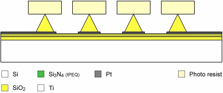
17 MEA version-2

18 MEA version-2

19 MEA version-2
20 MEA version-2 Challenges We are approaching the size limit for the 3D tip electrodes manufacturing

21 MEA version-3 3D tip electrode arrays with output wiring on 2 metal layers Biological measurements Compare with planar electrodes Compare with simulations obtained using developed model Improvement of the model to be made if necessary
22 Neuron-Sensor Model (1) Based on Hodgkin-Huxley model A model of the interaction between neurons and planar electrodes is being developed Simulations will be compared with biological and electrical measurements in order to improve the model I. Schoen and P. Fromherz, Biophysical Journal, 2007
23 Neuron-Sensor Model (2) For the 3D tip electrodes, a lower level model is been developed Lower level Electrical field Our model will be used for electrodes which are one order of magnitude smaller than the one shown on this graph M.O. Heuschkel el al., Journal of Neuroscience Methods, 2002
24 Neuron-Sensor Model (2) Current work using FEMLAB simulations
 Planar electrode 3D tip")
25 Neuron-Sensor Model (2) Current flow from neuron to electrode (recording of an action potential) Planar electrode 3D tip electrode

26 Neuron-Sensor Model (2) Electrical field simulation

27 Neuron-Sensor Model (2) Voltage potential simulation
28 Neuron-Sensor Model (2) Current and future work Improving the model Using the reel action potential waveform instead of a constant voltage Simulating the current flow from electrode to neuron (stimulation of an action potential) Simulating the interaction between a neuron culture and an electrode array Final goal of the model Find the optimum electrode array Size, shape, pitch, etc.


29 Packaging PCB must be compatible with Multi Channel Systems equipment (used in LNMC) Packaging must protect the bond wires from being attacked by physiological solutions Bond wires must not be pulled off, either by thermal expansion of by swelling of the material due to liquid absorption In future work, alternatives to wire bonding will be investigated
30 Future work (CMOS) MEA Neuron Neuron Culture Sensors / Actuators PC CMOS circuit Processing (Amplification, Addressing, ADC, ) A CMOS chip is expected to be taped out during this fall Different functionalities will be implemented on this integrated circuit Amplification stage Filtering Addressing of each sensor Then, post-fabrication of electrodes on the surface of the chip is expected to be done next spring
A 256-by-256 CMOS Microelectrode Array for Extracellular Neural Stimulation of Acute Brain Slices. Columbia University, New York, NY
 A 256-by-256 CMOS Microelectrode Array for Extracellular Neural Stimulation of Acute Brain Slices Na Lei 1, K L Shepard 1, Brendon O Watson 2, Jason N MacLean 2, Rafael Yuste 2 1 Department of Electrical
Implantable Microelectronic Devices
 ECE 8803/4803 Implantable Microelectronic Devices Fall - 2015 Maysam Ghovanloo (mgh@gatech.edu) School of Electrical and Computer Engineering Georgia Institute of Technology 2015 Maysam Ghovanloo 1 Outline
Embedding of Active Components in LCP for Implantable Medical Devices
 44 th IMAPS New England Symposium 2017 Embedding of Active Components in LCP for Implantable Medical Devices Dr. Eckardt Bihler and Dr. Marc Hauer, Dyconex AG Susan Bagen, PE, Micro Systems Technologies,
Improving Neuron Stimulation Efficency by Altering Electrode Geometry
 Improving Neuron Stimulation Efficency by Altering Electrode Geometry A. Ghazavi 1, D. Westwick 1, C. Luk 2, N. I. Syed 2 and C. Dalton 1 1 Department of Electrical and Computer Engineering, University
Voltage clamp and patch-clamp techniques
 Voltage clamp and patch-clamp techniques Dr. Nilofar Khan Objectives Historical background Voltage Clamp Theory Variations of voltage clamp Patch-clamp Principal Patch-clamp configurations Applications
SILICON MICROSTRUCTURES FOR NEURO-ELECTRONICS APPLICATIONS
 SIICON MICROSTRUCTURES FOR NEURO-EECTRONICS APPICATIONS HENRIQUE E. M. PERES (1), NATHAIA. V. PEIXOTO (2), FRANCISCO J. R. FERNANDEZ (3) and WAGNER W. EITE Grupo de Sensores Integráveis e Microestruturas
An SOI Process for Fabrication. of Solar Cells, Transistors and Electrostatic Actuators. Berkeley Sensor and Actuator Center
 An SOI Process for Fabrication of Solar Cells, Transistors and Electrostatic Actuators Colby L Bellew, Seth Hollar and K.S.J. Pister University of California at Berkeley Berkeley Sensor and Actuator Center
Microelectronics. Integrated circuits. Introduction to the IC technology M.Rencz 11 September, Expected decrease in line width
 Microelectronics Introduction to the IC technology M.Rencz 11 September, 2002 9/16/02 1/37 Integrated circuits Development is controlled by the roadmaps. Self-fulfilling predictions for the tendencies
Micro and Nano technologies for Health sensors development (part.2)
") Micro and Nano technologies for Health sensors development (part.2) Nadia Madaoui (nadia.madaoui@esiee.fr) Lionel Rousseau : (lionel.rousseau@esiee.fr) Laurie Valbin : (laurie.valbin@esiee.fr) Olivier
Micro and Nano technologies for Health sensors development (part.2) Nadia Madaoui (nadia.madaoui@esiee.fr) Lionel Rousseau : (lionel.rousseau@esiee.fr) Laurie Valbin : (laurie.valbin@esiee.fr) Olivier
Methods of Characterizing Neural Networks
 Methods of Characterizing Neural Networks Ashley Nord University of Minnesota Minneapolis, MN 55414 Advisors: Katsushi Arisaka, Adrian Cheng University of California Los Angeles Los Angeles, CA 90024 September
Packaging Commercial CMOS Chips for Lab on a Chip Integration
 Supporting Information for Packaging Commercial CMOS Chips for Lab on a Chip Integration by Timir Datta-Chaudhuri, Pamela Abshire, and Elisabeth Smela Biocompatibility Although the supplier s instructions
Ionscope SICM. About Ionscope. Scanning Ion Conductance Microscopy. Ionscope A brand of OpenIOLabs Limited
 SICM About is a brand of OpenIOLabs Ltd, headquartered in Cambridge UK, is the worldleader in (SICM), a rapidly emerging Scanning Probe Microscopy (SPM) technique which allows nanoscale topographical mapping
Polymer Composite with Carbon Nanofibers. Aligned during Thermal Drawing as a. Microelectrode for Chronic Neural Interfaces
 Polymer Composite with Carbon Nanofibers Aligned during Thermal Drawing as a Microelectrode for Chronic Neural Interfaces Yuanyuan Guo 1,2*, Shan Jiang 2, Benjamin J.B. Grena 3, Ian F. Kimbrough 4, Emily
THE HOPFIELD AND KOHONEN NETWORKS: AN IN VIVO TEST
 THE HOPFIELD AND KOHONEN NETWORKS: AN IN VIVO TEST Rita Pizzi 1, Andrea Fantasia 1, Danilo Rossetti 1, Giovanni Cino 1, Fabrizio Gelain 2 and Angelo Vescovi 2 1 Department of Information Technologies,
Design, Simulation and Study of MEMS Based Micro-needles and Micro-pump for Biomedical Applications
 Design, Simulation and Study of MEMS Based Micro-needles and Micro-pump for Biomedical Applications Presented by Pranay Kanti Podder Dhiman Mallick Dip Prakash Samajdar Anirban Bhattacharyya Institute
UNIT I PHYSIOLOGYAND TRANSDUCERS
 SRI VENKATESWARA COLLEGE OF ENGINEERING AND TECHNOLOGY TIRUPACHUR DEPARTMENT OF ELECTRICAL AND ELECTRONICS ENGINEERING 1. What is meant by cell? EI 2311 BIOMEDICAL INSTRUMENTATION 2 Mark Questions With
Controlling life with photons A new tool based on conjugated polymers
 Controlling life with photons A new tool based on conjugated polymers Maria Rosa Antognazza Center for Nanoscience and Technology @PoliMi The Italian Institute of Technology Controlling life with photons:
New Technology for High-Density LSI Mounting in Consumer Products
 New Technology for High-Density Mounting in Consumer Products V Hidehiko Kira V Akira Takashima V Yukio Ozaki (Manuscript received May 29, 2006) The ongoing trend toward downsizing and the growing sophistication
Surface Micromachining of Uncooled Infrared Imaging Array Using Anisotropic Conductive Film
 Surface Micromachining of Uncooled Infrared Imaging Array Using Anisotropic Conductive Film Weiguo Liu, Lingling Sun, Weiguang Zhu, Ooi Kiang Tan Microelectronics Center, School of Electrical and Electronic
Chamber Temperature Measurement of Micro PCR Chip Using Thermocouple
 Chamber Temperature Measurement of Micro PCR Chip Using Thermocouple Jong-Dae Kim 1,2, Chan-Young Park 1,2,*, Sang-Yoon Kim 2,3, Ok-Dong Gwak 3, Deuk- Joo Lee 2,3, Yu-Seop Kim 1,2 and Hye-Jung Song 1,2
1. RF ablation guarding circuits for EIT
 1. RF ablation guarding circuits for EIT Synopsis: Intracardiac and endovascular ablation therapies are widespread in their use in the treatment of a variety of cardiac arrhythmias as well as renal artery
Studying the Retina and Other Neurobiological Systems with a Physicist's Toolkit. What s a Physicist Doing in a Biology Lab?
 Studying the Retina and Other Neurobiological Systems with a Physicist's Toolkit or What s a Physicist Doing in a Biology Lab? Physics 10 A. A. Grillo SCIPP UCSC 1 Focus of Talk You may find this talk
PROJECT PERIODIC REPORT
 PROJECT PERIODIC REPORT Grant Agreement number: 619456 Project acronym: SITOGA Project title: Silicon CMOS compatible transition metal oxide technology for boosting highly integrated photonic devices with
NI AWR Design Environment
 RF/Microwave EDA Software Suite ni.com/awr RF/Microwave EDA Software Suite Capabilities is an EDA software suite that provides RF/ microwave engineers with access to innovative high-frequency circuit,
4. Type & Dimensions No.JEMCP B (Unit:mm) MURATA PART NO. (1)-1 L a (1)-2 W b T e g d p 1 NFA31CC101S1E4D 3.2± ± ± min. 2 N
 MURATA PART NO. (1)-1 L a (1)-2 W b T e g d p 1 NFA31CC101S1E4D 3.2± ± ± min. 2 N") No.JEMCP0-010875B CHIP EMIFIL CHIP 3-TERMINAL CAPACITOR ARRAY TYPE FOR GENERAL NFA31CC Series Reference Sheet 1.Scope 2.Reference PART No. List 1 2 3 4 5 6 7 8 This product specification is applied to
No.JEMCP0-010875B CHIP EMIFIL CHIP 3-TERMINAL CAPACITOR ARRAY TYPE FOR GENERAL NFA31CC Series Reference Sheet 1.Scope 2.Reference PART No. List 1 2 3 4 5 6 7 8 This product specification is applied to
CMOS Sensor Arrays for Bio Molecule and Neural Tissue Interfacing. Roland Thewes. Munich, Germany. 13 February 2009 Dallas, TX
 CMOS Sensor Arrays for Bio Molecule and Neural Tissue Interfacing Roland Thewes roland.thewes@ieee.com Munich, Germany 13 February 2009 Dallas, TX Page 1 Outline 1. Introduction 2. Bio Molecules 2.1 Operation
THE ELECTRICAL AND MECHANICAL CHARACTERIZATION OF SILICON BASED ELECTROMAGNETIC MICRO-ACTUATOR FOR FLUID INJECTION SYSTEM
 Journal of Engineering Science and Technology Vol. 13, No. 8 (2018) 2606-2615 School of Engineering, Taylor s University THE ELECTRICAL AND MECHANICAL CHARACTERIZATION OF SILICON BASED ELECTROMAGNETIC
Reference Only. Spec. No. JENF243E-0003Q-01 P 1 / 8. Chip EMIFIL LC Combined Type for Large Current NFE61PT 1H9 Reference Specification
 Spec. No. JENF243E-0003Q-01 P 1 / 8 Chip EMIFIL LC Combined Type for Large Current NFE61PT 1H9 Reference Specification 1. Scope This reference specification applies to Chip EMIFIL LC Combined Type for
Measurement of ion channel functions under in vitro conditions. Dr. Norbert Nagy Research Associate Department of Pharmacology and Pharmacotherapy
 Measurement of ion channel functions under in vitro conditions Dr. Norbert Nagy Research Associate Department of Pharmacology and Pharmacotherapy Topics: -Electrophysiological techniques for basic research
Challenges of Fan-Out WLP and Solution Alternatives John Almiranez
 Challenges of Fan-Out WLP and Solution Alternatives John Almiranez Advanced Packaging Business Development Asia Introduction to Fan-Out WLP Introduction World of mobile gadgetry continues to rapidly evolve
ALTIUMLIVE 2018: FLEX: SOMETHING NEW FOR EVERYONE
 ALTIUMLIVE 2018: FLEX: SOMETHING NEW FOR EVERYONE Tara Dunn Omni PCB President San Diego October 5, 2018 Applications That Span Technology Today s Discussion: 1. Basic processing steps for both subtractive
iniaturization of medical devices thanks to flexible substrates ISO 9001 certified
 iniaturization of medical devices thanks to flexible substrates 04-12-2012 Hightec MC Presentation 2 Medical industry is clearly and urgently in need of the development of advanced interconnection solutions
Fundamentals of Central Nervous System Recording. Joseph E. O Doherty BME Neural Prosthetic Systems
 Fundamentals of Central Nervous System Recording Joseph E. O Doherty BME 265 - Neural Prosthetic Systems The Problem Spaghetti & Meatballs Rall 1962 (after Ramon y Cajal) Outline 1. Origin of Extracellular
Silicon Wafer Processing PAKAGING AND TEST
 Silicon Wafer Processing PAKAGING AND TEST Parametrical test using test structures regularly distributed in the wafer Wafer die test marking defective dies dies separation die fixing (not marked as defective)
Micro/Nano Mechanical Systems Lab Class#16
 Microsystems Laboratory Micro/Nano Mechanical Systems Lab Class#16 Liwei Lin Professor, Dept. of Mechanical Engineering Co-Director, Berkeley Sensor and Actuator Center The University of California, Berkeley,
Applications of High-Performance MEMS Pressure Sensors Based on Dissolved Wafer Process
 Applications of High-Performance MEMS Pressure Sensors Based on Dissolved Wafer Process Srinivas Tadigadapa and Sonbol Massoud-Ansari Integrated Sensing Systems (ISSYS) Inc., 387 Airport Industrial Drive,
5.Rated value No.JEMCP B MURATA PART NO. (3) Nominal Capacitance Capacitance Tolerance (5) Rated Voltage Rated Current (ma) DC Resistance Insul
 Nominal Capacitance Capacitance Tolerance (5) Rated Voltage Rated Current (ma) DC Resistance Insul") No.JEMCP0-010871B CHIP EMIFIL CHIP 3-TERMINAL CAPACITOR FOR LARGE CURRENT NFM41PC155 Series Reference Sheet 1.Scope This product specification is applied to Chip EMIFIL Chip 3-terminal Capacitor for Large
No.JEMCP0-010871B CHIP EMIFIL CHIP 3-TERMINAL CAPACITOR FOR LARGE CURRENT NFM41PC155 Series Reference Sheet 1.Scope This product specification is applied to Chip EMIFIL Chip 3-terminal Capacitor for Large
PROCESS FLOW AN INSIGHT INTO CMOS FABRICATION PROCESS
 Contents: VI Sem ECE 06EC63: Analog and Mixed Mode VLSI Design PROCESS FLOW AN INSIGHT INTO CMOS FABRICATION PROCESS 1. Introduction 2. CMOS Fabrication 3. Simplified View of Fabrication Process 3.1 Alternative
Laser printing of organic lightemitting diode pixels by LIFT. James Shaw-Stewart
 Laser printing of organic lightemitting diode pixels by LIFT James Shaw-Stewart Optimising the fabrication of OLEDs by laser-induced forward transfer Functional Thin Films 16th October 2014 James Shaw-Stewart
Recent Research Projects:
 Recent Research Projects: 1. Musical Tuning Enhanced In-Vitro Micro/Nano Palpation of Cells: A Multi- Modal and Interactive System Engineering Approach for Cellular Pathology Studies Project Summary: In-vitro
Solid-State Electronics
 Solid-State Electronics 52 (2008) 1364 1373 Contents lists available at ScienceDirect Solid-State Electronics journal homepage: www.elsevier.com/locate/sse Joining microelectronics and microionics: Nerve
Common mode Noise Filters
 ommon mode Noise Filters ommon mode Noise Filters Type: X4 n Features l ffective in noise suppression of portable equipment l Magnetic shield type l Small size(l 1.5 mm W 1. mm H.5 mm) and light weight(bout
An organic film/sio2/si heterostructure as a novel biological interface of a light-addressable potentiometric sensor.
 Paper An organic film/sio2/si heterostructure as a novel biological interface of a light-addressable potentiometric sensor. Non-member Abu Bakar Md. ISMAIL (ISIR, Osaka University) Non-member Tatsuo YOSHINOBU
Proceedings Post Fabrication Processing of Foundry MEMS Structures Exhibiting Large, Out-of-Plane Deflections
 Proceedings Post Fabrication Processing of Foundry MEMS Structures Exhibiting Large, Out-of-Plane Deflections LaVern Starman 1, *, John Walton 1, Harris Hall 1 and Robert Lake 2 1 Sensors Directorate,
Semiconductor Nanostructures
 II H. von Känel Laboratorium für Festkörperphysik ETHZ Applications Lighting Field effect transistors Sensors Infrared sensors X-ray detectors Periodic table of elements Comparison of wurtzite and zinc-
No.JEMCP B a)equivalent Circuit 5.Rated value MURATA PART NO. NFM2PC04RE3D (3) Nominal Capacitance Capacitance Tolerance 0. uf ±20 % (
equivalent Circuit 5.Rated value MURATA PART NO. NFM2PC04RE3D (3) Nominal Capacitance Capacitance Tolerance 0. uf ±20 % (") No.JEMCP0-00865B CHIP EMIFIL CHIP 3-TERMINAL CAPACITOR FOR LARGE CURRENT FOR GENERAL NFM2PC Series Reference Sheet.Scope 2.Reference PART No. List 2 3 4 5 6 7 This product specification is applied to Chip
No.JEMCP0-00865B CHIP EMIFIL CHIP 3-TERMINAL CAPACITOR FOR LARGE CURRENT FOR GENERAL NFM2PC Series Reference Sheet.Scope 2.Reference PART No. List 2 3 4 5 6 7 This product specification is applied to Chip
No.JEMCP B CHIP EMIFIL CHIP 3-TERMINAL CAPACITOR FOR LARGE CURRENT FOR GENERAL NFM18PC Series Reference Sheet 1.Scope 2.Reference PART No. List
 No.JEMCP0-0086B CHIP EMIFIL CHIP 3-TERMINAL CAPACITOR FOR LARGE CURRENT FOR GENERAL NFM8PC Series Reference Sheet.Scope 2.Reference PART No. List 2 3 4 5 6 This product specification is applied to Chip
Anisotropic Conductive Films (ACFs)
") Anisotropic Conductive Films (ACFs) ACF = Thermosetting epoxy resin film + Conductive particles Chip or substrate 1 Heat Pressure ACF Substrate 2 Chip or substrate 1 ACF Substrate 2 Applications Chip-on-Board
Anisotropic Conductive Films (ACFs) ACF = Thermosetting epoxy resin film + Conductive particles Chip or substrate 1 Heat Pressure ACF Substrate 2 Chip or substrate 1 ACF Substrate 2 Applications Chip-on-Board
Integrating sensors into health diagnostic systems
 Integrating sensors into health diagnostic systems May 16 2007 NanoEXPO Conference Prepared by Diana Hodgins, Managing Director ETB Email: diana.hodgins@etb.co.uk SIXTH FRAMEWORK PROGRAMME Information
IPC-AJ-820A Assembly and Joining Handbook. The How and Why of All Things PCB & PCA
 IPC-AJ-820A Assembly and Joining Handbook The How and Why of All Things PCB & PCA 1 Scope To provide guidelines and supporting info for the mfg of electronic equipment To explain the HOW TO and WHY Discussions
9/4/2008 GMU, ECE 680 Physical VLSI Design
 ECE680: Physical VLSI Design Chapter II CMOS Manufacturing Process 1 Dual-Well Trench-Isolated CMOS Process gate-oxide TiSi 2 AlCu Tungsten SiO 2 p-well poly n-well SiO 2 n+ p-epi p+ p+ 2 Schematic Layout
Sensor. Device that converts a non-electrical physical or chemical quantity into an electrical signal. Sensor Processor Display Output signal
 Microsensors Outline Sensor & microsensor Force and pressure microsensors Position and speed microsensors Acceleration microsensors Chemical microsensors Biosensors Temperature sensors Sensor Device that
WP02 Electrodes. Tony Corless INEX, Newcastle, UK. 3rd March 2006 Healthy Aims Dissemination WP2 Electrodes [INEX] 1
![WP02 Electrodes. Tony Corless INEX, Newcastle, UK. 3rd March 2006 Healthy Aims Dissemination WP2 Electrodes [INEX] 1](/thumbs/89/97517178.jpg "WP02 Electrodes. Tony Corless INEX, Newcastle, UK. 3rd March 2006 Healthy Aims Dissemination WP2 Electrodes [INEX] 1") WP02 Electrodes Tony Corless INEX, Newcastle, UK 3rd March 2006 Healthy Aims Dissemination WP2 Electrodes [INEX] 1 WP Partners ITE Piotr Grabiec, Krzysztof Domanski EPFL Arnaud Bertsch, Karen Cheung IMEC
WP02 Electrodes Tony Corless INEX, Newcastle, UK 3rd March 2006 Healthy Aims Dissemination WP2 Electrodes [INEX] 1 WP Partners ITE Piotr Grabiec, Krzysztof Domanski EPFL Arnaud Bertsch, Karen Cheung IMEC
Nanostructured Plasmonic Interferometers for Ultrasensitive Label-Free Biosensing. Fil Bartoli Lehigh University 4/9/2014
 Nanostructured Plasmonic Interferometers for Ultrasensitive Label-Free Biosensing Fil Bartoli Lehigh University 4/9/2014 P.C. Rossin College of Engineering and Applied Science Department of Electrical
Spying on Cells: Cellular and Subcellular Analysis using Novel Polymeric Micro- and Nanostructures. Xin Zhang Associate Professor.
 Spying on Cells: Cellular and Subcellular Analysis using Novel Polymeric Micro- and Nanostructures Xin Zhang Associate Professor Boston University US-Korea Nano Forum April 2008 Road Map of Nanobio-sensors
Biomimetic Computational Systems: Understanding Informational Processing in the Brain
 Institute of Medicine "Grand Challenges" 2008 Biomimetic Computational Systems: Understanding Informational Processing in the Brain Theodore W. Berger, Ph.D. David Packard Professor of Engineering Professor
Reference Only. 2.Part Numbering (ex) NF Z 5B BW 2R9 L N 1 0 L
 NF Z 5B BW 2R9 L N 1 0 L") SpecNo.JENF243J-0011A-01 P1/10 CHIP NOISE FILTER NFZ5BBW LN10 REFERENCE SPECIFICATION 1.Scope This reference specification applies to NFZ5BBW_LN10L Series, Chip Noise Filter. 2.Part Numbering (ex) NF Z
SpecNo.JENF243J-0011A-01 P1/10 CHIP NOISE FILTER NFZ5BBW LN10 REFERENCE SPECIFICATION 1.Scope This reference specification applies to NFZ5BBW_LN10L Series, Chip Noise Filter. 2.Part Numbering (ex) NF Z
No.JEMCP B a)equivalent Circuit 5.Rated value MURATA PART NO. NFM2CC0UH3D NFM2CC02RH3D (3) Nominal Capacitance Capacitance Tolerance
equivalent Circuit 5.Rated value MURATA PART NO. NFM2CC0UH3D NFM2CC02RH3D (3) Nominal Capacitance Capacitance Tolerance") No.JEMCP0-00863B CHIP EMIFIL CHIP 3-TERMINAL CAPACITOR FOR GENERAL NFM2CC Series Reference Sheet.Scope 2.Reference PART No. List 2 3 4 5 6 7 8 3.MURATA Part NO. System (Ex.) This product specification
No.JEMCP0-00863B CHIP EMIFIL CHIP 3-TERMINAL CAPACITOR FOR GENERAL NFM2CC Series Reference Sheet.Scope 2.Reference PART No. List 2 3 4 5 6 7 8 3.MURATA Part NO. System (Ex.) This product specification
IMPACT OF MICROVIA-IN-PAD DESIGN ON VOID FORMATION
 IMPACT OF MICROVIA-IN-PAD DESIGN ON VOID FORMATION Frank Grano, Felix Bruno Huntsville, AL Dana Korf, Eamon O Keeffe San Jose, CA Cheryl Kelley Salem, NH Joint Paper by Sanmina-SCI Corporation EMS, GTS
Carbon Nanotube Imperfection-Immune Digital VLSI
 Carbon Nanotube Imperfection-Immune Digital VLSI Subhasish Mitra Robust Systems Group Department of EE & Department of CS Stanford University H. Chen, J. Deng, A. Hazeghi, A. Lin, N. Patil, M. Shulaker,
IPC-2221B APPENDIX A Version 2.0 June 2018
 IPC-2221B APPENDIX A Version 2.0 June 2018 A.1 INTRODUCTION This appendix was developed by the IPC 1-10c Test Coupon and Artwork Generation Task Group and is included in this current document revision
No.JEMCP B CHIP EMIFIL CHIP 3-TERMINAL CAPACITOR FOR LARGE CURRENT FOR GENERAL NFM18CC Series Reference Sheet 1.Scope 2.Reference PART No. List
 No.JEMCP0-0085B CHIP EMIFIL CHIP 3-TERMINAL CAPACITOR FOR LARGE CURRENT FOR GENERAL NFM8CC Series Reference Sheet.Scope 2.Reference PART No. List 2 3 4 5 6 8 3.MURATA Part NO. System (Ex.) This product
Electrodynamic modeling of bacterial biofilm impedance sensing
 Electrodynamic modeling of bacterial biofilm impedance sensing R. C. Huiszoon, S. Preza, S. Subramanian, T. E. Winkler, and R. Ghodssi University of Maryland, College Park, MD 5/24/2017 1 Bacterial Biofilms
Bioelectronics. A.G. Mestre, P.C. Inácio, Luís Alcácer, Fabio Biscarini Maria C. R. Medeiros and Henrique L. Gomes
 Lisboa, July, 4-6 Bioelectronics A.G. Mestre, P.C. Inácio, Luís Alcácer, Fabio Biscarini Maria C. R. Medeiros and Henrique L. Gomes BASIC SCIENCES AND ENABLING TECHNOLOGIES Organic Electronics- LX 2005,
Piezoelectric Polycrystalline (PZT) Components and Wafers
 Components and Wafers") Piezoelectric Polycrystalline (PZT) Components and Wafers Industry Leading Piezoelectric Polycrystalline (PZT) Component Manufacturing and Engineering CTS offers high-performance piezoelectric materials
Piezoelectric Polycrystalline (PZT) Components and Wafers Industry Leading Piezoelectric Polycrystalline (PZT) Component Manufacturing and Engineering CTS offers high-performance piezoelectric materials
Introduction of CSC Pastes
 Introduction of CSC Pastes Smart Phones & Conductive Pastes Chip Varistors Chip Inductors LC Filters Flexible Printed Circuit Boards Electronic Molding Compounds ITO Electrodes PCB Through Holes Semiconductor
VLSI Design and Simulation
 VLSI Design and Simulation CMOS Processing Technology Topics CMOS Processing Technology Semiconductor Processing How do we make a transistor? Fabrication Process Wafer Processing Silicon single crystal
QUANTITATIVE ESTIMATION OF A RESISTANCE SPOT WELD QUALITY USING A SIMPLE MODEL
 ABCM Symposium Series in Mechatronics - Vol. 3 - pp.831-838 Copyright c 2008 by ABCM QUANTITATIVE ESTIMATION OF A RESISTANCE SPOT WELD QUALITY USING A SIMPLE MODEL Daniel J. B. S. Sampaio, danieljbss@gmail.com
BIO-MEMS DEVICES TO MONITOR NEURAL ELECTRICAL CIRCUITRY
 BIO-MEMS DEVICES TO MONITOR NEURAL ELECTRICAL CIRCUITRY Andres Huertas, Michele Panico, Shuming Zhang Instructor Professor Horacio D. Espinosa ME 381 Final Project, Dec 4th, 2003 Many approaches are possible
Douglas Weber, PhD. Program Manager Biological Technologies Office Defense Advanced Research Projects Agency IOM. 29 October 2012
 21 st Century Neuroscience: Challenges and Opportunities in Neuroscience Research for Real-Time Integration of Emerging Tools, Technologies, and Techniques Douglas Weber, PhD. Program Manager Biological
User Guide Essentials
 Welcome to 1 User Guide Essentials Last updated 03.11.2016 2 Contents 5 Introduction 6 MEA technology 6 CMOS-MEA technology 8 At a glance 9 Overview 10 BioChip 11 BioCAM X 13 Host PC 13 Desktop PC 13 Laptop
Quantum Dot applications in Fluorescence Imaging for Calibration and Molecular Imaging
 Quantum Dot applications in Fluorescence Imaging for Calibration and Molecular Imaging Introduction In this application note, we will discuss the application of quantum dots in fluorescence imaging, both
Innate oscillations and signal propagation in engineered neuronal circuits
 Innate oscillations and signal propagation in engineered neuronal circuits Yael Hanein School of Electrical Engineering Mark Shein Idelson Wednesday, Poster session Collective activation and activity propagation
MicroMetrics. A Precision Contact Stress Sensor for Monitoring Swelling in Li-Ion Cells
 MicroMetrics A Precision Contact Stress Sensor for Monitoring Swelling in Li-Ion Cells The 34 th Annual International Battery Seminar and Exhibition Fort Lauderdale, FL March 23, 2017 James Kaschmitter
Reference Only. Spec. No. JENF243D-0006K-01 P 1/ 8
 Spec. No. JENF243D-0006K-01 P 1/ 8 Chip EMIFIL LC Combined Monolithic NFL21SP X1C Reference Specification 1. Scope This reference specification applies to Chip EMIFIL LC Combined Monolithic Type NFL21S
Fairchild Semiconductor Application Note January 2001 Revised September Using BGA Packages
 Introduction AN-5026 Demanding space and weight requirements of personal computing and portable electronic equipment has led to many innovations in IC packaging. Combining the right interface and logic
1 st Meeting. SOLLAB Flux and Temperature Measurement Group
 1 st Meeting. SOLLAB Flux and Temperature Measurement Group J. Ballestrín CIEMAT-Plataforma Solar de Almería (SPAIN) Central receiver Heliostat field CAMERA / TARGET METHOD: Indirect Heat Flux Measurement
K. Fuchsberger, A. Le Goff, R. Gerwig, A. Stett, M. Stelzle
 32 Integration of Carbon Nanotubes in Microelectrode Arrays by Microcontact Printing and Electropolymerization for Neurostimulation and Biosensing Applications K. Fuchsberger, A. Le Goff, R. Gerwig, A.
2W, 2512, 4-Terminal, Low Resistance Chip Resistor (Lead / Halogen Free)
") 2W, 2512, 4-Terminal, Low Resistance Chip Resistor (Lead / Halogen Free) 1. Scope This specification applies to 3.2mm x 6.4mm size 2W, fixed metal foil with ceramic carrier current sensing resistors used
2W, 2512, 4-Terminal, Low Resistance Chip Resistor (Lead / Halogen Free) 1. Scope This specification applies to 3.2mm x 6.4mm size 2W, fixed metal foil with ceramic carrier current sensing resistors used
Depletion type floating gate p-channel MOS transistor for recording action potentials generated by cultured neurons
 Biosensors and Bioelectronics 19 (2004) 1703 1709 Depletion type floating gate p-channel MOS transistor for recording action potentials generated by cultured neurons Ariel Cohen a, Micha E. Spira a,1,
Procedia Chemistry 1 (2009) Proceedings of the Eurosensors XXIII conference
 Proceedings of the Eurosensors XXIII conference") Procedia Chemistry 1 (2009) 609 613 Procedia Chemistry www.elsevier.com/locate/procedia Proceedings of the Eurosensors XXIII conference Thermal Characterization of Polycrystalline CVD Diamond Thin Films
Procedia Chemistry 1 (2009) 609 613 Procedia Chemistry www.elsevier.com/locate/procedia Proceedings of the Eurosensors XXIII conference Thermal Characterization of Polycrystalline CVD Diamond Thin Films
3D inkjet printing of conductive structures using in-situ IR sintering
 3D inkjet printing of conductive structures using in-situ IR sintering E. Saleh*, J. Vaithilingam, C. Tuck, R. Wildman, I. Ashcroft, R. Hague, P. Dickens University of Nottingham, Additive Manufacturing
Alternative Approaches to 3-Dimensional Packaging and Interconnection
 Alternative Approaches to 3-Dimensional Packaging and Interconnection Joseph Fjelstad SiliconPipe, Inc. www.sipipe.com IC Packaging a Technology in Transition In the past, IC packaging has been considered
Cell-Environment Interactions. Chieh-Chun Chen
 Cell-Environment Interactions Chieh-Chun Chen Part 1: Soft Lithography in Biology and Biochemistry Chieh-Chun Chen Outlines Introduction Key features of soft lithography Applications In microscopic biochemical
Reference Only. Spec. No. JENF243D-0003J-01 P1/ 8
 Spec. No. JENF243D-0003J-01 P1/ 8 Chip EMIFIL LC Combined Monolithic NFL18SP X1A3 Reference Specification 1. Scope This reference specification applies to Chip EMIFIL LC Combined Monolithic Type NFL18SP
 NeonatalHeartRateDetectionUsing AuxiliaryOpticalSystem MridulaGarimella,T.V.HimajaSree,AnushaBandari,IbrahimPatel Abstract: Fetal heart rate (FHR) monitoring is a proven means of assessing fetal health
5.Rated value. 6.Package. No.JEMCP B. Section 7.1 (-55 to 125 C / -55 to 125 C) 1000MΩmin pf NFM3DPC223R1H3L ±20 % DC 50 V
 1000MΩmin pf NFM3DPC223R1H3L ±20 % DC 50 V") No.JEMCP0-010856B CHIP EMIFIL CHIP 3-TERMINAL CAPACITOR FOR LARGE CURRENT FOR GENERAL NFM3DP Series Reference Sheet 1.Scope This product specification is applied to Chip EMIFIL Chip 3-terminal Capacitor
No.JEMCP0-010856B CHIP EMIFIL CHIP 3-TERMINAL CAPACITOR FOR LARGE CURRENT FOR GENERAL NFM3DP Series Reference Sheet 1.Scope This product specification is applied to Chip EMIFIL Chip 3-terminal Capacitor
Chip-Level and Board-Level CDM ESD Tests on IC Products
 Chip-Level and Board-Level CDM ESD Tests on IC Products Ming-Dou Ker 1, 2, Chih-Kuo Huang 1, 3, Yuan-Wen Hsiao 1, and Yong-Fen Hsieh 3 1 Institute of Electronics, National Chiao-Tung University, Hsinchu,
SPP waveguides. Introduction Size Mismatch between Scaled CMOS Electronics and Planar Photonics. dielectric waveguide ~ 10.
 SPP waveguides Introduction Size Mismatch between Scaled CMOS Electronics and Planar Photonics CMOS transistor: Medium-sized molecule dielectric waveguide ~ 10 Silicon Photonics? Could such an Architecture
Outline. Outline. Seite 1. CMOS Sensor Arrays for Bio Molecule and Neural Tissue Interfacing. Introduction. 1. Introduction 2.
 Outline CMOS Sensor Arrays for Bio Molecule and Neural issue Interfacing Roland hewes roland.thewes@ieee.com Munich, Germany 13 February 2009 Dallas, X 2.4 Electrical Readout echniques 3. Cells and issue
 Thermo-Mechanical Analysis of Flexible and Stretchable Systems Mario Gonzalez 1, Bart Vandevelde 1, Wim Christiaens 2, Yung-Yu Hsu 1, François Iker 1, Frederick Bossuyt 1, Jan Vanfleteren 1,2, Olaf van
Ann Melnichuk November
 Ann Melnichuk November 17 2011 Sources Thermal Impact of an Active 3-D Microelectrode Array Implanted in the Brain, S. Kim, P. Tathireddy, R. A. Normann and F. Solzbacher, IEEE Transactions on Neural Systems
REDOX AND REFERENCE ELECTRODE USER MANUAL
 REDOX AND REFERENCE ELECTRODE USER MANUAL 1 Redox and reference electrode manual Copyright 2017 Unisense A/S Version June 2017 REDOX AND REFERENCE ELECTRODE MANUAL UNISENSE A/S TABLE OF CONTENTS WARRANTY
Reference Only. 1. Scope This reference specification applies to Chip EMIFIL LC Combined Array Type NFA21S Series.
 Spec. No. JENF243D-4P-1 P 1/1 Chip EMIFIL LC Combined Array Type NFA21SL 1A4 Reference Specification 1. Scope This reference specification applies to Chip EMIFIL LC Combined Array Type NFA21S Series. 2.
We are IntechOpen, the world s leading publisher of Open Access books Built by scientists, for scientists. International authors and editors
 We are IntechOpen, the world s leading publisher of Open Access books Built by scientists, for scientists 4,100 116,000 120M Open access books available International authors and editors Downloads Our
Breakdown dynamics of a horizontal evaporating liquid layer when heated locally
 Breakdown dynamics of a horizontal evaporating liquid layer when heated locally Serafim Spesivtsev 1,2,* 1 Kutateladze Institute of Thermophysics SB RAS, 630090, Novosibirsk, Russia 2 Novosibirsk State
Reference Only. DC Resistance Impedance at 100MHz (mω) Rated Current *1 MURATA (A) Part Number. (Ω) Tolerance Typ. Max.
 Rated Current *1 MURATA (A) Part Number. (Ω) Tolerance Typ. Max.") Spec No. JENF243J-0002B-01 P1/8 CHIP NOISE FILTER NFZ2MSM SN10L REFERENCE SPECIFICATION 1. Scope This reference specification applies to NFZ2MSM_SN10L, Chip Noise Filter.. 2. Part Numbering (ex) NF Z 2M
Spec No. JENF243J-0002B-01 P1/8 CHIP NOISE FILTER NFZ2MSM SN10L REFERENCE SPECIFICATION 1. Scope This reference specification applies to NFZ2MSM_SN10L, Chip Noise Filter.. 2. Part Numbering (ex) NF Z 2M
NanoFabrication Systems DPN. Nanofabrication Systems. A complete line of instruments and tools for micro and nanopatterning applications
 DPN Nanofabrication Systems A complete line of instruments and tools for micro and nanopatterning applications DPN Nanofabrication Systems A complete line of instruments and tools for micro and nanopatterning
Microfluidic Channels for Silicon Photonic Chemical- and Bio-Sensors. Michael D Agati Mentor: Dr. Swapnajit Chakravarty PI: Professor Ray T.
 Microfluidic Channels for Silicon Photonic Chemical- and Bio-Sensors Michael D Agati Mentor: Dr. Swapnajit Chakravarty PI: Professor Ray T. Chen 1 Background Optical Biosensors Figure 1: Overview of optical
Beam Leads. Spider bonding, a precursor of TAB with all-metal tape
 Beam Leads The vast majority of chips are intended for connection with thermosonic bonds: all other methods require some modification to the wafer. As early as 1972, Jordan described three gang-bonding