Electron Beam Lithography - key enabling technology in nanofabrication. Frank Dirne
|
|
|
- Tyler Wade
- 6 years ago
- Views:
Transcription


1 Electron Beam Lithography - key enabling technology in nanofabrication Frank Dirne
2 Moore s Law (x2/2 yr)

3 Moore s Law EBL
4 Electron Beam Lithography - key enabling technology in nanofabrication - Principles of Electron Beam Lithography (EBL) - Throughput - Applications in production - Applications in research - Conclusion
5 Electron Beam Lithography - key enabling technology in nanofabrication - Principles of Electron Beam Lithography (EBL) - Throughput - Applications in production - Applications in research - Conclusion
 UHV Selectable")
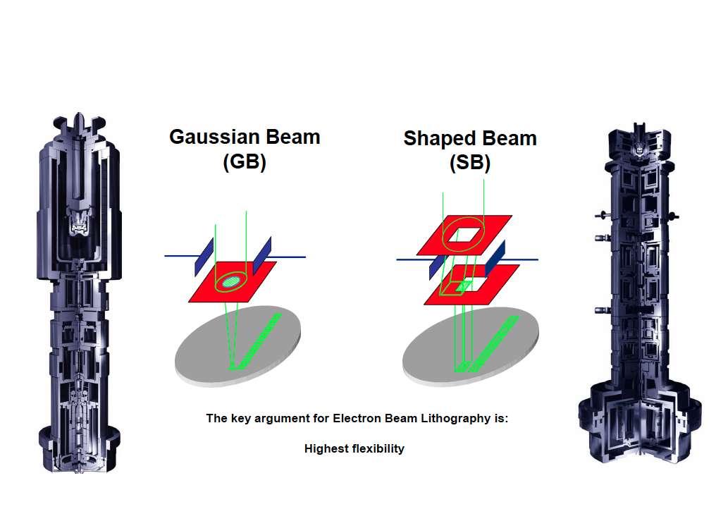
6 EBL configuration (Schottky FEG) UHV Selectable Aperture


7 Characteristics of EBL Typical characteristics: - High resolution < 10 nm - Flexible: direct write, maskless - Relatively slow

8 EBL exposure process Trend in research machines: 100 kev machines. less forward csattering, higher currents, higher dose, more back scattering


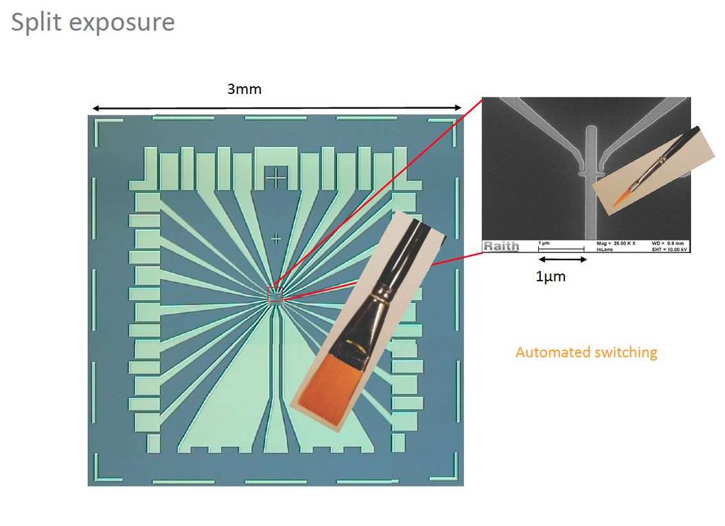
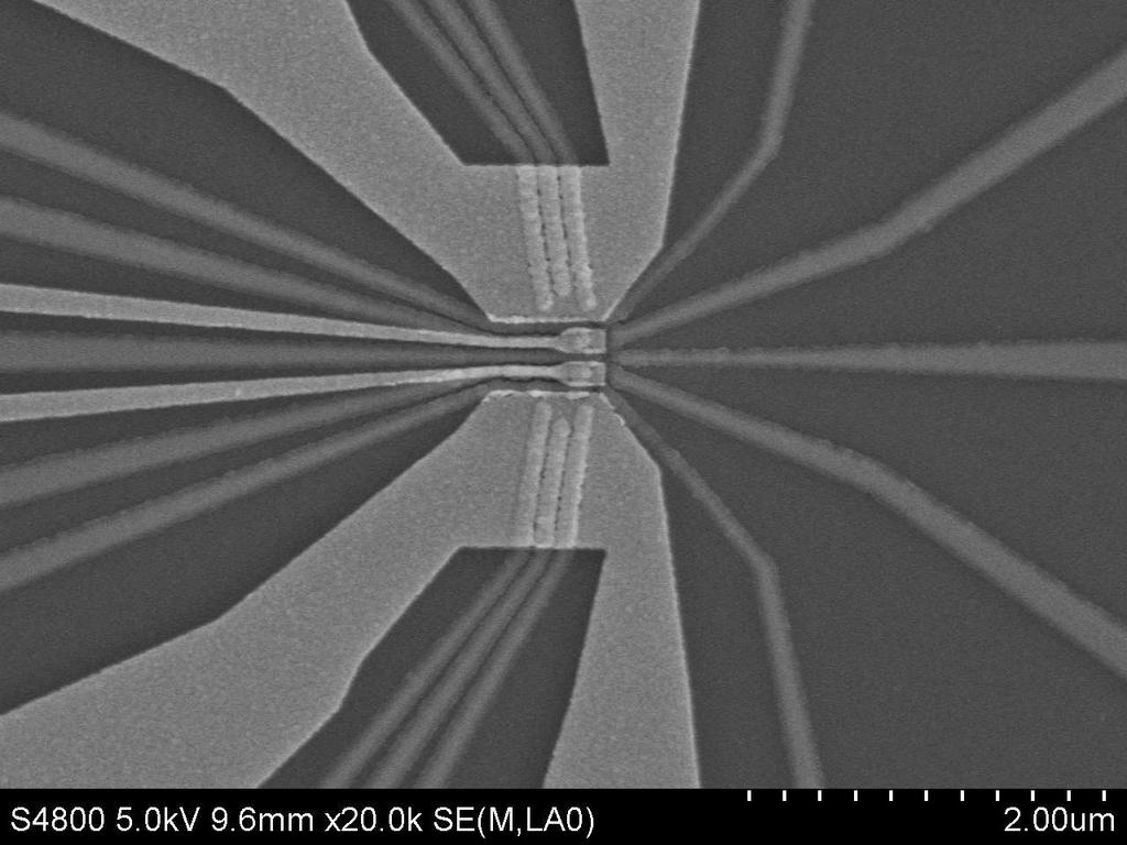
9 Gaussian Beam writing strategy Pattern split into fields Stage moves from field to field Primitive shapes filled by rastering Beam jumps between shapes Fast writing of sparse patterns stage movement Low throughput due to settling time Combination of high-res low-current and low-res high-current beams Application: R&D beam settling

10 Spot size determines maximum beam current e.g. for 20 nm features spot size < 5 nm
11
12 Electron Beam Lithography - key enabling technology in nanofabrication - Principles of Electron Beam Lithography (EBL) - Throughput - Applications in production - Applications in research - Conclusion
13 Throughput T x I = D x A T = time (s) I = beam current (A) D = dose (μc/cm 2 ) A = area (cm 2 ) CASE: 1 cm 2 writing with 20 nm resolution: (excl. stage movements and beam settling) I = 1 na D = 500 (μc/cm 2 ) A = 1 cm 2 T = 5 x 10 5 (s) = 6 days!!!!! Minimum dose in order to avoid shot noise Writing 10% of a 300 mm wafer: T > 1 year!!!!!
14 Shaped Beam writing Expose large areas with single "shots" of a shaped beam Programmable slits instead of aperture Extremely complex electron optical column Much faster than Gaussian spot systems Throughput limited by the pattern density Application: Mask writing Cell projection writing Use hole masks with more complex patterns ( cells ) to shape the beam Multiple cells in selectable aperture array Useful for highly repetitive designs with small unit cells
15

16 Summary of EBL writing methods


17 Multi-beam beams x 7x7 sub-beams = beams 10 WPH (300mm)
 Elionix")
 Raith")

")
 Multi-beam")
18 Gaussian Beam Crestec (Jp) Elionix (Jp) Jeol (Jp) Nanobeam (UK) Raith (Ge/NL) SEM M M 1-3 M Shaped Beam Advantest (Jp) NuFlare (Jp) Vistec Semi (Ge) Multi-beam Mapper (NL) IMS/Jeol (A) 10 M
19 Multi Beam Market data Market share Lithography Market M CARG 10% EBL < M Gaussian Beam EBL 100 M CARG 3% Cost euv EBL Wafer Size mm Fab 1000 < 50 M Litho tool 100 < 5 M Mask-set > 10 0 M Throughput > 100 < 1 WPH (300 mm) LVM Research

20 EBL at KavliNanolab Delft 1x Raith EBPG5000+ & 1x Raith EBPG5200 both with 10 holder load lock 24/7 operation 120 users 5000 hrs per machine for 6000 jobs (2015) 50nm
21 Electron Beam Lithography - key enabling technology in nanofabrication - Principles of Electron Beam Lithography (EBL) - Throughput - Applications in production - Applications in research - Conclusion


22 Product applications - T-gates for HEMTs (High Electron Mobility Transistors, high-power RF)

23 Blazed stacked X-ray zone plates


24 With kind permission of PSI Example, Multiple-Step HSQ Lithography Three consecutive e-beam exposures by a Vistec EBPG 5000plus tool for a two-level structure
25 Electron Beam Lithography - key enabling technology in nanofabrication - Principles of Electron Beam Lithography (EBL) - Throughput - Applications in production - Applications in research - Conclusion
26 50nm


27 Building a Quantum Computer Spin qubits quantum dots in GaAs and Si devices Group Lieven Vandersypen QuTech -TUDelft
28

29 Quantum Mediator double spin interaction through empty QD exchange the information between the two spins over a larger distance. Group Lieven Vandersypen QuTech -TUDelft Nature Nanotechnology, 10 October 2016.


30 Group Lieven Vandersypen QuTech -TUDelft

31 Building a Quantum Internet the instantaneous entanglement link - a radically new form of secure communications Loophole-free Bell test Group Ronald Hanson QuTech TUDelft Nature 526, (29 October 2015)

32 NV centers in diamond Nanofabrication by FIB and EBL Group Ronald Hanson QuTech -TUDelft

33 Large Scale Quantum Systems Mechanical Resonators for Quantum Optomechanics Experiments at Room Temperature Group Simon Gröblacher QN -TUDelft


34 ultra-thin silicon nitride tethered membranes - mechanical quality factors of around 10 8 at RT - reflectivities >99% (photonic crystal) Group Simon Gröblacher QN -TUDelft Phys. Rev. Lett. 116, (2016)

35 Single Molecule Quantum Devices mechanically controllable break junctions to study gate-tunable single-molecule diode Group Herre van der Zant QN TUDelft Nanoscale, 2016, 8, 8919

36 DPE-F2 Group Herre van der Zant QN TUDelft Nanoscale, 2016, 8, 8919
37 Conclusions - Great role for EBL in nanoscale research - Throughput EBL will remain a challenge - Opportunity for multi-beam techniques in production and research EBL Thanks to input from Raith and TU Delft groups in Kavli Institute for Nanoscience Delft
38
39
40 Nanopeople
NANO-FABRICATION FOR MESOSCOPIC PHYSICS
 NANO-FABRICATION FOR MESOSCOPIC PHYSICS Frédéric Pierre CNRS, Laboratory of Photonics and Nanostructures (LPN), Marcoussis, France ϕ Nano Team LPN PLAN Overview Electron beam lithography Step by step realization
Introduction to Lithography
 Introduction to Lithography G. D. Hutcheson, et al., Scientific American, 290, 76 (2004). Moore s Law Intel Co-Founder Gordon E. Moore Cramming More Components Onto Integrated Circuits Author: Gordon E.
Micro- and Nano-Technology... for Optics
 Micro- and Nano-Technology...... for Optics 3.2 Lithography U.D. Zeitner Fraunhofer Institut für Angewandte Optik und Feinmechanik Jena Electron Beam Column electron gun beam on/of control magnetic deflection
Single-digit-resolution nanopatterning with. extreme ultraviolet light for the 2.5 nm. technology node and beyond
 Electronic Supplementary Material (ESI) for Nanoscale. This journal is The Royal Society of Chemistry 205 Supplementary Information for: Single-digit-resolution nanopatterning with extreme ultraviolet
ECE280: Nano-Plasmonics and Its Applications. Week5. Extraordinary Optical Transmission (EOT)
") ECE280: Nano-Plasmonics and Its Applications Week5 Extraordinary Optical Transmission (EOT) Introduction Sub-wavelength apertures in metal films provide light confinement beyond the fundamental diffraction
ECE280: Nano-Plasmonics and Its Applications Week5 Extraordinary Optical Transmission (EOT) Introduction Sub-wavelength apertures in metal films provide light confinement beyond the fundamental diffraction
Sub-5 nm Structures Process Development and Fabrication Over Large Areas
 A S Jugessur,, 2017, 1:1 SciFed Nanotech Research Letters Research Article Open Access Sub-5 nm Structures Process Development and Fabrication Over Large Areas * A S Jugessur * University of Iowa Microfabrication
Examples of dry etching and plasma deposition at Glasgow University
 Examples of dry etching and plasma deposition at Glasgow University Glasgow has pioneered and established many novel research activities involving the development of new dry etch processes and dry etch
Simple method for formation of nanometer scale holes in membranes. E. O. Lawrence Berkeley National Laboratory, Berkeley, CA 94720
 Simple method for formation of nanometer scale holes in membranes T. Schenkel 1, E. A. Stach, V. Radmilovic, S.-J. Park, and A. Persaud E. O. Lawrence Berkeley National Laboratory, Berkeley, CA 94720 When
James Watt Nanofabrication Centre
 James Watt Nanofabrication Centre Prof Douglas Paul Director Douglas.Paul@glasgow.ac.uk The University of Glasgow Established in 1451 7 Nobel Laureates 16,500 undergraduates, 5,000 graduates and 5,000
Precise Ion and Electron Beam Processing for Nano-Structuring
 Precise Ion and Electron Beam Processing for Nano-Structuring Regina Korntner, Hans Loeschner and Elmar Platzgummer Vienna, Austria 1 Outline Short Introduction to IMS Technology Introduction History of
EUV Transmission Lens Design and Manufacturing Method
 1 EUV Transmission Lens Design and Manufacturing Method Kenneth C. Johnson kjinnovation@earthlink.net 7/16/2018 http://vixra.org/abs/1807.0188 Abstract This paper outlines a design for an EUV transmission
EECS130 Integrated Circuit Devices
 EECS130 Integrated Circuit Devices Professor Ali Javey 9/13/2007 Fabrication Technology Lecture 1 Silicon Device Fabrication Technology Over 10 15 transistors (or 100,000 for every person in the world)
Advanced resists for e-beam lithography: processing, exposure and characterization (Part II)
") Advanced resists for e-beam lithography: processing, exposure and characterization (Part II) Dra. Mariana Pojar de Melo Prof. Dr. Antonio Carlos Seabra Dep. Eng. de Sistemas Eletrônicos Escola Politécnica
Advanced resists for e-beam lithography: processing, exposure and characterization (Part II) Dra. Mariana Pojar de Melo Prof. Dr. Antonio Carlos Seabra Dep. Eng. de Sistemas Eletrônicos Escola Politécnica
Processing guidelines. Negative Tone Photoresists mr-ebl 6000
 Characteristics Processing guidelines Negative Tone Photoresists mr-ebl 6000 mr-ebl 6000 is a chemically amplified negative tone photoresist for the use in micro- and nanoelectronics. - Electron beam sensitive
LIFT-OFF TECHNIQUE USING DIFFERENT E-BEAM WRITERS. Jana CHLUMSKÁ, Vladimír KOLAŘÍK, Stanislav KRÁTKÝ, Milan MATĚJKA, Michal URBÁNEK, Miroslav HORÁČEK
 LIFT-OFF TECHNIQUE USING DIFFERENT E-BEAM WRITERS Jana CHLUMSKÁ, Vladimír KOLAŘÍK, Stanislav KRÁTKÝ, Milan MATĚJKA, Michal URBÁNEK, Miroslav HORÁČEK Institute of Scientific Instruments of the ASCR, v.
Nanofabrication Prof. Stephen Y. Chou NanoStructure Laboratory
 Nanofabrication Prof. Stephen Y. Chou Department of Electrical Engineering Princeton University 1 Acknowledgment Dr. Paul Fischer Dr. Yun Wang Dr. Jay Guo Dr. Peter Klauss Dr. Jim Wang Dr. Longtin He Dr.
PLASMONIC STRUCTURES IN PMMA RESIST
 PLASMONIC STRUCTURES IN PMMA RESIST Michal URBÁNEK a, Stanislav KRÁTKÝ a, MARCEL ŠIMÍK b, Vladimír KOLAŘÍK a, Miroslav HORÁČEK a, Milan MATĚJKA a a Institute of Scientific Instruments of the ASCR, v.v.i.,
Chapter 3 Silicon Device Fabrication Technology
 Chapter 3 Silicon Device Fabrication Technology Over 10 15 transistors (or 100,000 for every person in the world) are manufactured every year. VLSI (Very Large Scale Integration) ULSI (Ultra Large Scale
Contents. From microelectronics down to nanotechnology
 Contents From microelectronics down to nanotechnology sami.franssila@tkk.fi Lithography: scaling x- and y-dimensions MOS transistor physics Scaling oxide thickness (z-dimension) CNT transistors Conducting
Contents. From microelectronics down to nanotechnology. Top down nanotechnology. Writing patterns
 Contents From microelectronics down to nanotechnology sami.franssila@tkk.fi Lithography: scaling x- and y-dimensions MOS transistor physics Scaling oxide thickness (z-dimension) CNT transistors Conducting
Micro-Nano Fabrication Research
 Micro-Nano Fabrication Research Technical Education Quality Improvement Programme 22-23 December 2014 Dr. Rakesh G. Mote Assistant Professor Department of Mechanical Engineering IIT Bombay rakesh.mote@iitb.ac.in;
Ion Beam Technology. FIB Nanofabrication at Its Excellence
 Ion Beam Technology FIB Nanofabrication at Its Excellence High-Resolution and Versatile Focused Ion Beam Nanofabrication, Lithography and Nanoengineering FOCUSED ION BEAM NANOFABRICATION Cutting-edge research
Czochralski Crystal Growth
 Czochralski Crystal Growth Crystal Pulling Crystal Ingots Shaping and Polishing 300 mm wafer 1 2 Advantage of larger diameter wafers Wafer area larger Chip area larger 3 4 Large-Diameter Wafer Handling
From microelectronics down to nanotechnology.
 From microelectronics down to nanotechnology sami.franssila@tkk.fi Contents Lithography: scaling x- and y-dimensions MOS transistor physics Scaling oxide thickness (z-dimension) CNT transistors Conducting
EUV optics lifetime Radiation damage, contamination, and oxidation
 EUV optics lifetime Radiation damage, contamination, and oxidation M. van Kampen ASML Research 10-11-2016 Preamble Slide 2 ASML builds lithography scanners High-resolution photocopiers Copies mask pattern
Fabrication of Nanoscale Silicon Membranes on SOI Wafers Using Photolithography and Selective Etching Techniques:
 Fabrication of Nanoscale Silicon Membranes on SOI Wafers Using Photolithography and Selective Etching Techniques: Participant Names: Moriah Faint, Marcos Rodriguez Mentor: Frank Tsang Date: 1 Introduction
Unit title: Nanotechnology
 Unit title: Nanotechnology Unit code: K/601/0311 QCF level: 4 Credit value: 15 Aim This unit examines the role of nanotechnology at the interface of Chemistry, Biology, Physics and Engineering, especially
Physical Vapor Deposition (PVD) Zheng Yang
 Zheng Yang") Physical Vapor Deposition (PVD) Zheng Yang ERF 3017, email: yangzhen@uic.edu Page 1 Major Fabrication Steps in MOS Process Flow UV light Mask oxygen Silicon dioxide photoresist exposed photoresist oxide
Physical Vapor Deposition (PVD) Zheng Yang ERF 3017, email: yangzhen@uic.edu Page 1 Major Fabrication Steps in MOS Process Flow UV light Mask oxygen Silicon dioxide photoresist exposed photoresist oxide
EE40 Lec 22. IC Fabrication Technology. Prof. Nathan Cheung 11/19/2009
 Suggested Reading EE40 Lec 22 IC Fabrication Technology Prof. Nathan Cheung 11/19/2009 300mm Fab Tour http://www-03.ibm.com/technology/manufacturing/technology_tour_300mm_foundry.html Overview of IC Technology
FABRICATION ENGINEERING MICRO- NANOSCALE ATTHE AND. Fourth Edition STEPHEN A. CAMPBELL. of Minnesota. University OXFORD UNIVERSITY PRESS
 AND FABRICATION ENGINEERING ATTHE MICRO- NANOSCALE Fourth Edition STEPHEN A. CAMPBELL University of Minnesota New York Oxford OXFORD UNIVERSITY PRESS CONTENTS Preface xiii prrt i OVERVIEW AND MATERIALS
Electricity from the Sun (photovoltaics)
") Electricity from the Sun (photovoltaics) 0.4 TW US Electricity Consumption 100 100 square kilometers of solar cells could produce all the electricity for the US. But they are still too costly. The required
Electricity from the Sun (photovoltaics) 0.4 TW US Electricity Consumption 100 100 square kilometers of solar cells could produce all the electricity for the US. But they are still too costly. The required
ADVANCED NANOSCALE SCIENCE & ENGINEERING NANOPHYSICS SEMESTER MONTH CONTENT LAB THEMES SKILLS ASSESSMENTS. Cutting it Down to Nano Lab
 September Nano-Intro (Same topics for nanophysics and nanochem) Topic I: GOT NANO? Unit 1 Nano -Calculations Metric Review 2 Dimensional Analysis 3 Dimensional Analysis Sci. Not. & Sig. Figs. NanoDefinitions
SUPPLEMENTARY INFORMATIONS
 SUPPLEMENTARY INFORMATIONS Dynamic Evolution of Conducting Nanofilament in Resistive Switching Memories Jui-Yuan Chen, Cheng-Lun Hsin,,, Chun-Wei Huang, Chung-Hua Chiu, Yu-Ting Huang, Su-Jien Lin, Wen-Wei
Compact hybrid plasmonic-si waveguide structures utilizing Albanova E-beam lithography system
 Compact hybrid plasmonic-si waveguide structures utilizing Albanova E-beam lithography system Introduction Xu Sun Laboratory of Photonics and Microwave Engineering, Royal Institute of Technology (KTH),
Traceable Standard for Sub - 100nm Metrology
 University of Tennessee, Knoxville Trace: Tennessee Research and Creative Exchange Masters Theses Graduate School 5-2007 Traceable Standard for Sub - 100nm Metrology Sachin Jayant Deo University of Tennessee
More on VLSI Fabrication Technologies. Emanuele Baravelli
 More on VLSI Fabrication Technologies Emanuele Baravelli Some more details on: 1. VLSI meaning 2. p-si epitaxial layer 3. Lithography 4. Metallization 5. Process timings What does VLSI mean, by the way?
WP7 JRA2 JRA2 Research on High Precision Manufacturing. Investigation of optimum NIL stamp fabrication method to copy sub-10 nm BCP features
 DELIVERABLE REPORT WP7 JRA2 JRA2 Research on High Precision Manufacturing D7.1 Investigation of optimum NIL stamp fabrication method to copy sub-10 nm BCP features M18 NFFA-Europe has received funding
EUV Transmission Lens Design and Manufacturing Method
 1 EUV Transmission Lens Design and Manufacturing Method Kenneth C. Johnson kjinnovation@earthlink.net 7/9/2018 Abstract This paper outlines a design for an EUV transmission lens comprising blazed, phase-
Supporting Information for Effects of Thickness on the Metal-Insulator Transition in Free-Standing Vanadium Dioxide Nanocrystals
 Supporting Information for Effects of Thickness on the Metal-Insulator Transition in Free-Standing Vanadium Dioxide Nanocrystals Mustafa M. Fadlelmula 1,2, Engin C. Sürmeli 1,2, Mehdi Ramezani 1,2, T.
Integration of Block-Copolymer with Nano- Imprint Lithography: Pushing the Boundaries of Emerging Nano-Patterning Technology
 Integration of Block-Copolymer with Nano- Imprint Lithography: Pushing the Boundaries of Emerging Nano-Patterning Technology April 2010 update SNL Geoff Brennecka (PI) Bruce Burckel Matt George Jack Skinner
Our Future. Professor Umesh K. Mishra,
 Small Wonders in Our Future Professor Umesh K. Mishra, Director of the ONR Center for Advanced Nitride Electronics (CANE) and the AFOSR Center for Radiation Hard Physics University of California, Santa
EE6303 LINEAR INTEGRATED CIRCUITS AND APPLICATIONS 2 MARK QUESTIONS WITH ANSWERS UNIT I IC FABRICATION
 SRI VENKATESWARA COLLEGE OF ENGINEERING AND TECHNOLOGY TIRUPACHUR DEPARTMENT OFELECTRICAL AND ELECTRONICS ENGINEERING EE6303 LINEAR INTEGRATED CIRCUITS AND APPLICATIONS 1. Define an Integrated circuit.
Supporting Information for: Plasmonic Nanopores. for Trapping, Controlling Displacement, and. Sequencing of DNA
 Supporting Information for: Plasmonic Nanopores for Trapping, Controlling Displacement, and Sequencing of DNA Maxim Belkin, Shu-Han Chao, Magnus P. Jonsson,,, Cees Dekker,, and Aleksei Aksimentiev, Department
Nanoimprinting in Polymers and Applications in Cell Studies. Albert F. YEE Chemical Engineering & Materials Science UC Irvine
 Nanoimprinting in Polymers and Applications in Cell Studies Albert F. YEE Chemical Engineering & Materials Science UC Irvine Presentation outline Motivation Reversal imprinting Soft inkpad imprinting on
THE IMPACT OF 3D DEVICES ON THE FUTURE OF PROCESS MATERIALS TRENDS & OPPORTUNITIES
 THE IMPACT OF 3D DEVICES ON THE FUTURE OF PROCESS MATERIALS TRENDS & OPPORTUNITIES L. Shon Roy K. Holland, PhD. October 2014 Materials Examples Process materials used to make semiconductor devices Gases
Fabrication and Layout
 ECEN454 Digital Integrated Circuit Design Fabrication and Layout ECEN 454 3.1 A Glimpse at MOS Device Polysilicon Aluminum ECEN 475 4.2 1 Material Classification Insulators Glass, diamond, silicon oxide
Fabrication characteristics of a line-and-space pattern and a dot pattern on a roll mold by using electron-beam lithography
 0123456789 Bulletin of the JSME Journal of Advanced Mechanical Design, Systems, and Manufacturing Vol.10, No.5, 2016 Fabrication characteristics of a line-and-space pattern and a dot pattern on a roll
Lithography options for the 32nm half pitch node. imec
 Lithography options for the 32nm half pitch node imec 2006 1 Lithography options for the 32nm half pitch node Luc Van den hove and Kurt Ronse ITRS roadmap:32 nm half pitch requirement Product Half-Pitch,
Fabrication of photonic band-gap crystals
 Fabrication of photonic band-gap crystals C. C. Cheng and A. Scherer California Institute of Technology, Pasadena, California 91125 Received 19 June 1995; accepted 9 August 1995 We describe the fabrication
Supplementary Figure S1 Photograph of MoS 2 and WS 2 flakes exfoliated by different metal naphthalenide (metal = Na, K, Li), and dispersed in water.
, and dispersed in water.") Supplementary Figure S1 Photograph of MoS 2 and WS 2 flakes exfoliated by different metal naphthalenide (metal = Na, K, Li), and dispersed in water. Supplementary Figure S2 AFM measurement of typical LTMDs
Supplementary Figure S1 Photograph of MoS 2 and WS 2 flakes exfoliated by different metal naphthalenide (metal = Na, K, Li), and dispersed in water. Supplementary Figure S2 AFM measurement of typical LTMDs
EE 5611 Introduction to Microelectronic Technologies Fall Tuesday, September 04, 2012 Lecture 01
 EE 5611 Introduction to Microelectronic Technologies Fall 2012 Tuesday, September 04, 2012 Lecture 01 1 Instructor: Jing Bai Contact Email: jingbai@d.umn.edu, hone: (218)726-8606, Office: MWAH 255 Webpage:
Tunable Nanoscale Plasmon Antenna for Localization and Enhancement of Optical Energy. Douglas Howe
 Tunable Nanoscale Plasmon Antenna for Localization and Enhancement of Optical Energy Douglas Howe Applied Optics Spring 2008 Table of Contents Abstract... 3 Introduction... 4 Surface Plasmons... 4 Nano
Electron Beam Induced Processes and their Applicability to Mask Repair
 & Electron Beam Induced Processes and their Applicability to Mask Repair Hans W.P. Koops (1), Volker Boegli (1), Klaus Edinger (1), Johannes Bihr (2), Jens Greiser (2), (1) NaWoTec GmbH Rossdorf Germany
Crystallographic Characterization of GaN Nanowires by Raman Spectral Image Mapping
 Crystallographic Characterization of GaN Nanowires by Raman Spectral Image Mapping Heerad Farkhoor, Adam Schwartzberg, Jeffrey Urban August 12, 2009 Abstract Obtaining structural information of nano-structured
CMOS Fabrication. Dr. Bassam Jamil. Adopted from slides of the textbook
 CMOS Fabrication Dr. Bassam Jamil Adopted from slides of the textbook CMOS Fabrication CMOS transistors are fabricated on silicon wafer Lithography process similar to printing press On each step, different
Lecture 22: Integrated circuit fabrication
 Lecture 22: Integrated circuit fabrication Contents 1 Introduction 1 2 Layering 4 3 Patterning 7 4 Doping 8 4.1 Thermal diffusion......................... 10 4.2 Ion implantation.........................
Cold-developed electron-beam-patterned Zep 7000 for fabrication of 13-nm nickel zone plates
 Cold-developed electron-beam-patterned Zep 7000 for fabrication of 13-nm nickel zone plates Julia Reinspach, Magnus Lindblom, Olov von Hofsten, Michael Bertilson, Hans M. Hertz, and Anders Holmberg Department
Chemically Tunable Full Spectrum Optical Properties of 2D Silicon Telluride Nanoplates
 SUPPORTING INFORMATION Chemically Tunable Full Spectrum Optical Properties of 2D Silicon Telluride Nanoplates Mengjing Wang,, Gabriella Lahti, David Williams, and Kristie J. Koski * Department of Chemistry,
Technology process. It s very small world. Electronics and Microelectronics AE4B34EM. Why is the integration so beneficial?
 It s very small world Electronics and Microelectronics AE4B34EM 9. lecture IC processing technology Wafer fabrication Lithography How to get 1 000 000 000 Components to 1 cm 2 Human hair on the surface
VLSI INTRODUCTION P.VIDYA SAGAR ( ASSOCIATE PROFESSOR) Department of Electronics and Communication Engineering, VBIT
 Department of Electronics and Communication Engineering, VBIT") VLSI INTRODUCTION P.VIDYA SAGAR ( ASSOCIATE PROFESSOR) contents UNIT I INTRODUCTION: Introduction to IC Technology MOS, PMOS, NMOS, CMOS & BiCMOS technologies. BASIC ELECTRICAL PROPERTIES : Basic Electrical
VLSI INTRODUCTION P.VIDYA SAGAR ( ASSOCIATE PROFESSOR) contents UNIT I INTRODUCTION: Introduction to IC Technology MOS, PMOS, NMOS, CMOS & BiCMOS technologies. BASIC ELECTRICAL PROPERTIES : Basic Electrical
Nanofabrication of p-type GaAs by AFM-based surface oxidation process and its application to planar-type devices
 Nanofabrication of p-type GaAs by AFM-based surface oxidation process and its application to planar-type devices Yuichi Matsuzaki, Shin-ya Kamada, Akira Yamada and Makoto Konagai Department of Physical
ECCI of AlGaN/GaN HEMT structures grown on Si
 ECCI of AlGaN/GaN HEMT structures grown on Si D. Thomson 1, G. Naresh-Kumar 1, B. Hourahine 1, C. Trager-Cowan 1, P. Wright 2 and T. Martin 2 1 Dept. Of Physics, SUPA, University of Strathclyde, Glasgow
2008 Summer School on Spin Transfer Torque
 2008 Summer School on Spin Transfer Torque Nano-scale device fabrication 2-July-2008 Byoung-Chul Min Center for Spintronics Research Korea Institute of Science and Technology Introduction Moore s Law
Key Technologies for Next Generation EUV Lithography
 Key Technologies for Next Generation EUV Lithography September 15, 2017 Toshi Nishigaki Vice President and General Manager Advanced Semiconductor Technology Division / Tokyo Electron Limited Toshi Nishigaki
Introduction to Nanoscience and Nanotechnology
 Introduction to Nanoscience and Nanotechnology ENS 463 2. Principles of Nano-Lithography by Alexander M. Zaitsev alexander.zaitsev@csi.cuny.edu Tel: 718 982 2812 Office 4N101b 1 Lithographic patterning
Microstructure of Electronic Materials. Amorphous materials. Single-Crystal Material. Professor N Cheung, U.C. Berkeley
 Microstructure of Electronic Materials Amorphous materials Single-Crystal Material 1 The Si Atom The Si Crystal diamond structure High-performance semiconductor devices require defect-free crystals 2 Crystallographic
Nanoscale Imaging, Material Removal and Deposition for Fabrication of Cutting-edge Semiconductor Devices
 Hitachi Review Vol. 65 (2016), No. 7 233 Featured Articles Nanoscale Imaging, Material Removal and Deposition for Fabrication of Cutting-edge Semiconductor Devices Ion-beam-based Photomask Defect Repair
3. Overview of Microfabrication Techniques
 3. Overview of Microfabrication Techniques The Si revolution First Transistor Bell Labs (1947) Si integrated circuits Texas Instruments (~1960) Modern ICs More? Check out: http://www.pbs.org/transistor/background1/events/miraclemo.html
Supporting Online Material for
 www.sciencemag.org/cgi/content/full/327/5961/60/dc1 Supporting Online Material for Polarization-Induced Hole Doping in Wide Band-Gap Uniaxial Semiconductor Heterostructures John Simon, Vladimir Protasenko,
Fabrication and Characterization of Two-Dimensional Photonic. Crystal Microcavities in Nanocrystalline Diamond
 Fabrication and Characterization of Two-Dimensional Photonic Crystal C. F. Wang, a),b) R. Hanson, a) D. D. Awschalom, a)c) E. L. Hu c),d) University of California, Santa Barbara, California 93106 T. Feygelson,
High Dose Hydrogen Implant Blistering Effects As a Function of Selected Implanter And Substrate Conditions
 As submitted - IIT 06 Implant Conference High Dose Hydrogen Implant Blistering Effects As a Function of Selected Implanter And Substrate Conditions Ronald Eddy a, Chuck Hudak a, Pamla Bettincurt b, Sandra
ELEC 3908, Physical Electronics, Lecture 4. Basic Integrated Circuit Processing
 ELEC 3908, Physical Electronics, Lecture 4 Basic Integrated Circuit Processing Lecture Outline Details of the physical structure of devices will be very important in developing models for electrical behavior
Lecture #18 Fabrication OUTLINE
 Transistors on a Chip Lecture #18 Fabrication OUTLINE IC Fabrication Technology Introduction the task at hand Doping Oxidation Thin-film deposition Lithography Etch Lithography trends Plasma processing
EE 5611 Introduction to Microelectronic Technologies Fall Tuesday, September 02, 2014 Lecture 01
 EE 5611 Introduction to Microelectronic Technologies Fall 2014 Tuesday, September 02, 2014 Lecture 01 1 Instructor: Jing Bai Contact Email: jingbai@d.umn.edu, hone: (218)726-8606, Office: MWAH 255 Webpage:
Success story of the CSAR 62 - or a high-tech resist makes its way
 Success story of the CSAR 62 - or a high-tech resist makes its way The constant strive for more and more powerful computers is correlated with the demand for increasingly smaller structures in the manufacture
NRL Institute for Nanoscience 1 May 2012
 NRL Institute for Nanoscience 1 May 2012 Dr. Eric S. Snow, Director The Naval Research Laboratory Highly interdisciplinary laboratory Research Focus Areas Battlespace Environments, Undersea Warfare, Space
Nanotechnology makes brighter LED s. Michael P.C. Watts
 Nanotechnology makes brighter LED s Michael P.C. Watts www.impattern.com Outline Why are LED s such a big deal? Brightness; lumens per watt & lumens per dollar Applications How does nanotechnology help?
ECE 440 Lecture 27 : Equilibrium P-N Junctions I Class Outline:
 ECE 440 Lecture 27 : Equilibrium P-N Junctions I Class Outline: Fabrication of p-n junctions Contact Potential Things you should know when you leave Key Questions What are the necessary steps to fabricate
Lecture 0: Introduction
 Lecture 0: Introduction Introduction Integrated circuits: many transistors on one chip. Very Large Scale Integration (VLSI): bucketloads! Complementary Metal Oxide Semiconductor Fast, cheap, low power
JSM-7800F Field Emission Scanning Electron Microscope
 JSM-7800F catalogue JSM-7800F Field Emission Scanning Electron Microscope We provide high performance The Ultimate Research Tool for Multi-Disciplinary Research Institutions Extreme resolution The super
VLSI Digital Systems Design
 VLSI Digital Systems Design CMOS Processing cmpe222_03process_ppt.ppt 1 Si Purification Chemical purification of Si Zone refined Induction furnace Si ingot melted in localized zone Molten zone moved from
Hydrogen silsesquioxaneõnovolak bilayer resist for high aspect ratio nanoscale electron-beam lithography
 Hydrogen silsesquioxaneõnovolak bilayer resist for high aspect ratio nanoscale electron-beam lithography Falco C. M. J. M. van Delft a) and Jos P. Weterings Philips Research Laboratories, Prof. Holstlaan
لبا ب ةعماج / ةيساسلأا ةيبرتلا ةيلك ة لجم
 Photoluminescence from Etched Silicon Surface by High Power Laser Oday A. Abbass Department of Physics/College of Sciences/University of Kufa ABSTRACT Porous silicon layers (P-Si) has been prepared in
Lecture 2: CMOS Fabrication Mark McDermott Electrical and Computer Engineering The University of Texas at Austin
 Lecture 2: CMOS Fabrication Mark McDermott Electrical and Computer Engineering The University of Texas at Austin Agenda Last module: Introduction to the course How a transistor works CMOS transistors This
Electron Beam Lithography patterned Hydrogen Silsesquioxane (HSQ) resist as a mandrel for Self- Aligned Double Patterning application
 resist as a mandrel for Self- Aligned Double Patterning application") Electron Beam Lithography patterned Hydrogen Silsesquioxane (HSQ) resist as a mandrel for Self- Aligned Double Patterning application Running title: EBL patterned HSQ resist as a mandrel for SADP application
Electron Beam Lithography patterned Hydrogen Silsesquioxane (HSQ) resist as a mandrel for Self- Aligned Double Patterning application Running title: EBL patterned HSQ resist as a mandrel for SADP application
Point-contacting by Localised Dielectric Breakdown: A new approach for contacting solar cells
 Point-contacting by Localised Dielectric Breakdown: A new approach for contacting solar cells SPREE Public Seminar 20 th February 2014 Ned Western Supervisor: Stephen Bremner Co-supervisor: Ivan Perez-Wurfl
Preface Preface to First Edition
 Contents Foreword Preface Preface to First Edition xiii xv xix CHAPTER 1 MEMS: A Technology from Lilliput 1 The Promise of Technology 1 What Are MEMS or MST? 2 What Is Micromachining? 3 Applications and
Rare-Earth Ions in Niobium-based Devices as a Quantum Memory
 TECHNICAL REPORT 3050 September 2016 Rare-Earth Ions in Niobium-based Devices as a Quantum Memory Magneto-Optical Effects on Room Temperature Electrical Transport Vincent DinH Brad Liu Dave Rees Kenneth
Applications. SIMS successfully applied to many fields. Catalysts, metals, ceramics, minerals may primarily use imaging
 Applications SIMS successfully applied to many fields Catalysts, metals, ceramics, minerals may primarily use imaging Semiconductors extensively use depth profiling Si, GaAs, GaN, ZnO Minerals Analysis
A discussion of crystal growth, lithography, etching, doping, and device structures is presented in
 Chapter 5 PROCESSING OF DEVICES A discussion of crystal growth, lithography, etching, doping, and device structures is presented in the following overview gures. SEMICONDUCTOR DEVICE PROCESSING: AN OVERVIEW
EUV Technology, Martinez, CA
 Compact in-line EUV Laser Plasma Reflectometer for the measurement reflectivity and uniformity of EUV Lithography Mask Blank Multilayer Coatings Rupert C. C. Perera & James H. Underwood EUV Technology,
EUV Products and Business Opportunity
 EUV Products and Business Opportunity Christophe Fouquet Executive Vice President Business Line EUV ASML EUV Lithography product and business opportunity Key Messages ASML EUV lithography extends our Logic
STATE-OF-THE-ART OF FOCUSED ION BEAM NANOLITHOGRAPHY
 Journal of Optoelectronics and Advanced Materials,Vol. 7, No. 1, February 2005, p. 193-198 Invited Paper STATE-OF-THE-ART OF FOCUSED ION BEAM NANOLITHOGRAPHY K. Arshak *, M. Mihov a Electronic & Computer
EUV Products and Business Opportunity
 EUV Products and Business Opportunity Christophe Fouquet Executive Vice President Business Line EUV ASML EUV Lithography product and business opportunity Key Messages ASML EUV lithography extends our Logic
In-situ TEM observation of gold nanogaps by electromigration
 In-situ TEM observation of gold nanogaps by electromigration *Yosuke Murakami 1), Hayato Ochi 2), Masashi Arita 3), Kouichi Hamada 4), Yasuo Takahashi 5) and Seiji Takeda 6) 1), 2), 3), 4), 5) Graduate
Control of buckling in large nanomembranes using engineered support structures
 Control of buckling in large nanomembranes using engineered support structures Eiji Iwase 1, Pui-Chuen Hui 1, David Woolf 1, Alejandro W. Rodriguez 1,2, Steven G. Johnson 2, Federico Capasso 1, Marko Loncar
Improvement of silicon waveguide transmission by advanced e-beam lithography data fracturing strategies
 Improvement of silicon waveguide transmission by advanced e-beam lithography data fracturing strategies Running title: Improve silicon waveguide transmission by fracturing strategies Running Authors: N.
EPITAXY extended single-crystal film formation on top of a crystalline substrate. Homoepitaxy (Si on Si) Heteroepitaxy (AlAs on GaAs)
 Heteroepitaxy (AlAs on GaAs)") extended single-crystal film formation on top of a crystalline substrate Homoepitaxy (Si on Si) Heteroepitaxy (AlAs on GaAs) optoelectronic devices (GaInN) high-frequency wireless communication devices
extended single-crystal film formation on top of a crystalline substrate Homoepitaxy (Si on Si) Heteroepitaxy (AlAs on GaAs) optoelectronic devices (GaInN) high-frequency wireless communication devices
Nanoscale Materials Inspires Innovation and Drives Economic Development
 Nanoscale Materials Inspires Innovation and Drives Economic Development 5nm Greg Salamo & Alex Biris InAs Quantum Dots What is Nanoscience? The effort to understand and design structures at the nano size
Conductive Resists for Nanofabrication on Insulating Substrates
 Conductive Resists for Nanofabrication on Insulating Substrates by Farhan Hasan A thesis submitted to the University of Birmingham for the degree of DOCTOR OF PHILOSOPHY School of Chemical Engineering