ESA s approach to quality control of the supply chain for PCBs. Stan Heltzel European Space Agency
|
|
|
- Diana Brooks
- 5 years ago
- Views:
Transcription

1 ESA s approach to quality control of the supply chain for PCBs Stan Heltzel European Space Agency
2 Outline A. ESA s approach to supply chain control for PCBs B. Case study: contamination in PCBs 1. Problem description 2. Risk mitigations 2
3 ESA Projects: NRB, RFx, reviews Qualification: Test, Audit, NCR ECSS: Standardisation PCB/SMT WG: Harmonisation R&D PCB manufacturer Procurement: DR + MRR, Test, NCR Equipment manufacturer 3
4 ECSS European Cooperation for Space Standardisation ECSS-Q-ST-70-10C PCB qualifcation (revision ongoing) ECSS-Q-ST-70-11C PCB procurement (revision ongoing) ECSS-Q-ST-70-12C PCB design (first issued July 2014) In addition, Process Identification Documents (PID) describe qualified technology domain of each PCB manufatcurer. 4
5 Harmonisation of electronic technologies ECSS standardisation ecss.nl PCB/SMT WG with industry in the Component Technology Board technology roadmaps escies.org, spacecomponents.org 5
6 Technology drivers PCB are platform for placement and routing for complex components PCB Area Array Device ~2 keuro ~20 keuro PCBs need to be comparable to components in terms of reliability and complexity, but for a much lower cost. High pint count causes complex routing Miniaturization requires dense routing Signal integrity requires short routing 6
7 Reliability issues PCB material selection driven by assembly and repair, not by space environment PCB build-up driven by capability and miniaturization, not by manufacturability Material, build-up and metallisation processes affect reliability of interconnections Design and manufacturability are key 7
8 Qualification - Request for qualification: support, market, ESA projects - Qualification ECSS-Q-ST Audit - Qualified domain published in PID and on escies.org/pcb/ - Design & Procurement by OEMs - Periodic audit and re-qualification 8
9 ESA Projects: NRB, RFx, reviews Qualification: Test, Audit, NCR ECSS: Standardisation PCB/SMT WG: Harmonisation R&D PCB manufacturer Procurement: DR + MRR, Test, NCR Equipment manufacturer 9
10 B. Case study: contamination - Outline 1. Problem description a. Latent short circuit failure b. Failure mechanism c. Contamination d. IR testing 2. Risk mitigations a. Design b. Manufacture c. Base material supply 10


11 1. Latent short circuit - Introduction Short circuit failure occurred in PCBs for power distribution after prolonged functional testing in ambient lab environment or after thermal vacuum cycles. 11
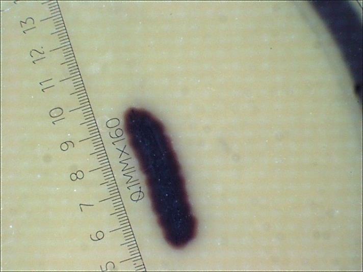
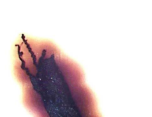
 Conductive Anodic")
12 1. Latent short circuit - Failure Mechanism Electromigration caused by: Pathway Electrolyte Bias voltage Dendritic growth (SIR) Conductive Anodic Filament 12


13 1. Latent short circuit - Pathway Resin-glass interface Hollow glass fibers Congolmerated flame retardant or fillers Delamination Voids Cracks [EA-2010-MAT-12B] Contamination by foreign material 13


14 1. Latent short circuit - Contamination Sources: PCB manufacturing processes Base material supply Types: Cl-bearing particles Metallic debris Organic residue Dust Fibers FR4 resin dust in polyimide etc 14

15 1. Latent short circuit IR test sistance_dieelectric_materials_ipc.pdf fiber contaminated no contamination observed T0 after 200TC after 500TC T0 after 200TC after 500TC 15


16 1. Latent short circuit IR test conclusions Fiber contamination provides pathway for electromigration 16
17 2. Risk mitigation PCB design IPC-2221 ECSS-Q-ST Space product assurance PCB design Example: 4 mil laminate with 2 oz Cu can have a min projected peak-to-peak dielectric thickness of 68 µm. Take account of tolerances in dielectric thickness Take account of etching tolerances for in-plane clearances Margin for double insulation of critical signals Presence of non-functional pads 2 sheets of glass reinforcement between copper layers 17


18 2. Risk mitigation PCB manufacturer a) Incoming sample inspection on base laminate 18


19 2. Risk mitigation PCB manufacturer b) Inspection on etched inner layers: 100% visual inspection on light table 19


20 2. Risk mitigation PCB manufacturer b) Inspection on etched inner layers: AOI 20
21 2. Risk mitigation PCB manufacturer c) Cleanliness control plan QT/2013/730/SH Recommendations: Cleanliness control between Cu oxidation and lay-up Restrictions on the use of materials that show static charging Class cleanroom in lay-up area Class cleanroom on flow bench De-ionisation equipment at lay-up 21

22 2. Risk mitigation PCB manufacturer d) Cleaning and inspection of ecthed inner layers and prepreg Clean tacky roller vacuum hovering Inspect UV fluorescence bright light 22


23 2. Risk mitigation PCB manufacturer e) Inspection on external layers Note: these are laminates, not prepreg 23
24 2. Risk mitigation PCB manufacturer f) High resistance electrical testing IPC-9252 IPC6012 class 3/a QT/2013/681/SH 10 V 250 V 250 V 10 MΩ 100 MΩ 1 GΩ V drop during ramp up is a failure Direct resistive testing 1.27 mm adjacency 24


25 2. Risk mitigation IPC-4101 base laminate Test frequency Pass/fail criteria Consequences of failure 25
26 2. Risk mitigation IPC-4101 base laminate Proposal for cleaner class of base materials [QT/2013/378/SH] Prepreg delivered as b-stage cured sheets Prepreg for manufacture of laminate Increase inspection frequency to 100% Laminate Reduce permittable fibre length from 13 mm to 0.5 mm Increase sample frequency to 2% Reject entire lot if test is non-compliant 26
27 Conclusions Interactions in supply chain identified contamination problems. Risk mitigations specified in design, manufacture and base material supply. New procurement specification in use and proposed to IPC

28 Thank you for your attention!
Latent Short Circuit Failure in High-rel PCBS Caused by Lack of Cleanliness of PCB Processes and Base Materials
 As originally published in the IPC APEX EXPO Conference Proceedings. Latent Short Circuit Failure in High-rel PCBS Caused by Lack of Cleanliness of PCB Processes and Base Materials Stan Heltzel, European
How Printed Circuit Boards are Made. Todd Henninger Field Applications Engineer Midwest Region
 PCB 101: How Printed Circuit Boards are Made Todd Henninger Field Applications Engineer Midwest Region Tooling PRE-PRODUCTION ENGINEERING (Tooling) Design Data Package CAD Data (ODB++ or Gerber 274x format)
IBM Laminate Study Group
 IBM Laminate Study Group Lead-Free Laminate Robustness Brett Krull, Dept FM2 Nov 18, 2009 Agenda Introductions Laminate Robustness Background Qualification Methods Contributing Factors Past Work on Laminate
Low CTE / High Tg FR-4 with High Heat Resistance
 Low CTE / High Tg FR-4 with High Heat Resistance Laminate: EM-827 Prepreg: EM-827B 1 Features Tg(DSC) > 170 Z direction CTE < 3.0% (50~260 ) High thermal degradation temperature: Td > 340 Excellent thermal
DURAVER -E-Cu quality 104 ML
 J B-DE 104 ML DURAVER -E-Cu quality 104 ML Base materials for multilayers 2 Quality and security to give you the edge The demands imposed with regard to the performance of circuit boards are rising constantly,
LEAD-FREE ASSEMBLY COMPATIBLE PWB FABRICATION AND ASSEMBLY PROCESSING GUIDELINES.
 LEAD-FREE ASSEMBLY COMPATIBLE PWB FABRICATION AND ASSEMBLY PROCESSING GUIDELINES. TECHNICAL BULLETIN As the industry has moved to lead-free assembly processing, the performance demands on the lead free
Offshore Wind Turbines Power Electronics Design and Reliability Research
 Offshore Wind Turbines Power Electronics Design and Reliability Research F. P. McCluskey CALCE/Dept. Of Mechanical Engineering University of Maryland, College Park, MD (301) 405-0279 mcclupa@umd.edu 1
Specification for Base Materials for Rigid and Multilayer Printed Boards
 ASSOCIATION CONNECTING ELECTRONICS INDUSTRIES Specification for Base Materials for Rigid and Multilayer Printed Boards Developed by the Laminate/Prepreg Materials Subcommittee (3-11) of the Printed Board
NP-180R NAN YA PLASTICS CORPORATION ELECTRONIC MATERIALS DIVISION. COPPER CLAD LAMINATE DEPARTMENT NO TUNG HWA N. ROAD, TAIPEI, TAIWAN.
 New: 2014/04/30 flame retardant copper clad laminate NP-180R High Tg 175 (DSC) Excellent dimensional stability through-hole reliability Excellent electrical, chemical and heat resistance properties IPC-4101C
Interconnection Reliability of HDI Printed Wiring Boards
 Presented in the ECWC 10 Conference at IPC Printed Circuits Expo, SMEMA Council APEX and Designers Summit 05 Interconnection Reliability of HDI Printed Wiring Boards Tatsuo Suzuki Nec Toppan Circuit Solutions,
B-IS400 IS420/3 IS400 IS420 PCL370HR. Temperature resistant mid and high T g - base materials with low z-axis expansion CAF ENHANCED
 J B-IS4 IS42/3 IS4 IS42 PCL37HR Temperature resistant mid and high T g - base materials with low z-axis expansion CAF ENHANCED Temperature-resistant base materials with low z-axis expansion IS4, IS42 and
Passive component embedding in printed circuit boards for space applications
 Passive component embedding in printed circuit boards for space applications 2nd Space Passive Component Days (SPCD), International Symposium 12-14 October 2016 ESA/ESTEC, Noordwijk, The Netherlands Maarten
Verifying The Reliability Of Connections In HDI PWBs
 Verifying The Reliability Of Connections In HDI PWBs The stacking of via holes is used effectively in the development of high density circuits on build-up printed wiring boards (PWBs). However, when micro
Building HDI Structures using Thin Films and Low Temperature Sintering Paste
 Building HDI Structures using Thin Films and Low Temperature Sintering Paste Catherine Shearer, James Haley and Chris Hunrath Ormet Circuits Inc. - Integral Technology California, USA chunrath@integral-hdi.com
Modeling Printed Circuit Boards with Sherlock 3.2
 Modeling Printed Circuit Boards with Sherlock 3.2 DfR Solutions September 23, 2014 Presented by: Dr. Nathan Blattau Senior Vice President 9000 Virginia Manor Rd Ste 290, Beltsville MD 20705 301-474-0607
SELECTIVE SOLDERING DESIGN FOR RELIABILITY USING A NOVEL TEST BOARD AND SIR TEST METHOD
 As originally published in the SMTA Proceedings SELECTIVE SOLDERING DESIGN FOR RELIABILITY USING A NOVEL TEST BOARD AND SIR TEST METHOD Mike Bixenman and David Lober KYZEN Corporation TN, USA mikeb@kyzen.com
UL PCB Recognition what is it & why do you need to know about it
 UL PCB Recognition what is it & why do you need to know about it Presented by Emma Hudson NCAB Customer Event March 2015 UL and the UL logo are trademarks of UL LLC 2015 Agenda What is UL and what are
Yash Sutariya President
 Yash Sutariya President Saturn Electronics Corporation Glory Faith North America Saturn Flex Systems Key Inputs to PCB Reliability Backbone Fabrication Processes Multilayer Press Via Drilling Copper Through
FABRICATING HIGH CURRENT, HEAVY COPPER PCBS
 Royal Circuit Solutions 21 Hamilton Ct, Hollister, CA 95023 (831) 636-7728 www.royalcircuits.com FABRICATING HIGH CURRENT, HEAVY COPPER PCBS INTRODUCTION All printed circuit boards (PCBs) carry current
Qualification and Performance Specification for High Frequency (Microwave) Printed Boards
 Printed Boards") Qualification and Performance Specification for High Frequency (Microwave) Printed Boards Developed by the High Speed/High Frequency Board Performance Subcommittee (D-22) of the High Speed/High Frequency
Qualification and Performance Specification for High Frequency (Microwave) Printed Boards Developed by the High Speed/High Frequency Board Performance Subcommittee (D-22) of the High Speed/High Frequency
A Novel Material for High Layer Count and High Reliability Printed Circuit Boards
 A Novel Material for High Layer Count and High Reliability Printed Circuit Boards Jie Wan, Junqi Tang, Xianping Zeng Shengyi Technology Co., Ltd. No.5 Western Industry Road, North Industry District SSL
Company Overview Markets Products- Capabilities
 Company Overview Markets Products- Capabilities A Simpler way for PCB production. www.purepcb.co.uk What can Pure do for you? From 1 off Circuit upward, No MOQ/MOV High Mix Production Focus. Fast Turn
IPC-6012DA with Amendment 1. Automotive Applications Addendum to IPC-6012D Qualification and Performance Specification for Rigid Printed Boards
 A with Amendment 1 Automotive Applications Addendum to Qualification and Performance Specification for Rigid s FINAL DRAFT FOR INDUSTRY REVIEW MAY 2018 0.1 Scope This addendum provides requirements to
ICDs (InterConnect Defects) What are they? Where do they come from? How can we make them go away? Doug Trobough Suixin Zhang
 What are they? Where do they come from? How can we make them go away? Doug Trobough Suixin Zhang") ICDs (InterConnect Defects) What are they? Where do they come from? How can we make them go away? Doug Trobough Suixin Zhang Definition of ICD ICDs are any defect that occurs adjacent to the innerlayer
ICDs (InterConnect Defects) What are they? Where do they come from? How can we make them go away? Doug Trobough Suixin Zhang Definition of ICD ICDs are any defect that occurs adjacent to the innerlayer
Question: Are RO4000 materials compatible with lead-free processes? Answer:
 Question: Are RO4 materials compatible with lead-free processes? Answer: RO4 cores and prepregs are among the most temperature stable products available. They easily meet or exceed all expectations for
PRODUCTION SERVICE OF PRINTED CIRCUIT BOARDS (PCBS)
") PRODUCTION SERVICE OF PRINTED CIRCUIT BOARDS (PCBS) TESAT PCB - Manufacturing PROPRIETARY INFORMATION Tesat-Spacecom GmbH & Co. KG reserves all rights including industrial property rights, and all rights
PRODUCTION SERVICE OF PRINTED CIRCUIT BOARDS (PCBS) TESAT PCB - Manufacturing PROPRIETARY INFORMATION Tesat-Spacecom GmbH & Co. KG reserves all rights including industrial property rights, and all rights
Sherlock 4.0 and Printed Circuit Boards
 Sherlock 4.0 and Printed Circuit Boards DfR Solutions January 22, 2015 Presented by: Dr. Nathan Blattau Senior Vice President 9000 Virginia Manor Rd Ste 290, Beltsville MD 20705 301-474-0607 www.dfrsolutions.com
c/bach, 2-B Pol. Ind Foinvasa Montcada i Reixac (Barcelona) SPAIN Tel FAX
 SPAIN Tel FAX") 1- What is 2- How does it work? 3- How do we make it? 4- Applications 5- Processing? WHAT IS? Thick aluminium based substrate, cladded in ED copper foil. Designed for an effective thermal dissipation and
1- What is 2- How does it work? 3- How do we make it? 4- Applications 5- Processing? WHAT IS? Thick aluminium based substrate, cladded in ED copper foil. Designed for an effective thermal dissipation and
Lead Free Assembly: A Practical Tool For Laminate Materials Selection
 Lead Free Assembly: A Practical Tool For Laminate Materials Selection Erik J. Bergum David Humby Isola Abstract: The impending European RoHS legislation, restricting the use of lead containing solders,
Lead-Free HASL: Balancing Benefits and Risks for IBM Server and Storage Hardware
 Lead-Free HASL: Balancing Benefits and Risks for IBM Server and Storage Hardware November 19, 2009 M.Kelly, P.Eng, MBA Senior Engineer, ECAT Interconnect Technology Lead-Free Server Development Core Team
HKPCA Journal Issue 21
 Conductive Anodic Filament: Mechanisms and Affecting Factors Winco K.C. Yung, PhD, Associate Professor PCB Technology Centre, Department of Industrial and Systems Engineering, The Hong Kong Polytechnic
Conductive Filament Formation Failure in a Printed Circuit Board
 Create: 5/17/99 Circuit World, Vol. 25 (3), pp. 6-8, 1999. Conductive Filament Formation Failure in a Printed Circuit Board Abstract Keith Rogers, Craig Hillman, and Michael Pecht CALCE Electronic Products
Passive components : 5 years failure analysis feedback From all markets
 2 nd SPCD 12-14 October 2016 Passive components : 5 years failure analysis feedback From all markets Eric ZAIA (Material Engineer) Béatrice MOREAU (Passive components & PCB dpt. Manager) SUMMARY 1 Introduction
Space product assurance
 ECSS-Q-ST-70-10C Space product assurance Qualification of printed circuit boards ECSS Secretariat ESA-ESTEC Requirements & Standards Division Noordwijk, The Netherlands Foreword This Standard is one of
Flex and Rigid-Flex Printed Circuit Design
 Flex and Rigid-Flex Printed Circuit Design Old Content - visit altium.com/documentation Modified by on 29-Nov-2016 Related Videos Bending Lines Enhanced Layer Stack Management Layer Stack Regions A rigid-flex
The Anatomy of a PCB SINGLE-SIDED BOARD
 Published on Online Documentation for Altium Products (https://www.altium.com/documentation) 主页 > The Board Using Altium Documentation Modified by Jason Howie on Apr 11, 2017 Open up just about any electronic
Images of Failures in Microelectronics Packaging and Assembly
 Images of Failures in Microelectronics Packaging and Assembly Ed Hare, Ph.D./SEM Lab, Inc. IMAPS NW - Feb. 11th 2004 Redmond, WA http://www.semlab.com 1 What is this? http://www.semlab.com 2 Inner Layer
Reliable Plated Through-Via Design and Fabrication. Cheryl Tulkoff DfR Solutions
 Reliable Plated Through-Via Design and Fabrication Cheryl Tulkoff DfR Solutions ctulkoff@dfrsolutions.com 5129138624 What is a Plated Through Via? A plated through via (PTV) is an interconnect within a
Option Technologies. Ventec International Group Offshore Masslam Solutions From Prototype To Volume. Drilled Masslam from Taiwan
 Option Technologies Ventec International Group Offshore Masslam Solutions From Prototype To Volume Drilled Masslam from Taiwan Manufacturing Capabilities Capabilities Maximum Layer Count 34 Maximum Panel
ALTIUMLIVE 2018: NAVIGATING THE COMPLEXITIES OF PCB MATERIAL SELECTION
 ALTIUMLIVE 2018: NAVIGATING THE COMPLEXITIES OF PCB MATERIAL SELECTION Chris Hunrath Insulectro, VP of Technology San Diego October 4 Outline 1 PCB Material Overview 2 What is the Dielectric Constant of
ATS Document Cover Page
 221-008 Item Rev Status: RELEASED printed 9/20/2017 2:27:42 PM by Les Deenin ATS: OPERATIN PROCEDURE ATS Document Cover Page Responsible Department: Supply Chain This copy is uncontrolled unless otherwise
B-DE104. DURAVER -E-Cu quality 104 quality 104 KF quality 104 TS
 J B-DE104 DURAVER -E-Cu quality 104 quality 104 KF quality 104 TS Epoxy fibre glass laminate (FR-4) Circuit boards for computers, communications systems, industrial electronics and electronic devices in
Welcome to Streamline Circuits Lunch & Learn. Design for Reliability & Cost Reduction of Advanced Rigid-Flex/Flex PCB Technology
 Welcome to Streamline Circuits Lunch & Learn Design for Reliability & Cost Reduction of Advanced Rigid-Flex/Flex PCB Technology Accurate PCB data is critical to the tooling process. Here are some key items
Newsletter. Test Services & Failure Analysis Laboratory. April The Reality of Flip-Chip Solder Bump Electromigration Failure INSIDE THIS ISSUE
 Test Services & Failure Analysis Laboratory April 2008 Newsletter INSIDE THIS ISSUE Features Solder Bump Electromigration Failure Solder Joint Failure Criteria External Inspection of PCBs Hollow Fibers
Chemical Influences on the Reliability of Complex Assemblies. Bruno Tolla, Ph.D Global R&D Dr. Kester Inc.
 Chemical Influences on the Reliability of Complex Assemblies Bruno Tolla, Ph.D Global R&D Dr. Kester Inc. btolla@kester.com Reliability Failure Modes Dendrites Corrosion Deposits But also Conductive Anodic
Qualification and Performance Specification for Flexible Printed Boards
 Qualification and Performance Specification for Flexible Printed Boards Developed by the Flexible Circuits Performance Specifications Subcommittee (D-12) of the Flexible Circuits Committee (D-10) of IPC
Introduction Conductors. Supply Planes. Dielectric. Vias PCB Manufacturing Process Electronic Assembly Manufacturing Process
 PCBs/Overview Printed Circuit Boards (PCB) Introduction Conductors. Supply Planes. Dielectric. Vias PCB Manufacturing Process Electronic Assembly Manufacturing Process 29/09/2005 EE6471 (KR) 263 PCBs/Overview
B-IS620i/3. IS620i. Base material. for high-frequency. applications CAF. Enhanced
 J B-/3 Base material for high-frequency applications CAF Enhanced Low loss base material with a stable dielectric behaviour over frequency is a base material for high frequency applications, especially
Attendant profile. Attendant profile: WTG Service technicians. Course duration. 10 days, 74 lessons. Pre-requisites for participation
 Doc. no: 0045-0001 V00 Doc. Type: Course Outline Page: 1 of 5 Attendant profile Attendant profile: WTG Service technicians Course duration 10 days, 74 lessons Pre-requisites for participation To attend
PRINTED WIRING BOARDS, HIGH RELIABILITY, SPACE USE, GENERAL SPECIFICATION FOR
 Registration No.1099 JAXA-QTS-2140D Superseding JAXA-QTS-2140C Cancelled PRINTED WIRING BOARDS, HIGH RELIABILITY, SPACE USE, GENERAL SPECIFICATION FOR JAXA JAPAN AEROSPACE EXPLORATION AGENCY This document
Mastering the Tolerances Required by New PCB Designs. Brad Hammack Multek Doumen, China
 Mastering the Tolerances Required by New PCB Designs Brad Hammack Multek Doumen, China Abstract The packaging industry is driving the Printed Circuit Board (PCB) technology level in the direction of semiconductor
The latest activities related to the passive components in JAXA
 The latest activities related to the passive components in JAXA 9-12 October 2018 ESA/ESTEC, Noordwijk, The Netherlands Akifumi MARU (1), Shunji SANO (1) and Norio NEMOTO (1) (1) Japan Aerospace Exploration
High Layer Count PCB. Technology Trends in KOREA ISUPETASYS
 High Layer Count PCB Technology Trends in KOREA April, 21 2011 Sang Soo LEE ISUPETASYS Contents 2 Definition of High Layer Count PCB Core Technology Trends High Layer Count PCB Technology Drivers Interconnection
ALTIUMLIVE 2018: FLEX: SOMETHING NEW FOR EVERYONE
 ALTIUMLIVE 2018: FLEX: SOMETHING NEW FOR EVERYONE Tara Dunn Omni PCB President San Diego October 5, 2018 Applications That Span Technology Today s Discussion: 1. Basic processing steps for both subtractive
Multek s lead free compatible and compliant material selection February 01, 2006
 Multek s lead free compatible and compliant material selection Helmut.Kroener@de.multek.com +49 7 463 543 February 0, 2006 Overview I. Introduction II. Project setup III. Tested materials IV. Test vehicle
Conductive Anodic Filament Growth Failure
 Presented at IPC Printed Circuits Expo www.ipcprintedcircuitexpo.org Conductive Anodic Filament Growth Failure Tarun Amla Isola Abstract With increasing focus on reliability and miniaturized designs, Conductive
IPC / SMTA Cleaning Workshop November 16, 2010
 Electrical Failures IPC / SMTA Cleaning Workshop November 16, 2010 Content Technology Innovation Device Interactions Tin Whiskers Soil Effects Complexities Rapid Technology Innovation More performance
Characterizing the Lead-Free Impact on PCB Pad Craters
 Characterizing the Lead-Free Impact on PCB Pad Craters Brian Roggeman and Wayne Jones Advanced Process Lab Universal Instruments Corp. Binghamton, NY 13902 Abstract Pad cratering in Printed Circuit Boards
High Frequency Circuit Materials Attributes John Coonrod, Rogers Corporation
 High Frequency Circuit Materials Attributes John Coonrod, Rogers Corporation Specialty high frequency circuit materials have been used in the PCB industry for decades and for many different reasons. There
Interconnection Evaluation Technology for Printed Wiring Boards
 Interconnection Evaluation Technology for Printed Wiring Boards Mitsuhiko Sugane Yoshihiro Morita (Manuscript received December 28, 2009) As a developer of world-class products including server and network
VT-45PP VT-47PP VT-447PP
 & Prepreg General Information Ventec provides a series of and Prepregs with different glass style and resin content. These products have good bonding and thermal performance in applications of heat sink
PRINTED WIRING BOARDS, HIGH RELIABILITY, SPACE USE, GENERAL SPECIFICATION FOR
 Registration No.1126 JAXA-QTS-2140E Superseding JAXA-QTS-2140D Cancelled PRINTED WIRING BOARDS, HIGH RELIABILITY, SPACE USE, GENERAL SPECIFICATION FOR JAXA JAPAN AEROSPACE EXPLORATION AGENCY This document
IMPACT OF MICROVIA-IN-PAD DESIGN ON VOID FORMATION
 IMPACT OF MICROVIA-IN-PAD DESIGN ON VOID FORMATION Frank Grano, Felix Bruno Huntsville, AL Dana Korf, Eamon O Keeffe San Jose, CA Cheryl Kelley Salem, NH Joint Paper by Sanmina-SCI Corporation EMS, GTS
PEC (Printed Electronic Circuit) process for LED interconnection
 process for LED interconnection") PEC (Printed Electronic Circuit) process for LED interconnection Higher wattage LED s/ power components or their placement in higher densities, requires a larger dissipation of heat in a more effective
PEC (Printed Electronic Circuit) process for LED interconnection Higher wattage LED s/ power components or their placement in higher densities, requires a larger dissipation of heat in a more effective
Engineering Branch Assets Delivery Group
 F.1 SCOPE This Technical Specification shall apply to Fibre Reinforced Plastics or Glass Reinforced Plastics (hereinafter referred to as FRP or GRP) structures and the materials used in their manufacture,
Conformal coating ELPEGUARD SL 1308 FLZ
 Conformal coating ELPEGUARD SL 1308 FLZ The conformal coatings of the series ELPEGUARD SL 1308 FLZ are used to protect and insulate assembled pcbs so that they can fulfil higher requirements regarding
Deepen your knowledge
 FLEX & RIGID-FLEX PRINTED CIRCUIT BOARDS Deepen your knowledge What are Flex & Rigid-flex Printed Circuit Boards? What are their similarities and differences? Their capabilities? And the design rules.
Acrylic Conformal Coating 419C Technical Data Sheet 419C-Liquid
 Description Our 419C is an IPC 830 certified, fast drying, xylene and toluene free product that provides an excellent finish. This one part coating is easy to use and does not require special or costly
New Developments in PCB Laminates. Dean Hattula, John Coonrod Rogers Corporation Advanced Circuit Materials Division
 New Developments in PCB Laminates Dean Hattula, John Coonrod Rogers Corporation Advanced Circuit Materials Division Overview PCB laminate properties Thermal stability Electrical performance Summary PCB
IPC-TM-650 TEST METHODS MANUAL
 3000 Lakeside Drive, Suite 309S Bannockburn, IL 60015-1249 TEST METHODS MNUL Number Conductive nodic Filament (CF) Resistance Test: X-Y xis Originating Task Group Electrochemical Migration Task Group (5-32e)
NEW COPPER ELECTROLYTES FOR BLIND MICROVIA FILLING
 NEW COPPER ELECTROLYTES FOR BLIND MICROVIA FILLING Michael Dietterle, Ph.D. Dr.-Ing. Max Schlötter GmbH & Co. KG Geislingen, Germany dietterle@schloetter.de ABSTRACT Due to progressive miniaturisation
Evaluating the CAF (conductive anodic filament)
") Technology report Evaluating the CAF (conductive anodic filament) resistance of multi-layered PWBs Akiko Kobayashi, Yuichi Aoki, Keiko To Headquarters ESPEC Corp. Technical Development A dvances in the
Technology report Evaluating the CAF (conductive anodic filament) resistance of multi-layered PWBs Akiko Kobayashi, Yuichi Aoki, Keiko To Headquarters ESPEC Corp. Technical Development A dvances in the
PASSIVE COMPONENT EMBEDDING IN PRINTED CIRCUIT BOARDS FOR SPACE APPLICATIONS
 PASSIVE COMPONENT EMBEDDING IN PRINTED CIRCUIT BOARDS FOR SPACE APPLICATIONS 2ND SPACE PASSIVE COMPONENT DAYS (SPCD), INTERNATIONAL SYMPOSIUM, 12-14 OCTOBER 2016, ESA/ESTEC, NOORDWIJK, NL MAARTEN CAUWE
SECTION DETECTABLE GUIDE TACTILES
 SECTION 09655 PART 1 - GENERAL 1.01 DESCRIPTION A. Section includes specifications for surface applied and recessed detectable guide or directional tactiles (tactiles) for use on the station platforms
Materials for High-Reliability Applications: All IPC-4101-Grouped Materials are not Created Equal
 they have arrived! f e a t u r e n e w a d v a n c e d p c b m a t e r i a l s Materials for High-Reliability Applications: All IPC-4101-Grouped Materials are not Created Equal By Yash Sutariya Saturn
3 Thermally Conductive Tapes
 3 Thermally Conductive Tapes Technical Data July, 21 Product Description 3M Thermally Conductive Tapes 885, 881, and 8815 are designed to provide a preferential heat-transfer path between heat-generating
5W, 4527, SL Type Low Resistance Chip Resistor (Lead / Halogen Free)
") 5W, 4527, (Lead / Halogen Free) 1. Scope This specification applies to 7.1mm x 12mm size 5W, fixed metal foil current sensing resistors used in electronic equipment. 2. Type Designation RL4527JW (1) (2)
5W, 4527, (Lead / Halogen Free) 1. Scope This specification applies to 7.1mm x 12mm size 5W, fixed metal foil current sensing resistors used in electronic equipment. 2. Type Designation RL4527JW (1) (2)
GRAPHIC MANUFACTURING CAPABILITY Q217-18
 All features are design dependent and may not be achievable in combination Reduced Yield / Special values up ( or down ) to the standard limit are design and application dependent Standard features only
Silicones for Air Conditioning Units
 Silicones for Air Conditioning Units Overview Silicones for Air Conditioning Units: From potting and encapsulation products to adhesives, additives, hardcoats and packaging, Momentive has been leading
Laminates And Lead-Free Soldering
 Laminates And Lead-Free Soldering PCBs with certain design features that are fabricated with any of a number of different laminates that are marketed as being compatible with lead-free soldering temperatures
Implementation of IECQ Capability Approval using the IPC-6010 series of Standards
 Page 1 of 13 INTERNATIONAL ELECTROTECHNICAL COMMISSION QUALITY ASSESSMENT SYSTEM FOR ELECTRONIC COMPONENTS (IECQ) DOCUMENT NUMBER: OD 301 DOCUMENT TYPE: Operational Document VERSION: Version 1 TITLE: Implementation
NCAB Group PCB Specification
 NCAB Group Seminar no. 9 NCAB Group PCB Specification NCAB GROUP NCAB Group PCB Specification 14 key features for durable and reliable PCB s NCAB GROUP NCAB Group PCB Specification 2 Are all PCB s created
The most common methods used by the electronic industry to laminate multilayer circuits:
 2007 InduBond 130N Comparative Chemplate Materials, S.L 30/11/2007 Document revelation not allowed without Chemplate Introduction Lamination of individual circuit layers is a process is used within the
Troubleshooting. for. Printed Board. Manufacture. and Assembly IPC PE-740. Revision A December Developed by THE INSTITUTE FOR INTERCONNECTING
 IPC PE-740 Revision A December 1997 Troubleshooting for Printed Board Manufacture and Assembly IPC 1997 Developed by THE INSTITUTE FOR INTERCONNECTING AND PACKAGING ELECTRONIC CIRCUITS December 1997 IPC-PE-740
Effect of process related residues on the performance of conformal coatings for PCBA applications
 Effect of process related residues on the performance of conformal coatings for PCBA applications Summary Umadevi Rathinavelu, Morten S. Jellsen, and Rajan Ambat Department of Mechanical Engineering Technical
: GA-170-LL/ GA-170B-LL
 Grace Electron Corp. Processing Guide Phenolic Cured Material Laminate/ Prepreg : GA-170-LL/ GA-170B-LL Grace Electron Corp. Tech. & QA Dept. Revision 2010/6/14 Page 1 of 6 @2010Grace Group Grace Declaration:
Stackup Planning, Part 1
 by Barry Olney coulmn BEYOND DESIGN Stackup Planning, Part 1 The PCB substrate that physically supports the components, links them together via highspeed interconnects and also distributes highcurrent
Space product assurance
 -Q-70-11A EUROPEAN COOPERATION FOR SPACE STANDARDIZATION Space product assurance Procurement of printed circuit boards Secretariat ESA-ESTEC Requirements & Standards Division Noordwijk, The Netherlands
Flip Chip - Integrated In A Standard SMT Process
 Flip Chip - Integrated In A Standard SMT Process By Wilhelm Prinz von Hessen, Universal Instruments Corporation, Binghamton, NY This paper reviews the implementation of a flip chip product in a typical
Two Chips Vertical Direction Embedded Miniaturized Package
 Two Chips Vertical Direction Embedded Miniaturized Package Shunsuke Sato, 1 Koji Munakata, 1 Masakazu Sato, 1 Atsushi Itabashi, 1 and Masatoshi Inaba 1 Continuous efforts have been made to achieve seemingly
Reliability Modeling of Electronics for Co-Designed System Applications Greg Caswell, DfR Solutions, LLC (o)
") DesignCon 2013 Reliability Modeling of Electronics for Co-Designed System Applications Greg Caswell, DfR Solutions, LLC gcaswell@dfrsolutions.com 301-640-5825 (o) 1 Abstract Complex electronic systems
DesignCon 2013 Reliability Modeling of Electronics for Co-Designed System Applications Greg Caswell, DfR Solutions, LLC gcaswell@dfrsolutions.com 301-640-5825 (o) 1 Abstract Complex electronic systems
Flex-Rigid Design Guide
 DESIGN GUIDE Version 1.2 / March 2018 Flex-Rigid Design Guide The trend to miniaturization in electronics continues. Integrated circuit board solutions are becoming more and more popular as a means of
2W, 2512, 4-Terminal, Low Resistance Chip Resistor (Lead / Halogen Free)
") 2W, 2512, 4-Terminal, Low Resistance Chip Resistor (Lead / Halogen Free) 1. Scope This specification applies to 3.2mm x 6.4mm size 2W, fixed metal foil with ceramic carrier current sensing resistors used
2W, 2512, 4-Terminal, Low Resistance Chip Resistor (Lead / Halogen Free) 1. Scope This specification applies to 3.2mm x 6.4mm size 2W, fixed metal foil with ceramic carrier current sensing resistors used
3M Electromagnetic Compatible Products
 3M Electromagnetic Compatible Products Selection Guide Revision E 3 Innovation Faster, smaller, lighter, easier the skyrocketing development of today s electronics requires new solutions for significant
RO4835T Core/RO4450T Bonding Layers Multi-Layer Board Processing Guidelines
 Fabrication Technical Articles Notes RO4835T Core/RO4450T Bonding Layers Multi-Layer Board Processing Guidelines These guidelines were developed to provide fabricators basic information on processing core
FLEXIBLE & RIGID-FLEX CIRCUITS TECHNICAL ENGINEERING GUIDE. Delivering Quality Since 1952.
 FLEXIBLE & RIGID-FLEX CIRCUITS TECHNICAL ENGINEERING GUIDE Delivering Quality Since 1952. DELIVERING QUALITY SINCE 1952. Epec Engineered Technologies designs and manufactures customized, built-to-print,
Embedding of Active Components in LCP for Implantable Medical Devices
 44 th IMAPS New England Symposium 2017 Embedding of Active Components in LCP for Implantable Medical Devices Dr. Eckardt Bihler and Dr. Marc Hauer, Dyconex AG Susan Bagen, PE, Micro Systems Technologies,