Lam Research Corporation
|
|
|
- Anthony McLaughlin
- 5 years ago
- Views:
Transcription

1 Lam Research Corporation 2012 Analyst & Investor Meeting 1
2 Safe Harbor Statement This presentation contains certain forward looking statements, including, our ability to execute our growth strategies, the actual success of those strategies, our ability to correctly identify inflection point opportunities, the correct determination of challenges and future requirements, the SAM opportunities, the success of our proposed differentiation strategies, and our estimates of market share opportunities as well as other statements that are not historical facts. These statements are subject to risks and uncertainties based on important factors that could cause actual results to differ materially from those in the forward looking statements. These factors include, without limitation, customer or competitor actions, economic conditions, unanticipated technology changes and force majeure events. These statements are based on information believed to be true by the Company as of November 7, 2012 and the Company assumes no obligation to update any forward looking statement. Additional information concerning factors that could cause results to differ can be found on our Form 10-K for the fiscal year ended June 24, 2012, our 10-Q for the period ended September 23, 2012 and other SEC filings. 2

3 Winning at the Inflections Rick Gottscho Senior Vice President, Global Products 3
4 Winning Strategies Identify inflection point opportunities early Take advantage of critical PTOR* installed base positions Maintain and strengthen partnerships with customers in both development and production fabs Differentiate on leading-edge applications to capture inflection opportunities Create enabling technology solutions Deliver innovative productivity capabilities Capitalize on the experience from our seasoned engineering teams to move quickly Leverage adjacent technology expertise to accelerate growth Use first-hand knowledge of adjacent steps to offer superior, comprehensive solutions Optimize adjacent processes to manage process trade-offs Drive commonality to deliver best-of-breed customer solutions faster 4 *Production Tool of Record


5 Inflection Point Opportunities Multiple Patterning Litho-Only Double Patterning Quadruple Patterning Higher density FinFET Logic Gate Higher speed, lower power Planar Gate FinFET 3D NAND Higher density Planar NAND 3D NAND Through-Silicon Via Wire-Bond Stacked Chip Through-Silicon Via Higher speed, lower power, smaller footprint 5

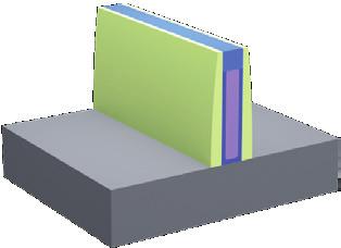
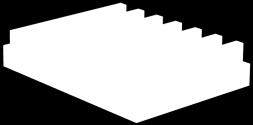
6 Patterning Inflection 100 nm Challenges Key Requirements Litho-Only Patterning Double Patterning Roughness CD varies Too much coverage Etch: Vertical and smooth profile Critical dimension (CD) uniformity High mask selectivity Repeatability Deposition: 100% step coverage with no pattern loading or voids Mechanically strong materials Repeatability Quadruple Patterning 25 nm Collapse Damage Clean : Collapse-free drying Particle removal without damage Particle 6

 architecture Low")


7 Patterning Inflection Growth Opportunity 7 Etch Dep Clean Differentiation Strategies Symmetric chamber, proprietary wafer temperature control Optimized process/hardware combinations Multi-station sequential deposition (MSSD) architecture Low surface tension chemistry Active Jet Technology Technology Adjacencies Leverage Σ N O V E L AM L U S Superior CD control, profile, repeatability Reduced line edge roughness and CD non-uniformity Repeatability, low cost of ownership Collapse-free drying Defect removal without damage Develop alternative films that are selective to etch and removable with wet etch Optimize deposition, etch, and trim to provide final desired mask profile and CD # Multiple Patterning Steps Opportunity NAND DRAM 5 Logic 0 N N+1 N+2 N = 28 nm Logic, 3x DRAM, ~20 nm NAND


8 FinFET Inflection ~10 nm Challenges Damage Residue Key Requirements Etch: No residue or structural damage Vertical profiles CD uniformity ~30 nm Void Deposition: Metal gates with no voids Repeatable, conformal spacer films Low resistivity, thin diffusion barriers Silicon loss Collapse Clean and Strip: Collapse-free drying No pattern damage No silicon loss 8

9 FinFET Inflection Growth Opportunity Etch Dep Clean Differentiation Strategies Proprietary technology to control ions and neutrals Proprietary wafer temperature control Dep-etch process Designer chemicals New barrier films Low surface tension chemistry Proprietary technologies Residue-free etching without structural damage Superior CD control, profile, and repeatability Void-free tungsten fill Highly conformal films Low resistivity diffusion barriers Collapse-free drying Defect removal without damage SAM Opportunity Flat to 10% growth in SAM for each 10k WSPM new capacity* Strip Non-oxidizing chemistry with low defectivity Metal gate integrity, ultra-low silicon loss 9 Technology Adjacencies Leverage Σ N O V E L AM L U S Optimize spacer properties by co-developing deposition and etch Optimize strip and clean together to minimize damage Planar Gate Process Flow FinFET Process Flow *Adjusted for productivity gains; excludes multiple patterning


10 3D NAND Inflection Challenges Key Requirements Holes not uniform 1,000 nm (= 1µm) Multi-Level Etch: High selectivity to hardmask Uniform holes in electrically active layers Defect Alternating film layers 10 Multi-Level Deposition: Alternating films without defects Repeatable films at high productivity Tungsten fill in complex geometry

11 3D NAND Inflection Growth Opportunity Differentiation Strategies SAM Opportunity Etch Advanced confined plasma technology Proprietary hardware/software Uniform holes through alternating films High selectivity to mask 35% 55% growth in SAM for each 10k WSPM new capacity* Optimized reactor geometry Films without defects Dep MSSD architecture Proprietary process High throughput density Tungsten fill without void Technology Adjacencies Leverage Σ N O V E L AM L U S Improve hardmask properties to enable etching of thicker stacks Tailor deposition of alternating films to improve etch profile Tune etch and clean to minimize residues without structural damage Planar NAND Process Flow 3D NAND Process Flow 11 *Adjusted for productivity gains


: Uniform backside thinning Thinning not uniform All")
12 Through-Silicon Via Inflection Challenges Key Requirements Scalloped sidewalls Etch: Smooth sidewalls Copper stud reveal without damage 50,000 nm (= 50 µm) TSV Voids Overburden Deposition: Copper fill with no voids Minimal copper overburden Repeatable copper fill Conformal liner and barrier Wafer Clean (Wet Etch): Uniform backside thinning Thinning not uniform All Products: High productivity 12

13 Through-Silicon Via Inflection Growth Opportunity Differentiation Strategies SAM Opportunity Etch Dep Advanced gas distribution with fast switching Exclusive chemistry, bath management Patented isotropic wet etch Smooth profiles at high throughput Void-free copper fill, repeatability Minimal copper overburden 70% - 120% growth in SAM* Novel liner and barrier Conformal films Clean Unique backside wet etch technology Uniform wafer thinning Technology Adjacencies Leverage Σ N O V E L AM L U S Optimize liner and barrier to enable increased etch productivity Optimize wet and dry etching to maximize productivity for copper stud reveal 2012 SAM 2015 SAM *Includes CMOS image sensor 13
14 Winning at the Inflections Technology inflections creating significant growth opportunities Winning strategies Identify the inflections: multiple patterning, FinFET, 3D NAND, TSV Create differentiation in each product offering: performance and productivity Leverage technology adjacencies Shipped market share objectives over the next 3-5 years: Etch (3-5%) 2300 Kiyo 2300 Flex 2300 Versys Metal 2300 Syndion Deposition (4-8%) VECTOR SPEED ALTUS SABRE SOLA Clean & Strip (5-10%) DV-Prime, Da Vinci 2300 Coronus GxT, G400, G3D 14
15 Panel Q&A Moderator: Rick Gottscho 15
16 Panel Participants Pat Lord Vice President and General Manager DGSI Product Group (Direct Metals, Gapfill, Surface Integrity, Integrated Metals) Joined Novellus in 2001 Ph.D. in Mechanical Engineering from the Massachusetts Institute of Technology 16

17 Panel Participants Mukund Srinivasan Vice President and General Manager Clean Product Group Joined Lam Research in 1996 Ph.D. in Mechanical Engineering from the University of California at Berkeley 17
18 Panel Participants Vahid Vahedi Vice President and General Manager Etch Product Group Joined Lam Research in 1995 Ph.D. in Electrical Engineering and Computer Science, from the University of California at Berkeley 18
19 Panel Participants Sesha Varadarajan Vice President and General Manager PECVD & Electrofill Product Group Joined Novellus in 1999 Masters Degree in Material Science from Boston University 19


20 Panel Participants Sesha Varadarajan Vahid Vahedi Mukund Srinivasan Pat Lord Rick Gottscho PECVD & Electrofill Etch Clean DGSI Moderator 20


21 21