Future electronics: Photonics and plasmonics at the nanoscale
|
|
|
- Laurence Griffith
- 5 years ago
- Views:
Transcription


1 Future electronics: Photonics and plasmonics at the nanoscale Robert Magnusson Texas Instruments Distinguished University Chair in Nanoelectronics Professor of Electrical Engineering Department of Electrical Engineering University of Texas-Arlington Arlington, Texas Applied Power Electronics Conference Fort Worth, Texas March 16 20,

2 Scope Plasmonics: Surface plasmons are coherent electron oscillations at the interface between two materials where the real part of the dielectric function changes sign across the interface. Nanoplasmonics: Plasmonics in nanoscale systems. Photonics: Technology concerned with the properties and transmission of photons, for example in fiber optics, waveguides, and lasers. Nanophotonics the study of the behavior of light on a nanometer scale. Engineering the interaction of light with particles or substances at deeply subwavelength scales. Silicon photonics: CMOS! Focus: Nanophotonic and nanoplasmonic periodic devices. 2


3 Nanoplasmonics Surface plasmons on dielectric-metal boundaries 3

4 Metal coupler example Jesse Lu, Csaba Petre, Eli Yablonovitch, and Josh Conway, Numerical optimization of a grating coupler for the efficient excitation of surface plasmons at an Ag SiO2 interface, J. Opt. Soc. Am. B/Vol. 24, No. 9/September
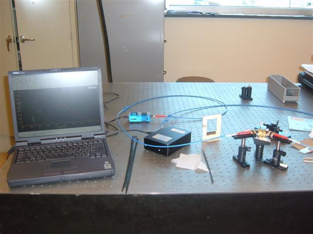
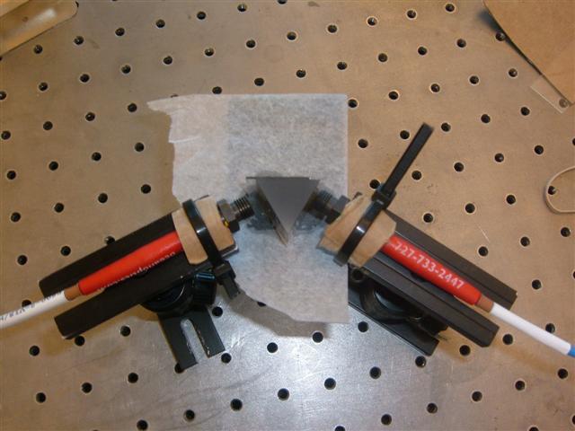
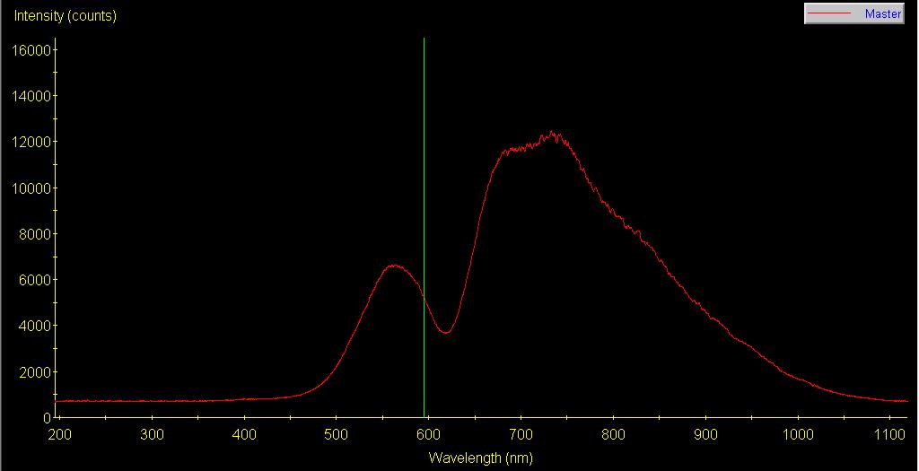
5 Undergrad plasmonics: SPR sensor experiment 5

6 SP-highlights Surface plasmon: EM field charge-density oscillation at the interface between a conductor and a dielectric SP: AC current at optical frequency Metallic structures: Concentrate/focus/guide light via SPs SP localization: Better than with dielectric optical means Efficient coupling/manipulation: Under intensive research Plasmonics: An electronics/photonics interface Our interest: Interaction/generation of plasmonic states employing leaky-mode resonance effects Fundamental plasmonic research in periodic nanostructures Theory and experiment in all cases 6
 Longitudinal surface wave in metal films Can be highly confined in nanostructures (localized plasmon) Propagates along the interface: few µm")
7 Surface plasmons-key properties Collective excitation of the free electrons in a metal Can be excited by light: photon-electron coupling (polariton)=spp Thin metal films or metal nanoparticles Bound to the interface (exponentially decaying along the normal) Longitudinal surface wave in metal films Can be highly confined in nanostructures (localized plasmon) Propagates along the interface: few µm to several mm (long range plasmon) Note: SP is a TM wave! 7


 and")


8 Model Device: Canonical periodic element Tranmission and modal properties air ε metal air H inc E inc FΛ Device possesses mixed cavitymodal (CM) and surfaceplasmon states (SPP) => EOT=extraordinary transmission Λ d Fixed Parameters ε metal = -5, F = 0.05 Yiwu Ding, Jaewoong Yoon, Muhammad H. Javed, Seok Ho Song, and Robert Magnusson, Mapping surface-plasmon polaritons and cavity modes in extraordinary optical transmission, IEEE Photonics Journal, vol. 3, no. 3, pp , June


9 Parametric Map of transmission function EOT 1.0 pure SPP region 0.8 mixed SPP/CM region d/λ= Λ/λ 0.4 TM 0 TM 1 TM 2 TM 3 TM 4 TM 5 TM 6 TM even mode odd mode higher order SPP d/λ cavity mode (CM) region 9


10 Mixed SPP-CM Region magnetic field patterns on TM 2 curve Gradual increase of surface field enhancement associated with SPP excitation Abrupt change in Fabry-Perot condition Missing resonance peaks 0.8 Λ/λ d/λ 10
 air I R 0 (b) 1.0 0.8 0.6 TM d FΛ Au Λ R 0 0.4 0.2 0.")
 (c) 20 (d) 15 15 10 10 5 5 d = 100 nm, λ = 710.")


11 Leaky modes and plasmons: Hybrid resonance elements (a) dielectric (n = 1.6) air I R 0 (b) TM d FΛ Au Λ R d=0 d=100nm d=900nm wavelength (µm) F=0.4 (fixed) (c) 20 (d) d = 100 nm, λ = nm 0 d = 900 nm, λ = nm 0 Robert Magnusson, Halldor Svavarsson, Jae Woong Yoon, Mehrdad Shokooh-Saremi, and Seok-Ho Song, Experimental observation of leaky modes and plasmons in a hybrid resonance element, Applied Physics Letters, vol. 100, no. 9, pp , February 29,
 air PR SPP 20 10 1.0 0.8 0.")

 TE 0 8 0 10 0.6 0.4 TE 0 (725 nm) 5 0.")
 Parameters: Λ = 653 nm, d PR =")
12 Measured spectra-computed fields PR silicon Au 500 nm (a) air PR SPP TM calculated measured Au Si (b) TM R TE TM 1 (669 nm) SPP (799 nm) calculated measured (c) TE TE 0 (725 nm) wavelength (µm) Parameters: Λ = 653 nm, d PR = 560 nm, d Au = 80 nm, n = 1.6, and F = Appl. Phys. Lett

13 Silicon photonics: Intel vision 13

14 Motivation for silicon photonics Limits of microelectronics evolution Optical communication evolution Interconnection bottlenecks Compact, low loss, EMI properties SiPhot=new technology platform Low cost High performance 14

15 Reference: Silicon Photonics PhD course prepared within FP Helios project 15

16 Huge opportunities for innovation! Reference: Silicon Photonics PhD course prepared within FP Helios project 16

17 Basic resonance interactions Excitation of a leaky eigenmode in 1D periodic layers Higher-order diffraction regime Zero-order diffraction regime Properties of 2D nanopatterns similar in principle 17

 1 0.9 0.8 1 0.")
 0 0.78 0.")
18 Experimental spectra Theory Experiment Reflectance Transmittance TE TM Wavelength (nm) Wavelength (nm) Simulation Experiment Transmittance Transmittance Simulated Measured λ (µm) Wavelength(µm) 18

, Photonic Integration: Integrated Optics: Devices,")
19 Guided-mode resonance nanophotonics: Innovation/applications platform Known knowns Unknown unknowns Interesting physics/properties Complex, interacting resonant leaky modes 1D or 2D periodic layers Applicable to dielectrics, semiconductors, metals Applicable to photonic, THz, microwave spectral regions Remaining challenges in analysis Remaining challenges in fabrication Many potential application fields Applications emerging ~Biosensors Favorable area for R&D&A R. Magnusson et al., Extraordinary capabilities of optical devices incorporating guided-mode resonance gratings, Optoelectronic Devices and Materials (OPTO), Photonic Integration: Integrated Optics: Devices, Materials, and Technologies XVIII, SPIE Photonics West 2014, San Francisco, California, February 1 6,
20 Guided-mode resonance technology: Application summary Frequency selective elements - Narrowband bandstop/bandpass filters ( λ~sub nm) - Wavelength division multiplexing (WDM) - Ultra high-q thin-film resonators - Laser resonator frequency selective mirrors Biochemical sensors - Spectroscopic biosensors - Chemical and environmental sensors - Multiparametric biosensors (biolayer thickness, refractive index, and background in a single measurement) Wideband lossless mirrors - Wideband bandstop/bandpass filters ( λ~100 s nm) - Mirrors for vertical-cavity lasers - Omnidirectional reflectors Polarization control elements - Polarization independent reflection/transmission elements for both 1D and 2D periodicity - Narrow or wideband polarizers - Non-Brewster polarizing laser mirrors - Polarization control including wave plates 20

21 Guided-mode resonance technology: Application summary Tunable elements - Tunable filters, EO modulators, and switches - Liquid-crystal integrated tunable devices - Laser cavity tuning elements - MEMS-tunable display pixels and filters - Thermally tuned silicon filters Security devices - Resonant Raman templates - Compact non-dispersive spectroscopy Thin-film light absorbers - Absorbance-enhanced solar cells - Omnidirectional, wideband, polarization-independent absorbers - GMR coherent perfect absorbers Photonic metasurfaces - Wavefront-shaping elements including focusing reflectors Dispersive elements - Slow-light/dispersion elements Hybrid resonant elements - Leaky-mode nanoplasmonics - Hybrid plasmonic/modal resonance sensors - Rayleigh reflectors with sharp angular cutoff - Rayleigh-anomaly based GMR transmission filters 21
 Model and reflectance/transmittance spectra of a GMR mirror applying a partially etched Ge layer. Input light is in a TM polarization state. R. Magnusson et al.")
22 Wideband resonant reflectors 1.0 d g d h z Λ FΛ y x R 0 Ge SiO 2 air zero-order efficiency BW~900 nm R 0 T 0 T wavelength (µm) Model and reflectance/transmittance spectra of a GMR mirror applying a partially etched Ge layer. Input light is in a TM polarization state. R. Magnusson et al., Extraordinary capabilities of optical devices incorporating guided-mode resonance gratings, Optoelectronic Devices and Materials (OPTO), Photonic Integration: Integrated Optics: Devices, Materials, and Technologies XVIII, SPIE Photonics West 2014, San Francisco, California, February 1 6,


23 Color filter array: Design Designed and optimized with RCWA Parameters: n = 2.02, F = 0.5, d g = 55 nm, and d h = 110 nm. Period-tuned resonance wavelengths enabling RGB color filters. Mohammad J. Uddin and Robert Magnusson, Highly efficient color filter array using resonant Si 3 N 4 gratings, Optics Express, vol. 21, no. 10, pp , May 20,
24 Results: Spectral measurements Device Parameters: d g = 60 nm, d h 105 nm, F = High experimental efficiency (> 95%) with low crosstalk Mohammad J. Uddin and Robert Magnusson, Highly efficient color filter array using resonant Si 3 N 4 gratings, Optics Express, vol. 21, no. 10, pp , May 20,


25 Label-free Microarrays Based on Guided-mode Resonance Technology Products Fully automated benchtop reader 96-well and 384-well disposable label-free microarray plates Pre-sensitized kits: standard and custom Comprehensive assay support for transition to label-free Features Optical resonance with real-time data Cell-based and biochemical assays Dual-resonance detection enables two data points for every measurement Multiplexing capability ResonantSensors.com

26 Conclusions Nanoplasmonics Light on metals-compact devices Loss/gain compromise Rapid R&D Silicon photonics CMOS infrastructure Integrated electronics/photonics chips Commercial now Under intense development Nanophotonics Device development opportunities Opportunities in entrepreneurship/innovation 26