The 3D Silicon Leader
|
|
|
- Steven Watson
- 6 years ago
- Views:
Transcription

1 The 3D Silicon Leader TSV technology embedding high density capacitors for advanced 3D packaging solutions IMAPS Device Packaging Conference 2014 Catherine Bunel
2 Outline Introduction IPDiA s unique Capacitor technology TSV + passives Examples of 3D integration Performances Conclusion 2
3 Who are we?


4 Who are we? Independent Company located in Caen, Normandy, France Dedicated to manufacturing of leading edge Integrated Passive Devices Operating own Silicon wafer fab Strong R&D team and collaborations with leading research institutes 4


5 IPDiA: Turnkey Supplier One-Stop-Shop for the Integrated Passive Devices Pre-studies & Design Center Foundry Services Mid-end Services Assembly Services From your schematics, we design and manufacture High Quality Products 5

 OHSAS-18001 RoHS compliant AEO (Authorised")
6 Industrial partner IPDIA manufactures Semiconductor based products and is organized to support High Tech companies ISO-9001 ISO ISO-TS16949 (Automotive) ISO (Medical) OHSAS RoHS compliant AEO (Authorised Economic Operator) 6
7 IPDiA s unique Capacitor technology

8 IPDiA s unique Capacitor Technology 8

9 Capacitor Integration Density Qualified for volume manufacturing 14/03/2014 9


10 3D structure Surface Gain Surface gain versus pillar depth and geometry Pillars depth (µm) 10
11 3D structure 2 parallelized capacitors in a MIMIM architecture in order to increase the capacitance value Simplified MIMIM architecture from the PICS3 Related schematic Middle electrode (in-situ doped Polysilicon1) Top electrode (in-situ doped Polysilicon2) Passivation layer (SiO 2 ) Bottom electrode (N++ area) Metal layers Polysilicon 1 (PS1) Polysilicon2 Dielectric2 Polysilicon1 Dielectric1 N++ Area Low Ohmic substrate P+, 20 Silicon mohm.cm substrate PS1 PS1 Dielectric 2 Dielectric 1 PS2 N++ Metal layers

12 3D structure Capacitor stack is based on highly engineered high-k materials X Z Y Z Y Z Y Z Y Z Y X Y-Z X X 23/04/10 Florent LALLEMAND 12
13 Performances Breakdown voltage > 10V Low leakage current <1nA/mm² Excellent temperature and voltage linearity < 100ppm/ K & < 100ppm/V Silicon capacitors and arrays are insensitive to operating temperatures between 65 C to 250 C Excellent matching < 2% High reliability > 10 operating 100 C FIT (Failure in Time) below 1 at 225 C Mechanical shock tests pass easily as well as thermal cycling tests (up to 3000 cycles in TMCL) Low ESR 14/03/2014 Florent LALLEMAND 13

14 Where are we? Low profile High reliability Medical implantables Non Magnetic High Temperature applications IC decoupling, Optical Networking, GaN based Power Amplifiers and DC/DC Converters Where Performiniaturization is required!!! 14

15 3D Capacitor Density Roadmap PICS4 500nF/mm² BV 11v PICS5 1µF/mm² BV 11v 250nF/mm² BV 11v PICS3 HV 100nF/mm² BV 30v PICS4 HV 200nF/mm² BV 30v 4µF/mm² BV 30v 20nF/mm² BV 50v 3µF/mm² BV 50v 5nF/mm² BV 150v 1.3nF/mm² BV 450v 700nF/mm² BV 100v Production Qualification R&D Florent LALLEMAND 15
16 TSV + Passives IPDiA s approach
17 TSV + passives : 3D IC with TSV is a key innovation enabling miniaturized electronic systems Customers see benefit in performance,power and footprint but they don t want to pay more Niche Extanded lifetime Simplification Killer applications are with passives or sensors 17
18 Via last approach Copper inductors MIM Capacitor Barrier Isolation Polysilicon Resistor Copper High Density Capacitor High Ohmic Substrate NiAu UBM + CUSn Bumps 18 Passivation
19 TSV features Design Factors Value Silicon wafer resistivity 1 kώ-cm TSV depth 200µm TSV diameter 75µm TSV pitch 125µm Keep out area 15µm Silicon dioxide liner thickness 1.5µm 2 metal layers 1µm Al & 6µm Cu RDL Cu 3µm Vias filling Cu partial or complete filling passivation Epoxy based 9µm Under bump metallization NiAu electroless 5µm Solder bump diameter 70µm 19
20 TSV performances Designation Insulation breakdown voltage > 200v Serial resistivity per via < 10mOhms Serial inductor per via Via to via capacitance Insertion loss Coupling to substrate <100pH < 1pF 20GHz
21 TSV + Passives Examples of application Florent LALLEMAND
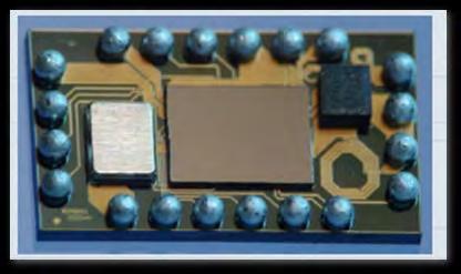
22 TSV + passives : example 1 transceiver Crystal SAW IPD Benefits : Miniaturization thanks to the high capacitor density Performances Reliability Cost Module Size : 10mm * 7mm * 1,2mm Passives : High density capacitors for decoupling,rf MIM capacitors, resistors, matching network, band-pass filter. Active components on top of the IPD : Saw filter,microcrystal, RF transceiver Cu RDL,NiAu UBM, SnPb solder balls,soldering on PCB 22
23 TSV + passives : example 1 transceiver Crystal SAW IPD Status : First time right with a Yield of 65% ( yield loss root causes identified) Fully functional in the application Reliability tests passed successfully : Temperature cycling (TMCL) -40C <-> +125C, 10 cycles HTSL test (thermo shock) +150C, 24h 0 fails ESD : HBM 750V, MM 100V, CDM 400V 23


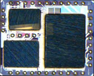
24 TSV + passives : example 2 Module Size : 6 mm * 10mm * 3 mm Passives : high density capacitors, MIM capacitors, High value resistances. Cu RDL,NiAu UBM Active components on top of the IPD : Amplifier, switches, smd, PICS Capacitors Molded in a package and soldered on PCB 24
25 TSV + passives : example 2 Benefits : Miniaturization thanks to the high integration ( High Voltage Capacitor 100nF/mm², High Stability Resistors 800kOhms/sq, highly integrated package, volume & weight reduction) Cost reduction of 40% Excellent matching < 2% for the passives High stability Reliability >10 15v,125 C EMPC 2013 : 3D TSV System in Package (SiP) for aerospace applications Safran, IPDiA 25

26 Electrical test Wafer probe test before TSV making TSV continuity thanks to dedicated structures XRay analysis Electrical test on final module 26
27 Conclusion IPDiA continues its commitment to provide 3D/TSV technology with IPD to optimize system integration solutions for best performances (speed/power,stability,reliability), lowest cost, and smallest form factor Feasability was demonstrated on several demonstrators Qualification under medical conditions and reliable manufacturability of IPDiA TSV technology was proven will be the year of 3D!!! (SEMI European 3D TSV Summit) 27
28 Acknowledgments The authors would like to thank : Our Research partners from The members of for sponsoring this work included in the PRIIM project. 28

29 Thank you for attention!

30 30
High performance and high reliability passives for miniature medical devices based upon Silicon technologies. Laurent Dubos INEMI May 2011
 High performance and high reliability passives for miniature medical devices based upon Silicon technologies Laurent Dubos INEMI May 2011 IPDIA overview Company located in Caen, Normandy, France Started
Silicon Interposers with Integrated Passive Devices: Ultra-Miniaturized Solution using 2.5D Packaging Platform
 Minapad 2014, May 21 22th, Grenoble; France Silicon Interposers with Integrated Passive Devices: Ultra-Miniaturized Solution using 2.5D Packaging Platform Stéphane Bellenger, Laëtitia Omnès, Jean-René
The 3D Silicon Leader. Company Presentation. SMTA Houston, 14th March 2013
 The 3D Silicon Leader Company Presentation SMTA Houston, 14th March 2013 Who are we? Independent Company located in Caen, Normandy, France Dedicated to manufacturing of leading edge Integrated Passive
ASPICS IPD Companion for ISM Transceiver IC: RF front end part
 IPD Companion for ISM Transceiver IC: RF front end part Rev 1.2 TD Introduction The ASPICS320.606 is an integrated passives device specifically designed for use with the SEMTECH SX1211 868/915MHz ISM/UHF
RF System in Packages using Integrated Passive Devices
 RF System in Packages using Integrated Passive Devices by Kai Liu, YongTaek Lee, HyunTai Kim, Gwang Kim, and Billy Ahn STATS ChipPAC 1711 W. Greentree Drive, Suite #117, Tempe, AZ 85284, USA Tel: 480-222-1722
WIRE BOND CAPACITORS, RESISTORS & INTEGRATED PASSIVE COMPONENTS FOR CHIP & WIRE ASSEMBLY
 WIRE BOND CAPACITORS, RESISTORS & INTEGRATED PASSIVE COMPONENTS FOR CHIP & WIRE ASSEMBLY ABOUT AVX COMPANY INFORMATION AVX is a leading international manufacturer and supplier of a vast portfolio of advanced
Development and Characterization of 300mm Large Panel ewlb (embedded Wafer Level BGA)
") Development and Characterization of 300mm Large Panel ewlb (embedded Wafer Level BGA) Seung Wook Yoon, Yaojian Lin and Pandi C. Marimuthu STATS ChipPAC Ltd. 5 Yishun Street 23, Singapore 768442 E-mail
Development and Characterization of 300mm Large Panel ewlb (embedded Wafer Level BGA) Seung Wook Yoon, Yaojian Lin and Pandi C. Marimuthu STATS ChipPAC Ltd. 5 Yishun Street 23, Singapore 768442 E-mail
WBSC Wire Bonding vertical Silicon Capacitor
 WBSC Wire Bonding vertical Silicon Capacitor Rev 4.0 Key Features Key Applications Wire bondable vertical capacitors Physical parameters: - Various sizes: from 0101 to 0805 format - Substrate: Silicon
ASPICS /5 IPD Companion for ISM Transceiver IC: Synthesis part
 ASPICS320.604/5 IPD Companion for ISM Transceiver IC: Synthesis part Rev 1.2 TD General description Features The ASPICS320.604/605 are integrated passive devices specifically designed for use with the
Low Temperature Co-fired Ceramics (LTCC) Multi-layer Module Boards
 Multi-layer Module Boards") Low Temperature Co-fired Ceramics () Multi-layer Module Boards Example: Automotive Application Example: Communication Application Murata's Low Temperature Co-fired Ceramics offer highly integrated substrates
Low Temperature Co-fired Ceramics () Multi-layer Module Boards Example: Automotive Application Example: Communication Application Murata's Low Temperature Co-fired Ceramics offer highly integrated substrates
Narrowing the Gap between Packaging and System
 Narrowing the Gap between Packaging and System Meptec Symposium 2015 ASE (US) Inc Ou Li Nov 10 th, 2015 Outline Industry Dynamics The Need for System Integrators IC/Pkg/System Collaboration Summary 2 Market
Chips Face-up Panelization Approach For Fan-out Packaging
 Chips Face-up Panelization Approach For Fan-out Packaging Oct. 15, 2015 B. Rogers, D. Sanchez, C. Bishop, C. Sandstrom, C. Scanlan, TOlson T. REV A Background on FOWLP Fan-Out Wafer Level Packaging o Chips
UBSC/ULSC 60 + GHz Ultra Broadband Silicon Capacitors Surface Mounted
 Rev 2.5 UBSC/ULSC 60 + GHz Ultra Broadband Silicon Capacitors Surface Mounted Key Features Ultra broadband performance up to 60 + GHz Resonance free Phase stability Ultra high stability of capacitance
Close supply chain collaboration enables easy implementation of chip embedded power SiP
 Close supply chain collaboration enables easy implementation of chip embedded power SiP Gerald Weidinger, R&D Project Leader, AT&S AT & S Austria Technologie & Systemtechnik Aktiengesellschaft Fabriksgasse13
3D Package Technologies Review with Gap Analysis for Mobile Application Requirements. Apr 22, 2014 STATS ChipPAC Japan
 3D Package Technologies Review with Gap Analysis for Mobile Application Requirements Apr 22, 2014 STATS ChipPAC Japan T.Nishio Contents Package trends and roadmap update Advanced technology update Fine
Mobile Device Passive Integration from Wafer Process
 Mobile Device Passive Integration from Wafer Process Kai Liu, YongTaek Lee, HyunTai Kim, and MaPhooPwint Hlaing STATS ChipPAC, Inc. 1711 West Greentree, Suite 117, Tempe, Arizona 85284, USA Tel: 48-222-17
Integration of Power-Supply Capacitors with Ultrahigh Density on Silicon Using Particulate Electrodes POWERSOC 2012
 Integration of Power-Supply Capacitors with Ultrahigh Density on Silicon Using Particulate Electrodes POWERSOC 2012 P M Raj, Himani Sharma, Kanika Sethi, Prof. Rao Tummala 3D Systems Packaging Research
Cost effective 300mm Large Scale ewlb (embedded Wafer Level BGA) Technology
 Technology") Cost effective 300mm Large Scale ewlb (embedded Wafer Level BGA) Technology by Meenakshi Prashant, Seung Wook Yoon, Yaojian LIN and Pandi C. Marimuthu STATS ChipPAC Ltd. 5 Yishun Street 23, Singapore 768442
Cost effective 300mm Large Scale ewlb (embedded Wafer Level BGA) Technology by Meenakshi Prashant, Seung Wook Yoon, Yaojian LIN and Pandi C. Marimuthu STATS ChipPAC Ltd. 5 Yishun Street 23, Singapore 768442
Fraunhofer IZM. All Silicon System Integration Dresden Scope. M. Juergen Wolf
 Fraunhofer IZM All Silicon System Integration Dresden Scope M. Juergen Wolf Fraunhofer IZM All Silicon System Integration - ASSID Dresden, Berlin, Germany Fraunhofer IZM Focus of Activities Materials,
3D-IC Integration using D2C or D2W Alignment Schemes together with Local Oxide Reduction
 3D-IC Integration using D2C or D2W Alignment Schemes together with Local Oxide Reduction Gilbert Lecarpentier*, Jean-Stéphane Mottet* SET S.A.S. (Smart Equipment Technology), 131 Impasse Barteudet, 74490
A LOW SERIES RESISTANCE, HIGH DENSITY, TRENCH CAPACITOR FOR HIGH-FREQUENCY APPLICATIONS
 A LOW SERIES RESISTANCE, HIGH DENSITY, TRENCH CAPACITOR FOR HIGH-FREQUENCY APPLICATIONS Gordon Grivna, Sudhama Shastri, Yujing Wu, & Will Cai Sept, 2008 www.onsemi.com Presentation Outline 1. Introduction
5. Packaging Technologies Trends
 5. Packaging Technologies Trends Electronic products and microsystems continue to find new applications in personal, healthcare, home, automotive, environmental and security systems. Advancements in packaging
Die Thickness Effects in RF Front-End Module Stack-Die Assemblies
 Die Thickness Effects in RF Front-End Module Stack-Die Assemblies By Kai Liu*, YongTaek Lee, HyunTai Kim, Gwang Kim, Robert Frye**, Hlaing Ma Phoo Pwint***, and Billy Ahn * STATS ChipPAC, Inc. 1711 West
Next Generation High-Q Compact Size IPD Diplexer for RF Frond End SiP
 2017 IEEE 67th Electronic Components and Technology Conference Next Generation High-Q Compact Size IPD Diplexer for RF Frond End SiP Sheng-Chi Hsieh, Pao-Nan Lee, Hsu-Chiang Shih, Chen-Chao Wang, Teck
System in Package: Identified Technology Needs from the 2004 inemi Roadmap
 System in Package: Identified Technology Needs from the 2004 inemi Roadmap James Mark Bird Amkor Technology Inc System in package (SiP) technology has grown significantly in the past several years. It
Welcome to the KEMET Ceramic Capacitor Flex Crack Mitigation product training module. This module will review sources of stress in surface mount
 1 Welcome to the KEMET Ceramic Capacitor Flex Crack Mitigation product training module. This module will review sources of stress in surface mount multilayer ceramic capacitors, provide board layout recommendations,
Electrical and Fluidic Microbumps and Interconnects for 3D-IC and Silicon Interposer
 Electrical and Fluidic Microbumps and Interconnects for 3D-IC and Silicon Interposer Li Zheng, Student Member, IEEE, and Muhannad S. Bakir, Senior Member, IEEE Georgia Institute of Technology Atlanta,
Embedded Passives..con0nued
 Embedded Passives..con0nued Why Embedded Passives? Improves the packaging efficiency System-on-Package (SOP); SLIM integration Reducing size Eliminating substrate assembly Minimizing solder joint failure
YOUR Strategic TESTING ENGINEERING CONCEPT SMT FLIP CHIP PRODUCTION OPTO PACKAGING PROCESS DEVELOPMENT CHIP ON BOARD SUPPLY CHAIN MANAGEMENT
 YOUR Strategic TECHNOLOGY PARTNER Wafer Back-End OPTO PACKAGING PROCESS DEVELOPMENT CONCEPT FLIP CHIP PROTOTYping ENGINEERING TESTING SMT PRODUCTION CHIP ON BOARD SUPPLY CHAIN MANAGEMENT Next Level 0f
TSV Interposer Process Flow with IME 300mm Facilities
 TSV Interposer Process Flow with IME 300mm Facilities Property of Institute of Microelectronics (IME)-Singapore August 17, 2012 Outline 1. TSV interposer (TSI) cross sectional schematic TSI with BEOL,
YOUR Strategic TESTING ENGINEERING CONCEPT SMT FLIP CHIP PRODUCTION OPTO PACKAGING PROCESS DEVELOPMENT CHIP ON BOARD SUPPLY CHAIN MANAGEMENT
 YOUR Strategic TECHNOLOGY PARTNER Wafer Back-End OPTO PACKAGING PROCESS DEVELOPMENT CONCEPT FLIP CHIP PROTOTYping ENGINEERING TESTING SMT PRODUCTION CHIP ON BOARD SUPPLY CHAIN MANAGEMENT Next Level 0f
Passive component embedding in printed circuit boards for space applications
 Passive component embedding in printed circuit boards for space applications 2nd Space Passive Component Days (SPCD), International Symposium 12-14 October 2016 ESA/ESTEC, Noordwijk, The Netherlands Maarten
ATSC Automotive Grade Silicon Capacitors
 ATSC Automotive Grade Silicon Capacitors Rev 1.1 Key Features Qualified according to AEC-Q100 Ultra long life @ 200 C High stability of capacitance value: Temperature
CX Thin Fil s. Resistors Attenuators Thin-Film Products Thin-Film Services. ISO 9001:2008 RoHS/REACH Compliant ITAR Compliant
 CX Thin Fil s Resistors Attenuators Thin-Film Products Thin-Film Services www.cxthinfilms.com ISO 9001:2008 RoHS/REACH Compliant ITAR Compliant www.cxthinfilms.com sales@cxthinfilms.com +1 (401) 461-5500
New Component Technologies Enable More Robust and Reliable Power System Design
 New Component Technologies Enable More Robust and Reliable Power System Design APEC2016 Chris Reynolds Technical Marketing Manager AVX Corporation (843) 424 1209 AVX Corporation 2016 http://www.avx.com
ewlb (embedded Wafer Level BGA) Technology: Next Generation 3D Packaging Solutions
 Technology: Next Generation 3D Packaging Solutions") ewlb (embedded Wafer Level BGA) Technology: Next Generation 3D Packaging Solutions by Seung Wook Yoon and Meenakshi Padmanathan STATS ChipPAC Ltd. Seungwook.yoon@statschippac.com Andreas Bahr Infineon
ewlb (embedded Wafer Level BGA) Technology: Next Generation 3D Packaging Solutions by Seung Wook Yoon and Meenakshi Padmanathan STATS ChipPAC Ltd. Seungwook.yoon@statschippac.com Andreas Bahr Infineon
Chapter 4 Fabrication Process of Silicon Carrier and. Gold-Gold Thermocompression Bonding
 Chapter 4 Fabrication Process of Silicon Carrier and Gold-Gold Thermocompression Bonding 4.1 Introduction As mentioned in chapter 2, the MEMs carrier is designed to integrate the micro-machined inductor
Innovative Substrate Technologies in the Era of IoTs
 Innovative Substrate Technologies in the Era of IoTs Dyi- Chung Hu 胡迪群 September 4, 2015 Unimicron Contents Introduction Substrate Technology - Evolution Substrate Technology - Revolution Glass substrate
FLIP CHIP CHIP ON BOARD SMT ENGINEERING OPTO PACKAGING SUPPLY CHAIN MANAGEMENT TESTING YOUR INNOVATIVE TECHNOLOGY PARTNER PRODUCTION CONCEPT
 YOUR INNOVATIVE TECHNOLOGY PARTNER CHIP ON BOARD OPTO PACKAGING PROCESS DEVELOPMENT CONCEPT FLIP CHIP ENGINEERING TESTING PRODUCTION SMT SUPPLY CHAIN MANAGEMENT PROTOTYPES HIGH-PRECISION ASSEMBLY OF MICRO-
Fan-Out Packaging Technologies and Markets Jérôme Azémar
 Fan-Out Packaging Technologies and Markets Jérôme Azémar Senior Market and Technology Analyst at Yole Développement Outline Advanced Packaging Platforms & Market drivers Fan-Out Packaging Principle & Definition
FRAUNHOFER INSTITUTE FOR RELIABILITY AND MICROINTEGRATION IZM DEPARTMENT WAFER LEVEL SYSTEM INTEGRATION BERLIN
 FRAUNHOFER INSTITUTE FOR RELIABILITY AND MICROINTEGRATION IZM DEPARTMENT WAFER LEVEL SYSTEM INTEGRATION BERLIN WAFER LEVEL SYSTEM INTEGRATION ELECTRONIC PACKAGING AT FRAUNHOFER IZM The Fraunhofer Institute
Introducing KEMET Tantalum Low DC Leakage MnO2 Series. One WORLD One Brand One Strategy One Focus One Team One KEMET
 Introducing KEMET Tantalum Low DC Leakage MnO2 Series One WORLD One Brand One Strategy One Focus One Team One KEMET Purpose Introduce KEMET s Low DC Leakage MnO2 Series () Objectives Define the features
FRAUNHOFER INSTITUTE FOR RELIABILITY AND MICROINTEGRATION IZM DEPARTMENT WAFER LEVEL SYSTEM INTEGRATION BERLIN
 FRAUNHOFER INSTITUTE FOR RELIABILITY AND MICROINTEGRATION IZM DEPARTMENT WAFER LEVEL SYSTEM INTEGRATION BERLIN WAFER LEVEL SYSTEM INTEGRATION ELECTRONIC PACKAGING AT FRAUNHOFER IZM The Fraunhofer Institute
Challenges and Solutions for Cost Effective Next Generation Advanced Packaging. H.P. Wirtz, Ph.D. MiNaPAD Conference, Grenoble April 2012
 Challenges and Solutions for Cost Effective Next Generation Advanced Packaging H.P. Wirtz, Ph.D. MiNaPAD Conference, Grenoble April 2012 Outline Next Generation Package Requirements ewlb (Fan-Out Wafer
Roundtable 3DIC & TSV: Ready for HVM? European 3D TSV Summit
 Roundtable 3DIC & TSV: Ready for HVM? European 3D TSV Summit Infineon VTI Xilinx Synopsys Micron CEA LETI 2013 Yann Guillou Business Development Manager Lionel Cadix Market & Technology Analyst, Advanced
FOR SEMICONDUCTORS 2009 EDITION
 INTERNATIONAL TECHNOLOGY ROADMAP FOR SEMICONDUCTORS 2009 EDITION INTERCONNECT THE ITRS IS DEVISED AND INTENDED FOR TECHNOLOGY ASSESSMENT ONLY AND IS WITHOUT REGARD TO ANY COMMERCIAL CONSIDERATIONS PERTAINING
Thales vision & needs in advanced packaging for high end applications
 Thales vision & needs in advanced packaging for high end applications M. Brizoux, A. Lecavelier Thales Global Services / Group Industry Chemnitzer Seminar June 23 th -24 th, 2015 Fraunhofer ENAS - Packaging
EE 434 Lecture 9. IC Fabrication Technology
 EE 434 Lecture 9 IC Fabrication Technology Quiz 7 The layout of a film resistor with electrodes A and B is shown. If the sheet resistance of the film is 40 /, determine the resistance between nodes A and
JOINT INDUSTRY STANDARD
 JOINT INDUSTRY STANDARD AUGUST 1999 Semiconductor Design Standard for Flip Chip Applications ASSOCIATION CONNECTING ELECTRONICS INDUSTRIES Semiconductor Design Standard for Flip Chip Applications About
Fairchild Semiconductor Application Note June 1983 Revised March 2003
 Fairchild Semiconductor Application Note June 1983 Revised March 2003 High-Speed CMOS (MM74HC) Processing The MM74HC logic family achieves its high speed by utilizing microcmos Technology. This is a 3.5
Considerations for Embedding Passives and Actives in PCBs
 Considerations for Embedding Passives and Actives in PCBs PwrSoC 2014 AT & S Austria Technologie & Systemtechnik Aktiengesellschaft Fabriksgasse 13 A-8700 Leoben Tel +43 (0) 3842 200-0 E-mail info@ats.net
System-in-Package (SiP) on Wafer Level, Enabled by Fan-Out WLP (ewlb)
 on Wafer Level, Enabled by Fan-Out WLP (ewlb)") System-in-Package (SiP) on Wafer Level, Enabled by Fan-Out WLP (ewlb) Steffen Kröhnert, José Campos, Eoin O Toole NANIUM S.A., Vila do Conde, Portugal Outline Short Company Overview NANIUM Introduction
System-in-Package (SiP) on Wafer Level, Enabled by Fan-Out WLP (ewlb) Steffen Kröhnert, José Campos, Eoin O Toole NANIUM S.A., Vila do Conde, Portugal Outline Short Company Overview NANIUM Introduction
IME Proprietary. EPRC 12 Project Proposal. 3D Embedded WLP. 15 th August 2012
 EPRC 12 Project Proposal 3D Embedded WLP 15 th August 2012 Motivation Factors driving IC market Higher density, lower cost, high yield Fan-out WLP/eWLP advantages Small footprint, low profile Low cost,
By Ron Blankenhorn, Pac Tech USA, Santa Clara, Calif., and Thomas Oppert, Pac Tech GbmH, Nauen, Germany
 INTRODUCTION Modern microelectronic products require packages that address the driving forces of reduced size and weight, as well as increased performance at high frequencies. Flipchip and direct chip
Research Needs: Packaging June 25, 2018 Semiconductor Research Corp. (SRC) Research Triangle Park, NC 27703
 Research Triangle Park, NC 27703") Research Needs: Packaging June 25, 2018 Semiconductor Research Corp. (SRC) Research Triangle Park, NC 27703 Background Semiconductor- based computing has revolutionized all aspects of modern life and will
Research Needs: Packaging June 25, 2018 Semiconductor Research Corp. (SRC) Research Triangle Park, NC 27703 Background Semiconductor- based computing has revolutionized all aspects of modern life and will
IMPLEMENTATION OF A FULLY MOLDED FAN-OUT PACKAGING TECHNOLOGY
 IMPLEMENTATION OF A FULLY MOLDED FAN-OUT PACKAGING TECHNOLOGY B. Rogers, C. Scanlan, and T. Olson Deca Technologies, Inc. Tempe, AZ USA boyd.rogers@decatechnologies.com ABSTRACT Fan-Out Wafer-Level Packaging
Cu electroplating in advanced packaging
 Cu electroplating in advanced packaging March 12 2019 Richard Hollman PhD Principal Process Engineer Internal Use Only Advancements in package technology The role of electroplating Examples: 4 challenging
SLIM TM, High Density Wafer Level Fan-out Package Development with Submicron RDL
 2017 IEEE 67th Electronic Components and Technology Conference SLIM TM, High Density Wafer Level Fan-out Package Development with Submicron RDL YoungRae Kim 1, JaeHun Bae 1, MinHwa Chang 1, AhRa Jo 1,
Ultra Fine Pitch Bumping Using e-ni/au and Sn Lift-Off Processes
 Ultra Fine Pitch Bumping Using e-ni/au and Sn Lift-Off Processes Andrew Strandjord, Thorsten Teutsch, and Jing Li Pac Tech USA Packaging Technologies, Inc. Santa Clara, CA USA 95050 Thomas Oppert, and
Maxim Integrated Global Failure Analysis (FA)
") Maxim Integrated Global Failure Analysis (FA) Vision Empower industry leading technologies, protect product brand promises, and be the competitive advantage for Maxim Integrated. Mission Deliver timely,
Maxim Integrated Global Failure Analysis (FA) Vision Empower industry leading technologies, protect product brand promises, and be the competitive advantage for Maxim Integrated. Mission Deliver timely,
9 rue Alfred Kastler - BP Nantes Cedex 3 - France Phone : +33 (0) website :
 website :") 9 rue Alfred Kastler - BP 10748-44307 Nantes Cedex 3 - France Phone : +33 (0) 240 180 916 - email : info@systemplus.fr - website : www.systemplus.fr February 2012 - Version 1 Written by: Romain FRAUX DISCLAIMER
9 rue Alfred Kastler - BP 10748-44307 Nantes Cedex 3 - France Phone : +33 (0) 240 180 916 - email : info@systemplus.fr - website : www.systemplus.fr February 2012 - Version 1 Written by: Romain FRAUX DISCLAIMER
LTCC SYSTEMS and LTCC DESIGN RULES
 LTCC SYSTEMS and LTCC DESIGN RULES Low Temperature Co-fired Ceramic revision status: G page 1 of 19 Table of Contents: 1 General page 3 2 Commercial LTCC tape systems page 4 3 Design possibilities page
Metal Composite Type Power Choke Coils
 ETQ-PM Series Inductor Product Guide Metal Composite Type Power Choke Coils AEC-Q200 Compliant For Use In Harsh Environments Vibration Resistance of 10G ~ 30G (5Hz 2kHz) Maximum Operating Temperature of
A Flexible Vertical MEMs Probe Card Technology for Pre-Bump and ewlp Applications
 June 12 to 15, 2011 San Diego, CA A Flexible Vertical MEMs Probe Card Technology for Pre-Bump and ewlp Applications Mike Slessor Rick Marshall (MicroProbe, Inc.) Vertical MEMS for Pre-Bump Probe Introduction:
TGV and Integrated Electronics
 TGV and Integrated Electronics Shin Takahashi ASAHI GLASS CO., LTD. 1 Ambient Intelligence Green Energy/Environment Smart Factory Smart Mobility Smart Mobile Devices Bio/Medical Security/Biometrics 2 Glass
28nm Mobile SoC Copper Pillar Probing Study. Jose Horas (Intel Mobile Communications) Amy Leong (MicroProbe) Darko Hulic (Nikad)
 Amy Leong (MicroProbe) Darko Hulic (Nikad)") 28nm Mobile SoC Copper Pillar Probing Study Jose Horas (Intel Mobile Communications) Amy Leong (MicroProbe) Darko Hulic (Nikad) Overview Introduction to IMC Copper Pillar Implementation at IMC Low force
28nm Mobile SoC Copper Pillar Probing Study Jose Horas (Intel Mobile Communications) Amy Leong (MicroProbe) Darko Hulic (Nikad) Overview Introduction to IMC Copper Pillar Implementation at IMC Low force
Flip Chip Bump Electromigration Reliability: A comparison of Cu Pillar, High Pb, SnAg, and SnPb Bump Structures
 Flip Chip Bump Electromigration Reliability: A comparison of Cu Pillar,,, and SnPb Bump Structures Ahmer Syed, Karthikeyan Dhandapani, Lou Nicholls, Robert Moody, CJ Berry, and Robert Darveaux Amkor Technology
Chapter 3 Silicon Device Fabrication Technology
 Chapter 3 Silicon Device Fabrication Technology Over 10 15 transistors (or 100,000 for every person in the world) are manufactured every year. VLSI (Very Large Scale Integration) ULSI (Ultra Large Scale
2009 Technical Plan. TIG Chair: John Davignon T.C. / TIG Meeting Las Vegas, Nevada April 3, 2009
 2009 Technical Plan TIG Chair: John Davignon T.C. / TIG Meeting Las Vegas, Nevada April 3, 2009 Technical Plan Agenda Introduction What has changed Preliminary Gap Chart Preliminary Five-year plan Preliminary
Next Gen Packaging & Integration Panel
 Next Gen Packaging & Integration Panel ECTC 2012 Daniel Tracy, Sr. Director Industry Research & Statistics SEMI May 29, 2012 Packaging Supply Chain Market Trends Material Needs and Opportunities Market
Focus on Power: Advancements in Ceramic Capacitors. Topics. APEC 2011 Special Presentation MLCC Advancements in Ceramic Capacitors March 2011
 Focus on Power: Advancements in Ceramic Capacitors Michael Cannon Product Marketing Dept. 1 Topics 1. Materials Recent advances in material technology and design have allowed multilayer ceramic capacitors
EE 330 Lecture 9. IC Fabrication Technology Part II. -Oxidation -Epitaxy -Polysilicon -Planarization -Resistance and Capacitance in Interconnects
 EE 330 Lecture 9 IC Fabrication Technology Part II -Oxidation -Epitaxy -Polysilicon -Planarization -Resistance and Capacitance in Interconnects Review from Last Time Etching Dry etch (anisotropic) SiO
Power Electronics Packaging Solutions for Device Junction Temperature over 220 o C
 EPRC 12 Project Proposal Power Electronics Packaging Solutions for Device Junction Temperature over 220 o C 15 th August 2012 Page 1 Motivation Increased requirements of high power semiconductor device
Semiconductor IC Packaging Technology Challenges: The Next Five Years
 SPAY025 May 2006 White Paper Mario A. Bolanos, Director Semiconductor Group Packaging Technology Development, Texas Instruments In the era of communications and entertainment, growth of consumer electronics
Overview of CMP for TSV Applications. Robert L. Rhoades, Ph.D. Presentation for AVS Joint Meeting June 2013 San Jose, CA
 Overview of CMP for TSV Applications Robert L. Rhoades, Ph.D. Presentation for AVS Joint Meeting June 2013 San Jose, CA Outline TSV s and the Role of CMP TSV Pattern and Fill TSV Reveal (non-selective)
Fraunhofer IZM Bump Bonding and Electronic Packaging
 Fraunhofer IZM Bump Bonding and Electronic Packaging Fraunhofer Institute for Reliability and Microintegration (IZM) Gustav-Meyer-Allee 25 13355 Berlin Germany Dipl.-Ing. Thomas Fritzsch Contact: thomas.fritzsch@izm.fraunhofer.de
Fan-out Wafer Level ewlb Technology as an Advanced System-in- Package Solution
 Fan-out Wafer Level ewlb Technology as an Advanced System-in- Package Solution by Jacinta Aman Lim and Vinayak Pandey, STATS ChipPAC, Inc. Aung Kyaw Oo, Andy Yong, STATS ChipPAC Pte. Ltd. Originally published
Microelectronics. Integrated circuits. Introduction to the IC technology M.Rencz 11 September, Expected decrease in line width
 Microelectronics Introduction to the IC technology M.Rencz 11 September, 2002 9/16/02 1/37 Integrated circuits Development is controlled by the roadmaps. Self-fulfilling predictions for the tendencies
Making of a Chip Illustrations
 Making of a Chip Illustrations 22nm 3D/Trigate Transistors Version April 2015 1 The illustrations on the following foils are low resolution images that visually support the explanations of the individual
Design and Assembly Process Implementation of 3D Components
 IPC-7091 Design and Assembly Process Implementation of 3D Components Developed by the 3-D Electronic Packages Subcommittee (B-11) of the Packaged Electronic Components Committee (B-10) of IPC Users of
Introduction of CSC Pastes
 Introduction of CSC Pastes Smart Phones & Conductive Pastes Chip Varistors Chip Inductors LC Filters Flexible Printed Circuit Boards Electronic Molding Compounds ITO Electrodes PCB Through Holes Semiconductor
Embedding Passive and Active Components: PCB Design and Fabrication Process Variations
 Embedding Passive and Active Components: PCB Design and Fabrication Process Variations Vern Solberg Solberg Technical Consulting Saratoga, California USA Abstract Embedding components within the PC board
Our customers' product lifecycle & Amkor Test Services Development Introduction Growth Maturity Decline
 Semiconductor IC Test Services Amkor provides a complete range of semiconductor testing services including wafer testing, various types of final testing, system level testing, strip testing and complete
Henkel Adhesive Solutions for SiP Packaging. October 17-19, 2018 Shanghai, China
 Henkel Adhesive Solutions for SiP Packaging October 17-19, 2018 Shanghai, China Agenda 1 2 3 4 Overview: Henkel Adhesive Electronics Semiconductor Market Trends & SiP Drivers Henkel Adhesive Solutions
"ewlb Technology: Advanced Semiconductor Packaging Solutions"
 "ewlb Technology: Advanced Semiconductor Packaging Solutions" by Sharma Gaurav@, S.W. Yoon, Yap Yok Mian, Shanmugam Karthik, Yaojian Lin, Pandi C. Marimuthu and Yeong J. Lee* STATS ChipPAC Ltd. 5 Yishun
Low Temperature Dielectric Deposition for Via-Reveal Passivation.
 EMPC 2013, September 9-12, Grenoble; France Low Temperature Dielectric Deposition for Via-Reveal Passivation. Kath Crook, Mark Carruthers, Daniel Archard, Steve Burgess, Keith Buchanan SPTS Technologies,
3DIC Integration with TSV Current Progress and Future Outlook
 3DIC Integration with TSV Current Progress and Future Outlook Shan Gao, Dim-Lee Kwong Institute of Microelectronics, A*STAR (Agency for Science, Technology and Research) Singapore 9 September, 2010 1 Overview
3D technologies for More Efficient Product Development
 3D technologies for More Efficient Product Development H. Ribot, D. Bloch, S. Cheramy, Y. Lamy, P. Leduc, T. Signamarcheix, G. Simon Semicon Europa, TechArena II, 09 October 2013 Photonics in Product development:
Passive components : 5 years failure analysis feedback From all markets
 2 nd SPCD 12-14 October 2016 Passive components : 5 years failure analysis feedback From all markets Eric ZAIA (Material Engineer) Béatrice MOREAU (Passive components & PCB dpt. Manager) SUMMARY 1 Introduction
Customer Process Change Notification Form
 Customer Process Change Notification Form PCN-2013-513 Notification Date: 10/1/2013 Part Information Cirrus Logic Part # / Quantity CS42L73-CWZR PCN Effective Date: 1/1/2014 Cirrus P/N Change: Yes No If
FEM Analysis on Warpage and Stress at the Micro Joint of Multiple Chip Stacking
 Hisada et al.: FEM Analysis on Warpage and Stress at the Micro Joint (1/6) [Technical Paper] FEM Analysis on Warpage and Stress at the Micro Joint of Multiple Chip Stacking Takashi Hisada*, Yasuharu Yamada*,
Environmental Management and Materials Information
 Environmental Management and Materials Information Product Content Information for: MAX44285FAWA+ Links Qualifications Package Description Chemical Composition Detailed Package Component Data Other Component
Electronic Costing & Technology Experts
 Electronic Costing & Technology Experts 21 rue la Nouë Bras de Fer 44200 Nantes France Phone : +33 (0) 240 180 916 email : info@systemplus.fr www.systemplus.fr May 2013 Version 1 Written by Romain Fraux
Chapter 11: Passives: Discrete, Integrated, and Embedded. Johan Liu
 Chapter 11: Passives: Discrete, Integrated, and Embedded Johan Liu jliu@chalmers.se 1 Types of Passive Components 2 Embedded passive devices: advantages Reduced system mass, volume and footprint. Individual
Extending Etch and Deposition Capabilities for Implementation of 3D Packaging of MEMS in Volume Production
 Extending Etch and Deposition Capabilities for Implementation of 3D Packaging of MEMS in Volume Production David Butler, VP Product Management & Marketing SPTS Technologies Contents Industry Trends TSV
Evaluation of Cu Pillar Chemistries
 Presented at 2016 IMAPS Device Packaging Evaluation of Cu Pillar Chemistries imaps Device Packaging Conference Spring 2016 Matthew Thorseth, Mark Scalisi, Inho Lee, Sang-Min Park, Yil-Hak Lee, Jonathan
Building an EcoSystem for User-friendly Design of Advanced System in Package (SiP) Solutions
 Solutions") Building an EcoSystem for User-friendly Design of Advanced System in Package (SiP) Solutions Herb Reiter eda 2 asic Consulting, Inc. IMAPS, Oct 9 12 & MEPTEC, Nov 13, 2017 Herb@eda2asic.com IMAPS 50 th
Building an EcoSystem for User-friendly Design of Advanced System in Package (SiP) Solutions Herb Reiter eda 2 asic Consulting, Inc. IMAPS, Oct 9 12 & MEPTEC, Nov 13, 2017 Herb@eda2asic.com IMAPS 50 th
Flexible Substrates for Smart Sensor Applications
 Flexible Substrates for Smart Sensor Applications A novel approach that delivers miniaturized, hermetic, biostable and highly reliable smart sensor modules. AUTHORS Dr. Eckardt Bihler, Dr. Marc Hauer,
Copyright 2009 Year IEEE. Reprinted from 2009 Electronic Components and Technology Conference. Such permission of the IEEE does not in any way imply
 Copyright 2009 Year IEEE. Reprinted from 2009 Electronic Components and Technology Conference. Such permission of the IEEE does not in any way imply IEEE endorsement of any of Institute of Microelectronics
PASSIVE COMPONENT EMBEDDING IN PRINTED CIRCUIT BOARDS FOR SPACE APPLICATIONS
 PASSIVE COMPONENT EMBEDDING IN PRINTED CIRCUIT BOARDS FOR SPACE APPLICATIONS 2ND SPACE PASSIVE COMPONENT DAYS (SPCD), INTERNATIONAL SYMPOSIUM, 12-14 OCTOBER 2016, ESA/ESTEC, NOORDWIJK, NL MAARTEN CAUWE