Thermo-Mechanical Reliability of Through-Silicon Vias (TSVs)
|
|
|
- Gertrude Curtis
- 6 years ago
- Views:
Transcription
1 1 Thermo-Mechanical Reliability of Through-Silicon Vias (TSVs) Xi Liu Ph.D. Student and Suresh K. Sitaraman, Ph.D. Professor The George W. Woodruff School of Mechanical Engineering Georgia Institute of Technology Atlanta, GA Phone: ; FAX:
2 2 SRC Industry Mentors/Liasions Advanced Micro Devices, Inc.: Gamal Refai-Ahmed Applied Materials, Inc.: John O. Dukovic Freescale Semiconductor: John Dixon, Varughese Mathew Global Foundries: Kamal Karimanal Intel Corp.: Sriram Muthukumar Texas Instruments: Margaret Simmons-Matthews, Yaoyu Pang, Kurt Wachtler
3 3 Why TSV? TSV Fabrication Outline Thermo-Mechanical Reliability Modeling and Results Summary
4 4 Motivation for 3D ICs with TSVs Motivation: Vertically integrate and connect semiconductor strata to combine similar or hybrid technologies to gain: Reduced interconnect latency Reduced interconnect power consumption Increased bandwidth Reduced form factor Integration of differentiated technologies Yield improvement (compared to SoC)
5 5 TSV Fabrication Steps Silicon Core 1. Thin substrate to ~300um Silicon Core 2. Pattern and etch TSV holes Silicon Core 3. SiO 2 formation Silicon Core 4. Seed layer formation 5. Seed repair (Cu electroless) 6. TSV filling
6 6 Silicon Core 7. Cu burden thinning down Silicon Core 8. Dry film double-patterning Silicon Core 9. Cu/Ti etching 10. PR removal

7 7 Mask Layout 28 Coupons per wafer
8 8 TSV Daisy Chain Design C Pitch B TSV Diameter (um) B (um) C (um) Pitch (um) Circle (C2) Circle (C3) Circle (C4) TSV Side (um) B (um) C (um) Pitch (um) Pitch Effect Diameter Effect TSV Square (S) Inner Diameter (um) Outer Diameter (um) Gap (um) B (um) C (um) Pitch (um) Annular (A) Shape Effect
 65 30")
9 9 Circular Vias Lithography Results Design 1 Circle (C4)
 57 30")
10 10 Square Vias Lithography Results Design 1 Square (S)
11 11 Annular Vias Lithography Results Design 1 Annular (A)

12 12 Through Via Filling Void Free Filling. 10 um Cu overburden on Top and Bottom of Substrate. Plated as Through Via. No handle Substrate. Next Step: Etch Cu on Either Side.


13 13 Results Pad Layer Etch Pad Formation 38um 12um 22um 160um
14 14 Simulation Outline 2D Fracture Analysis 3D Analysis Cu Pumping and Sinking Different TSV Geometries Fabrication-Induced Defects TSV in a Package
15 15 Material Models Cu SiO 2 Si Young s Modulus (GPa) Table below Poisson ratio CTE (ppm/ ) Temperature ( ) Young s Modulus (GPa) Temperature ( ) Young s Modulus (GPa) Temperature ( ) 27 Plastic Curve - stress (MPa) vs. strain 121@ 0.001ε 186@ 0.004ε 217@ 0.01ε 234@ 0.02ε 248@ 0.04ε


16 16 Stress and Fracture Analysis Cu SiO 2 Si Cu Si Shear Stress Axisymmetric model Isothermally loaded with the stress free temperature to be 50 C, which was got from XRD measurement Large shear stress exist near the corners

17 17 Equivalent plastic strain through via at 300 C Cu SiO 2 Si Cu Si Cu via yielded near the corners
 exists in the TSV at a time; Cohesive crack grows along 45 degrees Contact")

18 18 Fracture modeling Cu Si TI-3 TC-1 TC-3 TI-1 TC-2 TI-2 Assumptions Linear elastic fracture Only one crack (cohesive/interfacial) exists in the TSV at a time; Cohesive crack grows along 45 degrees Contact elements to avoid penetration Energy release rate G, got by forward finite difference Note: notation T represents through-via; B represents blind-via; C represents cohesive crack; I represents interfacial crack.

19 19 Energy Release Rate of interfacial crack in Through-via Cu TI TI-1 TC-3 Si TI-2 Cu TI TI-1 TC-3 Si TI-2-50C 125C Interfacial crack TI-3 is critical in Through-via Open crack in one temperature extreme will close on another temperature extreme Note: red arrows indicate OPEN cracks; white ones indicate CLOSE cracks


20 20 ERR of Cohesive Crack in Through-via -50C 125C Cohesive crack TC-3 is the critical in Through-via. Although the G value of TC-1 is the largest, cohesive crack is unlikely initiate from here, because the high G c value of Cu.
21 21 Crack length vs. G value at TI G (J/m2) Cu TI-3 TC-3 Si Crack length (µm) At TI-3 in Through-via, as crack grows, G keep increasing, results in unstable crack propagation Other critical location shows unstable crack propagation
22 22 TSV designs and dimensions C B Pitch TSV Diameter (um) B (um) C (um) Pitch (um) Circle (C2) Circle (C3) Circle (C4) TSV Side (um) B (um) C (um) Pitch (um) Square (S) TSV Inner Diameter (um) Outer Diameter (um) Gap (um) B (um) C (um) Pitch (um) Annular (A) Pitch Effect Diameter Effect Shape Effect Above tables show the dimensions of different TSV designs, which will be analyzed and compared in the following FEM analysis
 to 125 C Si Cu Design C4 was used to compare with other designs and study the effect of voids and undercutting SiO 2 Si")
23 23 Circular vias TSV Diameter (um) B (um) C (um) Pitch (um) Circle (C2) Circle (C3) Circle (C4) Z via Cu pad via Cu pad C B Pitch Cu pad x y Cu pad via 1/8 models were built Ramp temperature from stress free (50 C) to 125 C Si Cu Design C4 was used to compare with other designs and study the effect of voids and undercutting SiO 2 Si
 At 125 C, expansion of Cu")

24 24 Cu pumping at 125 C TSV Diameter (um) B (um) C (um) Pitch (um) Circle (C4) SiO 2 Cu Si Axial displacement Axial stress Cu pumping occurs at high temperature (125 C) At 125 C, expansion of Cu via is constrained by Si wafer, causing large compression stress at Cu via center and tensile stress in the Si/SiO 2 The differential expansion of Si and Cu via may cause large stress near Cu/SiO 2 interface
 At -40 C, shrinkage of Cu")

25 25 Cu sinking at -40 C TSV Diameter (um) B (um) C (um) Pitch (um) Circle (C4) SiO 2 Cu Si Axial displacement Axial stress Cu sinking occurs at low temperature (-40 C) At -40 C, shrinkage of Cu via is constrained by Si wafer, causing large tensile stress at Cu via center and compression stress in the Si/SiO 2 The differential expansion of Si and Cu via may cause large stress near Cu/SiO 2 interface
 Higher temperature results in much larger plastic strain")
26 26 Effect of temperature range (cont.) TSV Diameter (um) B (um) C (um) Pitch (um) Circle (C4) Equivalent plastic strain in Cu via 125 C 300 C The plastic strain distribution in Cu is close, indicating the same critical locations (Via upper corner) Higher temperature results in much larger plastic strain in Cu
 TSV Diameter (um) B (um) C (um) Pitch (um) Circle (C4) 65 30")
 and 3D models to analyze circular via (C4)")
27 27 2D vs. 3D model (125 C) TSV Diameter (um) B (um) C (um) Pitch (um) Circle (C4) Axial displacement 2D 0.755um 3D 0.818um Using 2D (axial symmetric) and 3D models to analyze circular via (C4) Both 2D and 3D give similar axial displacement distribution. The magnitude difference is also small, within 10%
 TSV Diameter (um) B (um) C (um) Pitch (um) Circle (C4) 65 30 30")

28 28 2D vs. 3D model (125 C) TSV Diameter (um) B (um) C (um) Pitch (um) Circle (C4) Von Mises stress 2D MPa MPa 3D Both 2D and 3D give similar von Mises distribution. The magnitude difference is also small, within 11% 2D model can only analyze axial symmetric via (circular-via) with circular pads.
 Gap (um) B (um) C (um) Pitch (um) Annular (A) 25")
 to 125 C Cu")
29 29 Annular via TSV Inner Diameter (um) Outer Diameter (um) Gap (um) B (um) C (um) Pitch (um) Annular (A) Gap C Pitch B 1/8 th models were built Ramp temperature from stress free (50 C) to 125 C Cu SiO2 Si
 to")
30 30 Square Via Model TSV Side (um) B (um) C (um) Pitch (um) Square (S) Cu pad Si Cu SiO2 Si 1/8 th models were built Ramp temperature from stress free (50 C) to 125 C


31 31 Different Via Shapes Dielectric Stress at 125 C C4 C4 For vias with the same pitch but deferent shape, the annular via has smallest stress in dielectric layer. Square via has the highest stress and plastic strain and more likely to crack dielectric layer and Cu core
32 32 Electroplating and Voids Although Cu electroplating is well established process used for TSV filling, void-free filling is still a challenge, especially for fast filling and high aspect ratio TSV filling. To analyze how those voids will affect the TSV reliability, single elliptical void or randomly generated spherical voids were created within the Cu core.


33 33 Circular via with single void Von Mises stress at 125 C Zhi-Wen Sun, Girish Dixit, Optimized bath control for void-free copper deposition, Solid State Technology void 1/8 th models were built An elliptical void (40um 12um) was modeled in the Cu via to simulate what was observed in actual TSV sample Ramp temperature from stress free (50 C) to 125 C


34 34 Plastic strain in Cu via (circular via C4) Equivalent plastic strain at 125 C The elliptical void increases the maximum equivalent plastic strain in the Cu Large plastic strain also occurs near the void surface, creating potential fracture initiation spot


35 35 1 st principal stresses in dielectric layers (circular via C4) With void Without void The void does not obviously change the 1 st principal stress distribution in the dielectric layer. The existence of void alleviates the stress in the dielectric layer, but the change is limited.

 to 125 C 36 Cross-section")
36 Circular via with voids von Mises stress at 125 C Pradeep Dixit and Jianmin Miao, Aspect- Ratio-Dependent Copper Electrodeposition Technique for Very High Aspect-Ratio Through-Hole Plating voids 1/8th models were built Random distributed sphere voids in Cu were modeled Ramp temperature from stress free (50 C) to 125 C 36 Cross-section view


.")
37 Effect of void percentage (Circular via at 125 C) Fix void radius as 3um, change void volume percentage. For each percentage, five cases were analyzed. 1 st principal stress in dielectric layer top corner generally decreases when voids occur (compare to no void case), with large scatter as void percentage is low (1%). MAX plastic strain in Cu vias increases as void percentage increases 37
38 Design parameter effects Both plastic strain in Cu & principal stress in SiO 2 increase with larger diameter The existence of voids decreases the stress SiO 2, however, increases the plastic strain in Cu The effect of wafer thickness and pitch on the stress/strain is small 38

39 39 Cu via fatigue life prediction Plastic strain accumulated in each cycle stabilized after 12 cycles, being about , therefore, strain range is Base on previous Coffin-Manson type equation, fatigue life of Cu via is more than 2700 cycles
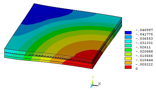
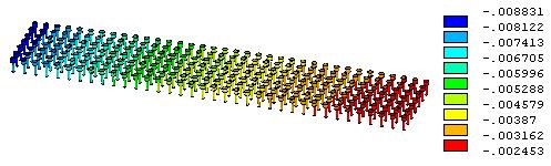
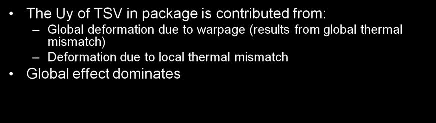
40 40 Global model-displacement U y (@-40 C) 7X36 Global warpage dominates Uy TSV array Die #2 Die #1 Uy
 von Mises")


41 41 Global-Sub model C) von Mises Global model von Mises Sub model von Mises Inter-Chip bumps are more critical than in the TSV region
 Total strain")


42 42 Strains in stacked dice region C) Total strain Plastic strain Creep strain Solder and Cu pillar near the solder interface experience high strains, especially near the solder/cu interfaces

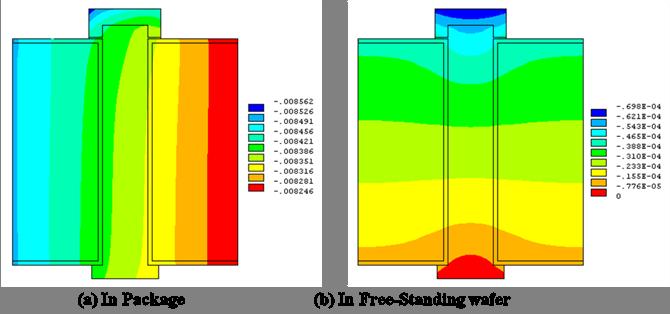
43 TSV in a Package vs. in a Free-Standing C) 43

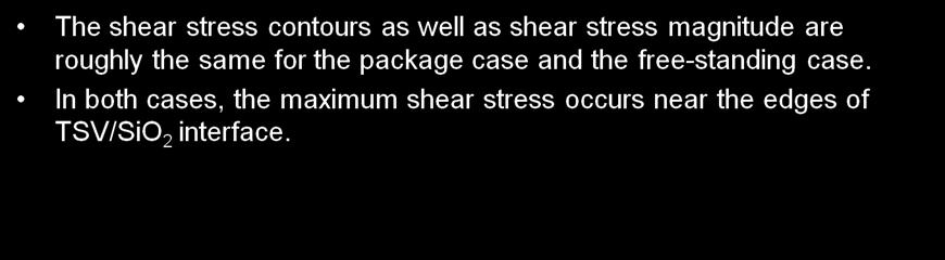
44 TSV in a Package vs. in a Free-Standing Wafer(Interfacial C) 44

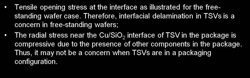
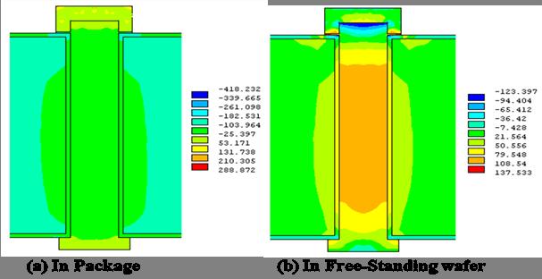
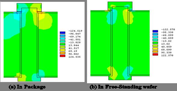
45 TSV in a Package vs. in a Free-Standing Wafer(Radial C) 45
 Higher strains occur in Cu pillar that are bonded to solder material in the packaging configuration compared to the")
46 TSV in a Package vs. in a Free-Standing Wafer(Plastic strain@-40 C) Higher strains occur in Cu pillar that are bonded to solder material in the packaging configuration compared to the unconstrained Cu pillar in a free-standing wafer, and thus the critical location has shifted to the microbump region for a packaging configuration. 46
 TSV/microbump")


47 47 TSV location effect C) TSV/microbump array Equivalent plastic strain of TSVs/microbumps in the packages Creep strain TSVs/bumps near the corners and edges of TSV array have larger stress/strain
48 Summary Cu pumping/sinking is a concern with Cu burden Annular and circular vias are preferable over square vias In the selected design parameter range, the effect of wafer thickness and pitch on the stress/strain is small Voids in Cu help against dielectric cracking; however, Cu cracking will be a concern In 3D package, global thermal/loading effect dominates overall displacement In 3D package, microbumps are more critical than TSVs Experimental validation of the failure mechanisms will be carried out 48
Cu Pillar Interconnect and Chip-Package-Interaction (CPI) for Advanced Cu Low K chip
 for Advanced Cu Low K chip") EPRC 12 Project Proposal Cu Pillar Interconnect and Chip-Package-Interaction (CPI) for Advanced Cu Low K chip 15 th Aug 2012 Page 1 Introduction: Motivation / Challenge Silicon device with ultra low k
EPRC 12 Project Proposal Cu Pillar Interconnect and Chip-Package-Interaction (CPI) for Advanced Cu Low K chip 15 th Aug 2012 Page 1 Introduction: Motivation / Challenge Silicon device with ultra low k
Effects of Design, Structure and Material on Thermal-Mechanical Reliability of Large Array Wafer Level Packages
 Effects of Design, Structure and Material on Thermal-Mechanical Reliability of Large Array Wafer Level Packages Bhavesh Varia 1, Xuejun Fan 1, 2, Qiang Han 2 1 Department of Mechanical Engineering Lamar
Reliability Challenges for 3D Interconnects:
 Reliability Challenges for 3D Interconnects: A material and design perspective Paul S. Ho Suk-Kyu Ryu, Kuan H. (Gary) Lu, Qiu Zhao, Jay Im and Rui Huang The University of Texas at Austin 3D Sematech Workshop,
curamik CERAMIC SUBSTRATES AMB technology Design Rules Version #04 (09/2015)
") curamik CERAMIC SUBSTRATES AMB technology Design Rules Version #04 (09/2015) Content 1. Geometric properties 1.01. Available ceramic types / thicknesses... 03 1.02. thicknesses (standard)... 03 3. Quality
curamik CERAMIC SUBSTRATES AMB technology Design Rules Version #04 (09/2015) Content 1. Geometric properties 1.01. Available ceramic types / thicknesses... 03 1.02. thicknesses (standard)... 03 3. Quality
Experience in Applying Finite Element Analysis for Advanced Probe Card Design and Study. Krzysztof Dabrowiecki Jörg Behr
 Experience in Applying Finite Element Analysis for Advanced Probe Card Design and Study Krzysztof Dabrowiecki Jörg Behr Overview A little bit of history in applying finite element analysis for probe card
3D FRACTURE MECHANICS ANALYSIS OF UNDERFILL DELAMINATION FOR FLIP CHIP PACKAGES
 3D FRACTURE MECHANICS ANALYSIS OF UNDERFILL DELAMINATION FOR FLIP CHIP PACKAGES Zhen Zhang, Charlie J Zhai, and Raj N Master Advanced Micro Devices, Inc. 1050 E. Arques Ave., Sunnyvale, CA 94085, USA Phone:
Micro-tube insertion into aluminum pads: Simulation and experimental validations
 Micro-tube insertion into aluminum pads: Simulation and experimental validations A. Bedoin, B. Goubault, F. Marion, M. Volpert, F. Berger, A. Gueugnot, H. Ribot CEA, LETI, Minatec Campus 17, rue des Martyrs
Thermo-Mechanical FEM Analysis of Lead Free and Lead Containing Solder for Flip Chip Applications
 Thermo-Mechanical FEM Analysis of Lead Free and Lead Containing Solder for Flip Chip Applications M. Gonzalez 1, B. Vandevelde 1, Jan Vanfleteren 2 and D. Manessis 3 1 IMEC, Kapeldreef 75, 3001, Leuven,
Parametric Design and Reliability Analysis of Wire Interconnect Technology Wafer Level Packaging
 Y. T. Lin Graduate Assistant C. T. Peng Graduate Assistant K. N. Chiang Associate Professor e-mail: Knchiang@pme.nthu.edu.tw Dept. of Power Mechanical Engineering, National Tsing Hua University, HsinChu
Micro-Electro-Mechanical Systems (MEMS) Fabrication. Special Process Modules for MEMS. Principle of Sensing and Actuation
 Fabrication. Special Process Modules for MEMS. Principle of Sensing and Actuation") Micro-Electro-Mechanical Systems (MEMS) Fabrication Fabrication Considerations Stress-Strain, Thin-film Stress, Stiction Special Process Modules for MEMS Bonding, Cavity Sealing, Deep RIE, Spatial forming
Micro-Electro-Mechanical Systems (MEMS) Fabrication Fabrication Considerations Stress-Strain, Thin-film Stress, Stiction Special Process Modules for MEMS Bonding, Cavity Sealing, Deep RIE, Spatial forming
Simulation of Embedded Components in PCB Environment and Verification of Board Reliability
 Simulation of Embedded Components in PCB Environment and Verification of Board Reliability J. Stahr, M. Morianz AT&S Leoben, Austria M. Brizoux, A. Grivon, W. Maia Thales Global Services Meudon-la-Forêt,
System Level Effects on Solder Joint Reliability
 System Level Effects on Solder Joint Reliability Maxim Serebreni 2004 2010 Outline Thermo-mechanical Fatigue of solder interconnects Shear and tensile effects on Solder Fatigue Effect of Glass Style on
IMPLEMENTATION OF A FULLY MOLDED FAN-OUT PACKAGING TECHNOLOGY
 IMPLEMENTATION OF A FULLY MOLDED FAN-OUT PACKAGING TECHNOLOGY B. Rogers, C. Scanlan, and T. Olson Deca Technologies, Inc. Tempe, AZ USA boyd.rogers@decatechnologies.com ABSTRACT Fan-Out Wafer-Level Packaging
TSV Interposer Process Flow with IME 300mm Facilities
 TSV Interposer Process Flow with IME 300mm Facilities Property of Institute of Microelectronics (IME)-Singapore August 17, 2012 Outline 1. TSV interposer (TSI) cross sectional schematic TSI with BEOL,
Copyright 2009 Year IEEE. Reprinted from 2009 Electronic Components and Technology Conference. Such permission of the IEEE does not in any way imply
 Copyright 2009 Year IEEE. Reprinted from 2009 Electronic Components and Technology Conference. Such permission of the IEEE does not in any way imply IEEE endorsement of any of Institute of Microelectronics
TSV Processing and Wafer Stacking. Kathy Cook and Maggie Zoberbier, 3D Business Development
 TSV Processing and Wafer Stacking Kathy Cook and Maggie Zoberbier, 3D Business Development Outline Why 3D Integration? TSV Process Variations Lithography Process Results Stacking Technology Wafer Bonding
Evaluation of Cu Pillar Chemistries
 Presented at 2016 IMAPS Device Packaging Evaluation of Cu Pillar Chemistries imaps Device Packaging Conference Spring 2016 Matthew Thorseth, Mark Scalisi, Inho Lee, Sang-Min Park, Yil-Hak Lee, Jonathan
Study of Cracking of Thin Glass Interposers Intended for Microelectronic Packaging Substrates
 Study of Cracking of Thin Glass Interposers Intended for Microelectronic Packaging Substrates Scott R. McCann 1,2, Yoichiro Sato 3, Venkatesh Sundaram 1,4, Rao R. Tummala 1,4,5, and Suresh K. Sitaraman
Jeong et al.: Effect of the Formation of the Intermetallic Compounds (1/7)
") Jeong et al.: Effect of the Formation of the Intermetallic Compounds (1/7) Effect of the Formation of the Intermetallic Compounds between a Tin Bump and an Electroplated Copper Thin Film on both the Mechanical
Jeong et al.: Effect of the Formation of the Intermetallic Compounds (1/7) Effect of the Formation of the Intermetallic Compounds between a Tin Bump and an Electroplated Copper Thin Film on both the Mechanical
Chips Face-up Panelization Approach For Fan-out Packaging
 Chips Face-up Panelization Approach For Fan-out Packaging Oct. 15, 2015 B. Rogers, D. Sanchez, C. Bishop, C. Sandstrom, C. Scanlan, TOlson T. REV A Background on FOWLP Fan-Out Wafer Level Packaging o Chips
Field Condition Reliability Assessment for SnPb and SnAgCu Solder Joints in Power Cycling Including Mini Cycles
 Field Condition Reliability Assessment for SnPb and SnAgCu Solder Joints in Power Cycling Including Mini Cycles Min Pei 1, Xuejun Fan 2 and Pardeep K. Bhatti 2 1 Georgia Tech, 801 Ferst Dr. NW, Atlanta,
Avatrel Stress Buffer Coatings: Low Stress Passivation and Redistribution Applications
 Avatrel Stress Buffer Coatings: Low Stress Passivation and Redistribution Applications Ed Elce, Chris Apanius, Jeff Krotine, Jim Sperk, Andrew Bell, Rob Shick* Sue Bidstrup-Allen, Paul Kohl Takashi Hirano,
NANOINDENTATION OF SILICON CARBIDE WAFER COATINGS
 NANOINDENTATION OF SILICON CARBIDE WAFER COATINGS Prepared by Jesse Angle 6 Morgan, Ste156, Irvine CA 9618 P: 949.461.99 F: 949.461.93 nanovea.com Today's standard for tomorrow's materials. 010 NANOVEA
178 IEEE TRANSACTIONS ON COMPONENTS, PACKAGING AND MANUFACTURING TECHNOLOGY, VOL. 7, NO. 2, FEBRUARY 2017
 178 IEEE TRANSACTIONS ON COMPONENTS, PACKAGING AND MANUFACTURING TECHNOLOGY, VOL. 7, NO. 2, FEBRUARY 2017 Experimental and Theoretical Assessment of Thin Glass Substrate for Low Warpage Scott McCann, Vanessa
Structural Vessel Repairs Using Automated Weld Overlays
 Structural Vessel Repairs Using Automated Weld Overlays Mahmod Samman, Ph.D., P.E. mms@hes.us.com Houston Engineering Solutions, LLC Eric Williams George Gemmel ewilliams@cimsltd.com ggemmell@cimsltd.com
Available online at ScienceDirect. Procedia Engineering 79 (2014 )
") Available online at www.sciencedirect.com ScienceDirect Procedia Engineering 79 (2014 ) 333 338 37th National Conference on Theoretical and Applied Mechanics (37th NCTAM 2013) & The 1st International Conference
Available online at www.sciencedirect.com ScienceDirect Procedia Engineering 79 (2014 ) 333 338 37th National Conference on Theoretical and Applied Mechanics (37th NCTAM 2013) & The 1st International Conference
Novel Materials and Activities for Next Generation Package. Hitachi Chemical., Co.Ltd. Packaging Solution Center Hiroaki Miyajima
 Novel Materials and Activities for Next Generation Package Hitachi Chemical., Co.Ltd. Packaging Solution Center Hiroaki Miyajima 1. Activities of Packaging Solution Center 2. Novel Materials for Next Gen.
Figure 2.3 (cont., p. 60) (e) Block diagram of Pentium 4 processor with 42 million transistors (2000). [Courtesy Intel Corporation.
 (e) Block diagram of Pentium 4 processor with 42 million transistors (2000). [Courtesy Intel Corporation.") Figure 2.1 (p. 58) Basic fabrication steps in the silicon planar process: (a) oxide formation, (b) selective oxide removal, (c) deposition of dopant atoms on wafer, (d) diffusion of dopant atoms into exposed
Figure 2.1 (p. 58) Basic fabrication steps in the silicon planar process: (a) oxide formation, (b) selective oxide removal, (c) deposition of dopant atoms on wafer, (d) diffusion of dopant atoms into exposed
YIELD & TENSILE STRENGTH OF STEEL & ALUMINIUM USING MICROINDENTATION
 YIELD & TENSILE STRENGTH OF STEEL & ALUMINIUM USING MICROINDENTATION Prepared by Duanjie Li, PhD & Pierre Leroux 6 Morgan, Ste156, Irvine CA 9618 P: 949.461.99 F: 949.461.93 nanovea.com Today's standard
Topography and Deformation Measurement and FE Modeling Applied to substrate-mounted large area wafer-level packages (including stacked dice and TSVs)
") Topography and Deformation Measurement and FE Modeling Applied to substrate-mounted large area wafer-level packages (including stacked dice and TSVs) M. Hertl Insidix, 24 rue du Drac, 38180 Grenoble/Seyssins,
Topography and Deformation Measurement and FE Modeling Applied to substrate-mounted large area wafer-level packages (including stacked dice and TSVs) M. Hertl Insidix, 24 rue du Drac, 38180 Grenoble/Seyssins,
3D Package Technologies Review with Gap Analysis for Mobile Application Requirements. Apr 22, 2014 STATS ChipPAC Japan
 3D Package Technologies Review with Gap Analysis for Mobile Application Requirements Apr 22, 2014 STATS ChipPAC Japan T.Nishio Contents Package trends and roadmap update Advanced technology update Fine
Recent Advances in Die Attach Film
 Recent Advances in Die Attach Film Frederick Lo, Maurice Leblon, Richard Amigh, and Kevin Chung. AI Technology, Inc. 70 Washington Road, Princeton Junction, NJ 08550 www.aitechnology.com Abstract: The
UTILIZATION OF ATMOSPHERIC PLASMA SURFACE PREPARATION TO IMPROVE COPPER PLATING PROCESSES.
 SESSION 14 MATERIALS AND PROCESSES FOR ADVANCED PACKAGING UTILIZATION OF ATMOSPHERIC PLASMA SURFACE PREPARATION TO IMPROVE COPPER PLATING PROCESSES. Eric Schulte 1, Gilbert Lecarpentier 2 SETNA Corporation
Reliability Evaluation of CIF (chip-in-flex) and COF (chip-on-flex) packages
 and COF (chip-on-flex) packages") Reliability Evaluation of CIF (chip-in-flex) and COF (chip-on-flex) packages Jae-Won Jang* a, Kyoung-Lim Suk b, Kyung-Wook Paik b, and Soon-Bok Lee a a Dept. of Mechanical Engineering, KAIST, 335 Gwahangno
Reliability Evaluation of CIF (chip-in-flex) and COF (chip-on-flex) packages Jae-Won Jang* a, Kyoung-Lim Suk b, Kyung-Wook Paik b, and Soon-Bok Lee a a Dept. of Mechanical Engineering, KAIST, 335 Gwahangno
Ultra Fine Pitch Bumping Using e-ni/au and Sn Lift-Off Processes
 Ultra Fine Pitch Bumping Using e-ni/au and Sn Lift-Off Processes Andrew Strandjord, Thorsten Teutsch, and Jing Li Pac Tech USA Packaging Technologies, Inc. Santa Clara, CA USA 95050 Thomas Oppert, and
2.5D and 3D Semiconductor Package Technology: Evolution and Innovation
 2.5D and 3D Semiconductor Package Technology: Evolution and Innovation Vern Solberg Solberg Technical Consulting Saratoga, California USA Abstract The electronics industry is experiencing a renaissance
EFFECT OF LOCAL WALL THINNING ON FRACTURE BEHAVIOR OF STRAIGHT PIPE
 ECF EFFECT OF LOCAL WALL THINNING ON FRACTURE BEHAVIOR OF STRAIGHT PIPE Masato Ono, Ki-Woo Nam*, Koji Takahashi, Kotoji Ando Department of Safety & Energy Engineering, Yokohama National University 79-
Low Cycle Fatigue Testing of Ball Grid Array Solder Joints under Mixed-Mode Loading Conditions
 Tae-Sang Park Mechatronics & Manufacturing Technology Center, Corporate Technology Operations, Samsung Electronics Co., LTD, 416, Maetan-3Dong, Yeongtong-Gu, Suwon-City, Gyeonggi-Do, 443-742, Korea e-mail:
Lead-Free Solder Bump Technologies for Flip-Chip Packaging Applications
 Lead-Free Solder Bump Technologies for Flip-Chip Packaging Applications Zaheed S. Karim 1 and Jim Martin 2 1 Advanced Interconnect Technology Ltd. 1901 Sunley Centre, 9 Wing Yin Street, Tsuen Wan, Hong
Manufacturing and Reliability Modelling
 Manufacturing and Reliability Modelling Silicon Chip C Bailey University of Greenwich London, England Printed Circuit Board Airflow Temperature Stress at end of Reflow Stress Product Performance in-service
Introduction to Engineering Materials ENGR2000 Chapter 8: Failure. Dr. Coates
 Introduction to Engineering Materials ENGR2000 Chapter 8: Failure Dr. Coates Canopy fracture related to corrosion of the Al alloy used as a skin material. 8.2 Fundamentals of Fracture Fracture is the separation
Reliability Assessment of Hydrofoil-Shaped Micro-Pin Fins
 Reliability Assessment of Hydrofoil-Shaped Micro-Pin Fins 1 David C. Woodrum, 2 Xuchen Zhang, 1 Peter A. Kottke, 1 Yogendra K. Joshi, 1 Andrei G. Fedorov, 2 Muhannad S. Bakir, and 1 Suresh K. Sitaraman
4th Annual International Conference on Material Science and Engineering (ICMSE 2016)
") Effect of Layer Thickness on Natural Frequency of the Adhesively Bonded Steel Disc Structure Min YOU 1, 2, a,*, Ying-Ying LI 1, b, Jian-Li LI 2, c and Wen-Jun LIU 1, d 1 Hubei Key Laboratory of Hydroelectric
Effect of Layer Thickness on Natural Frequency of the Adhesively Bonded Steel Disc Structure Min YOU 1, 2, a,*, Ying-Ying LI 1, b, Jian-Li LI 2, c and Wen-Jun LIU 1, d 1 Hubei Key Laboratory of Hydroelectric
Power Electronics Packaging Solutions for Device Junction Temperature over 220 o C
 EPRC 12 Project Proposal Power Electronics Packaging Solutions for Device Junction Temperature over 220 o C 15 th August 2012 Page 1 Motivation Increased requirements of high power semiconductor device
A Review of Suitability for PWHT Exemption Requirements in the Aspect of Residual Stresses and Microstructures
 Transactions, SMiRT-23 Division IX, Paper ID 612 (inc. assigned division number from I to X) A Review of Suitability for PWHT Exemption Requirements in the Aspect of Residual Stresses and Microstructures
A STUDY OF FINE BLANKING PROCESS BY FEM SIMULATION. G. Fang, P. Zeng
 Key Engineering Materials Vols. 261-263 (2004) pp 603-608 Online available since 2004/Apr/15 at www.scientific.net (2004) Trans Tech Publications, Switzerland doi:10.4028/www.scientific.net/kem.261-263.603
Board Level Reliability Improvement in ewlb (Embedded Wafer Level BGA) Packages
 Packages") Board Level Reliability Improvement in ewlb (Embedded Wafer Level BGA) Packages by Seng Guan Chow, Yaojian Lin, Bernard Adams * and Seung Wook Yoon** STATS ChipPAC Ltd. 5 Yishun Street 23, Singapore 768442
Board Level Reliability Improvement in ewlb (Embedded Wafer Level BGA) Packages by Seng Guan Chow, Yaojian Lin, Bernard Adams * and Seung Wook Yoon** STATS ChipPAC Ltd. 5 Yishun Street 23, Singapore 768442
Silicon Interposer with Embedded Microfluidic Cooling for High-Performance Computing Systems
 Silicon Interposer with Embedded Microfluidic Cooling for High-Performance Computing Systems Li Zheng 1, Yang Zhang, Xuchen Zhang and Muhannad S. Bakir 2 School of Electrical and Computer Engineering Georgia
SCV Chapter, CPMT Society, IEEE September 14, Voids at Cu / Solder Interface and Their Effects on Solder Joint Reliability
 Voids at / Solder Interface and Their Effects on Solder Joint Reliability Zequn Mei, Mudasir Ahmad, Mason Hu, Gnyaneshwar Ramakrishna Manufacturing Technology Group Cisco Systems, Inc. Acknowledgement:
Introduction to Joining Processes
 4. TEST METHODS Joints are generally designed to support a load, and must be tested to evaluate their load-supporting capabilities. However, it is also important to evaluate, not the joint, but rather
Silicon Interposers with Integrated Passive Devices: Ultra-Miniaturized Solution using 2.5D Packaging Platform
 Minapad 2014, May 21 22th, Grenoble; France Silicon Interposers with Integrated Passive Devices: Ultra-Miniaturized Solution using 2.5D Packaging Platform Stéphane Bellenger, Laëtitia Omnès, Jean-René
White Paper Quality and Reliability Challenges for Package on Package. By Craig Hillman and Randy Kong
 White Paper Quality and Reliability Challenges for Package on Package By Craig Hillman and Randy Kong Background Semiconductor technology advances have been fulfilling Moore s law for many decades. However,
Design for Flip-Chip and Chip-Size Package Technology
 Design for Flip-Chip and Chip-Size Package Technology Vern Solberg Solberg Technology Consulting Madison, Wisconsin Abstract As new generations of electronic products emerge they often surpass the capability
Achieving Warpage-Free Packaging: A Capped-Die Flip Chip Package Design
 Achieving Warpage-Free Packaging: A Capped-Die Flip Chip Package Design Yuci Shen *1, Leilei Zhang ** and Xuejun Fan * * Lamar University, Beaumont, Texas ** NVIDIA Corporation, Santa Clara, California
Residual Stress Analysis in Injection Moulded Polycarbonate Samples
 Residual Stress Analysis in Injection Moulded Polycarbonate Samples Arnaud Magnier 1a*, Berthold Scholtes 1b, Thomas Niendorf 1c 1 Institute of Materials Engineering, University of Kassel, Germany a magnier@uni-kassel.de,
3D-WLCSP Package Technology: Processing and Reliability Characterization
 3D-WLCSP Package Technology: Processing and Reliability Characterization, Paul N. Houston, Brian Lewis, Fei Xie, Ph.D., Zhaozhi Li, Ph.D.* ENGENT Inc. * Auburn University ENGENT, Inc. 2012 1 Outline Packaging
3D technologies for More Efficient Product Development
 3D technologies for More Efficient Product Development H. Ribot, D. Bloch, S. Cheramy, Y. Lamy, P. Leduc, T. Signamarcheix, G. Simon Semicon Europa, TechArena II, 09 October 2013 Photonics in Product development:
PCB Production Process HOW TO PRODUCE A PRINTED CIRCUIT BOARD
 NCAB Group Seminars PCB Production Process HOW TO PRODUCE A PRINTED CIRCUIT BOARD NCAB GROUP PCB Production Process Introduction to Multilayer PCBs 2 Introduction to multilayer PCB s What is a multilayer
EIPC Summer Conference Luxembourg Paper 4
 EIPC Summer Conference Luxembourg 2013 PCB differentiation through technology - made in Europe Paper 4 Copper plating process for filling micro vias and through via holes with minimum surface deposition
Materials Characterization for Stress Management
 Materials Characterization for Stress Management Ehrenfried Zschech, Fraunhofer IZFP Dresden, Germany Workshop on Stress Management for 3D ICs using TSVs San Francisco/CA, July 13, 2010 Outline Stress
Intel Pentium Processor W/MMX
 Construction Analysis Intel Pentium Processor W/MMX Report Number: SCA 9706-540 Global Semiconductor Industry the Serving Since 1964 15022 N. 75th Street Scottsdale, AZ 85260-2476 Phone: 602-998-9780 Fax:
Nonlinear Finite Element Modeling & Simulation
 Full-Scale Structural and Nonstructural Building System Performance during Earthquakes & Post-Earthquake Fire A Joint Venture between Academe, Industry and Government Nonlinear Finite Element Modeling
Visit
 Practical Applications for Nano- Electronics by Vimal Gopee E-mail: Vimal.gopee@npl.co.uk 10/10/12 Your Delegate Webinar Control Panel Open and close your panel Full screen view Raise hand for Q&A at the
EDGE CHIPPING RESISTANCE USING MACROINDENTATION TESTING
 EDGE CHIPPING RESISTANCE USING MACROINDENTATION TESTING Prepared by Ali Mansouri 6 Morgan, Ste156, Irvine CA 92618 P: 949.461.9292 F: 949.461.9232 nanovea.com Today's standard for tomorrow's materials.
Electrical, Optical and Fluidic Through-Silicon Vias for Silicon Interposer Applications
 Electrical, Optical and Fluidic Through-Silicon Vias for Silicon Interposer Applications Mahavir S. Parekh, Paragkumar A. Thadesar and Muhannad S. Bakir Georgia Institute of Technology, 791 Atlantic Drive,
Carbon-fiber Reinforced Concrete with Short Aramid-fiber Interfacial Toughening
 2016 International Conference on Electronic Information Technology and Intellectualization (ICEITI 2016) ISBN: 978-1-60595-364-9 Carbon-fiber Reinforced Concrete with Short Aramid-fiber Interfacial Toughening
TSV CHIP STACKING MEETS PRODUCTIVITY
 TSV CHIP STACKING MEETS PRODUCTIVITY EUROPEAN 3D TSV SUMMIT 22-23.1.2013 GRENOBLE HANNES KOSTNER DIRECTOR R&D BESI AUSTRIA OVERVIEW Flip Chip Packaging Evolution The Simple World of C4 New Flip Chip Demands
200mm Next Generation MEMS Technology update. Florent Ducrot
 200mm Next Generation MEMS Technology update Florent Ducrot The Most Exciting Industries on Earth Semiconductor Display Solar 20,000,000x reduction in COST PER TRANSISTOR in 30 years 1 20x reduction in
Available online at ScienceDirect. Procedia Engineering 79 (2014 )
") Available online at www.sciencedirect.com ScienceDirect Procedia Engineering 79 (2014 ) 212 217 37th National Conference on Theoretical and Applied Mechanics (37th NCTAM 2013) & The 1st International Conference
Available online at www.sciencedirect.com ScienceDirect Procedia Engineering 79 (2014 ) 212 217 37th National Conference on Theoretical and Applied Mechanics (37th NCTAM 2013) & The 1st International Conference
Effect of Encapsulation Materials on Tensile Stress during Thermo-Mechanical Cycling of Pb-Free Solder Joints
 Effect of Encapsulation Materials on Tensile Stress during Thermo-Mechanical Cycling of Pb-Free Solder Joints Maxim Serebreni, Dr. Nathan Blattau, Dr. Gilad Sharon, Dr. Craig Hillman DfR Solutions Beltsville,
28nm Mobile SoC Copper Pillar Probing Study. Jose Horas (Intel Mobile Communications) Amy Leong (MicroProbe) Darko Hulic (Nikad)
 Amy Leong (MicroProbe) Darko Hulic (Nikad)") 28nm Mobile SoC Copper Pillar Probing Study Jose Horas (Intel Mobile Communications) Amy Leong (MicroProbe) Darko Hulic (Nikad) Overview Introduction to IMC Copper Pillar Implementation at IMC Low force
28nm Mobile SoC Copper Pillar Probing Study Jose Horas (Intel Mobile Communications) Amy Leong (MicroProbe) Darko Hulic (Nikad) Overview Introduction to IMC Copper Pillar Implementation at IMC Low force
Thermal Symposium August Minteq International, Inc. Pyrogenics Group A Thermal Management Solution for State-of-the-Art Electronics
 Thermal Symposium August 9-10 2017 Minteq International, Inc. Pyrogenics Group A Thermal Management Solution for State-of-the-Art Electronics Mark Breloff Technical Sales Manager 1 Electronics power requirements
Modelling Embedded Die Systems
 Modelling Embedded Die Systems Stoyan Stoyanov and Chris Bailey Computational Mechanics and Reliability Group (CMRG) University of Greenwich, London, UK 22 September 2016 IMAPS/NMI Conference on EDT Content
2015 IEEE. REPRINTED, WITH PERMISSION, FROM Next Generation Metallization Technique for IC Package Application
 2015 IEEE. REPRINTED, WITH PERMISSION, FROM Next Generation Metallization Technique for IC Package pplication Yoshiyuki Hakiri, Katsuhiro Yoshida, Shenghua Li, Makoto Kondoh, Shinjiro Hayashi The Dow Chemical
Determination of Failure Strength of Flat Plate Weld Joint Using Finite Element Analysis
 International Journal of Scientific & Engineering Research Volume 3, Issue 12, December-2012 1 Determination of Failure Strength of Flat Plate Weld Joint Using Finite Element Analysis M. V. Dalvi 1, Mrs.
A Solder Joint Reliability Model for the Philips Lumileds LUXEON Rebel LED Carrier Using Physics of Failure Methodology
 A Solder Joint Reliability Model for the Philips Lumileds LUXEON Rebel LED Carrier Using Physics of Failure Methodology Rudi Hechfellner 1, Michiel Kruger 1, Tewe Heemstra 2 Greg Caswell 3, Nathan Blattau
FABRICATION AND RELIABILITY OF ULTRA-FINE RDL STRUCTURES IN ADVANCED PACKAGING BY EXCIMER LASER ABLATION
 FABRICATION AND RELIABILITY OF ULTRA-FINE RDL STRUCTURES IN ADVANCED PACKAGING BY EXCIMER LASER ABLATION NCCAVS Joint Users Group Technical Symposium San Jose, June 7 th, 2017 Markus Arendt, SÜSS MicroTec
Board-Level Reliability of 3D Through Glass Via Filters During Thermal Cycling
 Board-Level Reliability of 3D Through Glass Via Filters During Thermal Cycling Scott McCann 12*, Satoru Kuramochi 3, Hobie Yun 4, Venkatesh Sundaram 1, M. Raj Pulugurtha 1, Rao R. Tummala 1, and Suresh
Endurance testing and FE analysis of four wheeler automobile stabilizer bar
 Endurance testing and FE analysis of four wheeler automobile stabilizer bar P.Senapathi, S.Shamasundar, G. Venugopala Rao and B.M.Sachin ProSIM R&D Center,Bangalore. Krishna Srinivas, N.Dasari, Cheryl
Rockwell R RF to IF Down Converter
 Construction Analysis Rockwell R6732-13 RF to IF Down Converter Report Number: SCA 9709-552 Global Semiconductor Industry the Serving Since 1964 17350 N. Hartford Drive Scottsdale, AZ 85255 Phone: 602-515-9780
Study on Mixed Mode Crack-tip Plastic Zones in CTS Specimen
 Proceedings of the World Congress on Engineering Vol II WCE, July -,, London, U.K. Study on Mixed Mode Crack-tip Plastic Zones in Specimen C. M. Sharanaprabhu, S. K. Kudari Member, IAENG Abstract The studies
Wire-bonds Durability in High-temperature Applications M. Klíma, B. Psota, I. Szendiuch
 Ročník 2013 Číslo V Wire-bonds Durability in High-temperature Applications M. Klíma, B. Psota, I. Szendiuch Department of Microelectronics, Faculty of Electrical Engineering and Communication, Brno University
Semiconductor IC Packaging Technology Challenges: The Next Five Years
 SPAY025 May 2006 White Paper Mario A. Bolanos, Director Semiconductor Group Packaging Technology Development, Texas Instruments In the era of communications and entertainment, growth of consumer electronics
TSV-Based Quartz Crystal Resonator Using 3D Integration and Si Packaging Technologies
 TSV-Based Quartz Crystal Resonator Using 3D Integration and Si Packaging Technologies Jian-Yu Shih 1,Yen-Chi Chen 2, Cheng-Hao Chiang 1, Chih-Hung Chiu 2, Yu- Chen Hu 1, Chung-Lun Lo 2, Chi-Chung Chang
An Innovative High Throughput Thermal Compression Bonding Process
 An Innovative High Throughput Thermal Compression Bonding Process Li Ming 2 September 2015 Outline Introduction Throughput improved TCB Process Liquid Phase Contact (LPC) bonding Flux-LPC-TCB under inert
Reliability of Interconnects in LED Lighting Assemblies Utilizing Metal Clad Printed Circuit Boards Stefano Sciolè BDM I.M.S.
 Reliability of Interconnects in LED Lighting Assemblies Utilizing Metal Clad Printed Circuit Boards Stefano Sciolè BDM I.M.S. Henkel Electronic Materials Agenda 1. Introduction 2. Motivation 3. Interconnect
KGC SCIENTIFIC Making of a Chip
 KGC SCIENTIFIC www.kgcscientific.com Making of a Chip FROM THE SAND TO THE PACKAGE, A DIAGRAM TO UNDERSTAND HOW CPU IS MADE? Sand CPU CHAIN ANALYSIS OF SEMICONDUCTOR Material for manufacturing process
BENDING STRENGTH OF SOLDER JOINTS AS A FUNCTION OF JOINT LENGTH
 As originally published in the SMTA Proceedings. BENDING STRENGTH OF SOLDER JOINTS AS A FUNCTION OF JOINT LENGTH Saeed Akbari, Amir Nourani, Jan K. Spelt University of Toronto Toronto, ON, Canada spelt@mie.utoronto.ca
Types of Strain. Engineering Strain: e = l l o. Shear Strain: γ = a b
 Types of Strain l a g Engineering Strain: l o l o l b e = l l o l o (a) (b) (c) Shear Strain: FIGURE 2.1 Types of strain. (a) Tensile. (b) Compressive. (c) Shear. All deformation processes in manufacturing
Flip-Chip Process Improvements for Low Warpage
 Flip-Chip Process Improvements for Low Warpage Robert L. Hubbard Lambda Technologies, Inc. Morrisville, NC, USA bhubbard@microcure.com Pierino Zappella*, Pukun Zhu Henkel Corporation Irvine, CA, USA Abstract
Fatigue of metals. Subjects of interest
 Fatigue of metals Chapter 12 Subjects of interest Objectives / Introduction Stress cycles The S-N curve Cyclic stress-strain curve Low cycle fatigue Structural features of fatigue Fatigue crack propagation
M3 Review Automated Nanoindentation
 M3 Review Automated Nanoindentation Prepared by Duanjie Li, PhD & Pierre Leroux 6 Morgan, Ste156, Irvine CA 92618 P: 949.461.9292 F: 949.461.9232 nanovea.com Today's standard for tomorrow's materials.
Applications of High-Performance MEMS Pressure Sensors Based on Dissolved Wafer Process
 Applications of High-Performance MEMS Pressure Sensors Based on Dissolved Wafer Process Srinivas Tadigadapa and Sonbol Massoud-Ansari Integrated Sensing Systems (ISSYS) Inc., 387 Airport Industrial Drive,
FATIGUE ANALYSIS OF A NOTCHED CANTILEVER BEAM USING ANSYS WORKBENCH. N. Sinan Köksal, Arif Kayapunar and Mehmet Çevik
 Proceedings of the Fourth International Conference on Mathematical and Computational Applications June 11-13, 2013. Manisa, Turkey, pp.111-118 FATIGUE ANALYSIS OF A NOTCHED CANTILEVER BEAM USING ANSYS
EE C245 ME C218 Introduction to MEMS Design Fall 2011
 Lecture Outline EE C245 ME C218 Introduction to MEMS Design Fall 2011 Prof. Clark T.-C. Nguyen Dept. of Electrical Engineering & Computer Sciences University of California at Berkeley Berkeley, CA 94720
Material Selection and Parameter Optimization for Reliable TMV Pop Assembly
 Selection and Parameter Optimization for Reliable TMV Pop Assembly Brian Roggeman, David Vicari Universal Instruments Corp. Binghamton, NY, USA Roggeman@uic.com Martin Anselm, Ph.D. - S09_02.doc Lee Smith,
Effect of Sheet Thickness and Type of Alloys on the Springback Phenomenon for Cylindrical Die
 AMERICAN JOURNAL OF SCIENTIFIC AND INDUSTRIAL RESEARCH 01, Science Huβ, http://www.scihub.org/ajsir ISSN: 153-69X, doi:10.551/ajsir.01.3.6.80.86 Effect of Sheet Thickness and Type of Alloys on the Springback
Investigation of Interface Delamination of EMC-Copper Interfaces in Molded Electronic packages
 Agenda Investigation of Interface Delamination of EMC-Copper Interfaces in Molded Electronic packages A.Yadur 1,2, P. Gromala 2, Dipl.-Ing. Axel Mueller 3 1Robert Bosch Engineering and Business Solutions
CHAPTER 11: PRESTRESSED CONCRETE
 CHAPTER 11: PRESTRESSED CONCRETE 11.1 GENERAL (1) This chapter gives general guidelines required for the design of prestressed concrete structures or members with CFRM tendons or CFRM tendons in conjunction
1E5 Advanced design of glass structures. Martina Eliášová
 1E5 Advanced design of glass structures Martina Eliášová List of lessons 1) History, chemical, production 2) Glass as a material for load bearing structures 3) Design of laminated plates 4) Design of glass