Recent Developments in the Field of Silicon Solar Cell Technology
|
|
|
- Hillary Houston
- 5 years ago
- Views:
Transcription

1 Recent Developments in the Field of Silicon Solar Cell Technology Daniel Biro Fraunhofer Institute for Solar Energy Systems ISE World of Energy Solutions Stuttgart 30. September 2013

2 Agenda Market Development General Crystalline Silicon Solar Cell Aspects Recent Advancements Summary

3 Market Development three years ago Overall PV market 2009: 7 GWp 2010: 15 GWp estimated German feed in tariff stimulated a large market share Strong ramp up of PV-Production capacity especially in Asia German PV-equipment boom Last but not least: silicon shortage

4 Market Development Recent Installation Cost /kwp System price Roof-mounted

5 Market Development PV has become a commodity solarserver.de Heindl Server GmbH

6 Market Development 2012 Installations +30 GW Overall PV market Already 2011 and 2012 were 30 GW Surprise : Overcapacity Source: EPIA Global Market Outlook for Photovoltaics
7 Market Development Future Market Sarasin Bank, Nov 2010: 110 Gigawatt 2020 Marktausblick: 30 GW/a für 2014, 110 GW/a für 2020 Jährl. Wachstumsrate: Im Bereich 20% bis 30% Mit 30 GW 2012 bereits weit über 2010 Vorhersage! Quelle: Sarasin, Solar Strudy, Nov 2010

8 Market Development PV Equipment Book-to-Bill Ratio Source: July 3, 2013 SEMI reported the worldwide PV manufacturing equipment billings and bookings for the first quarter of 2013 Book-to-Bill Ratio drops below parity by Q2/2011 Slowly recovering in 2013 but sill below parity

9 Which type of material? Cumulative PV Production: 89% c-silicon p-type multi 56% p-type mono 28% n-type 5% Si seems to be a very good choice Which is the further potential of Si?

10 Standard Solar Cells today Front Surface Layout: Cell Size 156x156 mm² Three busbars allow interconnection Current Efficiencies: Multicrystalline ~17,5% Monocrystalline ~19 % Power single cell up to: ~ 4,7 Watts Source :

11 Standard Silicon Solar Cells Today Rear Surface Cell Rear surface Al-BSF: Passivation quality: S back ~500 cm/s Internal reflection: R ~ % Challenging for very thin wafers Source :
 Contact firing p-type")
12 State-Of-The-Art Industrial Solar Cell Process Saw damage removal / Texture and cleaning Deposition of dopant source Diffusion Removal of PSG and rear emitter Deposition of SiN x ARC Screen printing of contacts (Al, AgAl, Ag) Contact firing p-type Si-wafer
13 State-Of-The-Art Industrial Solar Cell Process Saw damage removal / Texture and cleaning Deposition of dopant source Diffusion Phosphorus Silicate- Glass (PSG) Removal of PSG and rear emitter Deposition of SiN x ARC Screen printing of contacts (Al, AgAl, Ag) Contact firing n-type emitter p-type Si-wafer
14 State-Of-The-Art Industrial Solar Cell Process Saw damage removal / Texture and cleaning Deposition of dopant source Diffusion Removal of PSG and rear emitter Deposition of SiN x ARC Screen printing of contacts (Al, AgAl, Ag) Contact firing n-type emitter p-type Si-wafer
 Contact firing n-type emitter p-type")
15 State-Of-The-Art Industrial Solar Cell Process Saw damage removal / Texture and cleaning Deposition of dopant source Diffusion SiN x ARC Removal of PSG and rear emitter Deposition of SiNx ARC Screen printing of contacts (Al, AgAl, Ag) Contact firing n-type emitter p-type Si-wafer
16 State-Of-The-Art Industrial Solar Cell Process Saw damage removal / Texture and cleaning Front contacts (Ag) Deposition of dopant source Diffusion SiN x ARC Removal of PSG and rear emitter Deposition of SiN x ARC Screen printing of contacts (Al, AgAl, Ag) n-type emitter Contact firing Contact pads (AgAl) Rear contact (Al) p-type Si-wafer
17 State-Of-The-Art Industrial Solar Cell Process Saw damage removal / Texture and cleaning Front contacts (Ag) Deposition of dopant source Diffusion SiN x ARC Removal of PSG and rear emitter Deposition of SiN x ARC Screen printing of contacts (Al, AgAl, Ag) Contact firing Al BSF Contact pads (AgAl) Rear contact (Al) n-type emitter p-typ Si-wafer
18 What to do? Let s see how we can improve the silicon cell : Evolution of the standard fabrication process drop-in replacements and small step incremental improvements advanced cell structures with low impact on module technology Introduction of disruptive improvements major process or structure changes / new technologies possible strong impact on module technology Will stimulate: Interest in new equipment, better materials and processes
19 Incremental improvements Front contact Printed bulk contact Plating: Seed and growth The Million Dollar Question Selective emitter

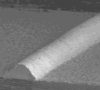
 Flexographic printing, width <30µm height ~20µm Breite")
20 Potential for Improvement? Advanced Metallization One-step approach: advanced screen/stencil printing, Dispensing width µm height µm Two-step approach: seed + plate different seed layer technologies: Screen printing Screen printed contact (one-step) Flexographic printing, width <30µm height ~20µm Breite <60µm Höhe >30µm Seed layer with low Ag lay down Dispensed contact (one-step) 20

 Potential for high")

21 Advanced Front Metallization Seed layer: Flexographic printing Printing of fine-line seedlayer fingers First solar cells (156 x 156 cm²) realised with flexographic printing (seed layer width ~25µm) Potential for high troughput (roll-to-wafer) Significant Ag-reduction possible with subsequent Ni/Cu/Ag plating Printing principle 21


22 Advanced Front Metallization Seed layer: Flexographic printing Fine-line seedlayer metallization with flexographic printing (results): Cz-Si, printed Ag-Seedlayer 22 M. Frey et al., 1st Si PV 2010 Freiburg

 Efficiency improval:")


23 Advanced Front Metallization One-step approach: Dispensing v p Finger width significantly reduced Excellent aspect ratio (close to 1) Particularly attractive for MWT (no busbar) Efficiency improval: up to 0,5%abs industrial realization (multi-nozzle) ongoing conventional width <30µm height ~20µm 10 nozzle printing process SEM images of a dispensed finger on textured Si 23 M. Pospischil et al., 1st Si PV 2010 Freiburg
24 Incremental improvements Back surface Current Rear Surface Al-BSF Passivation ~500 cm/s Reflectivity 65-75% Printed solder pads Target Rear Surface Passivation ~100 cm/s Reflectivity 95% Local Contacts Solderable surface needed Current rear surface limits efficiency
25 Been here before are we making fossil structures?? PERC (1989): Thermal Oxide passivates rear surface Local point contacts Selective Emitter PERL (1990): Local diffusion added Reduced contact resistance and recombination Since then : Technology development -> replace Photolithography and Complex Contact formation Massive reduction of processing steps -> transfer to industrial lines Transfer to large wafers and reliability testing in modules Source: Blakers et al. APL 55(13), 1989, p
26 Local contact formation on back surface: three options LCO: Local Contact Opening Open the dielectric Metallization subsequently LFC: Laser Fired contacts Metallized first LFC punches Metal through the dielectric Can also be used with PVD Metallization Silicon LCO LFC FTC FTC: Fire Through contact Print two different pastes All fired in 1 Step No additional technology
 Contact firing Process options for passivated rear Saw damage removal / Text.")
27 Passivated Rear surface Current Al-BSF Standard process Saw damage removal / Texture and cleaning Deposition of dopant + Diffusion Removal of PSG and rear emitter Deposition of SiN x ARC Screen printing contacts (Al, AgAl, Ag) Contact firing Process options for passivated rear Saw damage removal / Text., cleaning + polish Deposition of dopant + Diffusion Removal of PSG and rear emitter + (polish) Deposition of SiN x ARC Front and passivation of Rear surface Local rear contacts Further Upgrades possible: Selective emitter Advanced front contacts


28 Incremental improvements Back surface Status passivated rear Passivated rear surface structure proposed in early 1990s R&D has achieved very high efficiencies Industry and industry-oriented research groups developed lean process sequences and transferred these in pilot lines Equipment vendors developed suitable equipment Reliability questions still demanding for many Solar World and Hanwha Q-Cells is already selling certified modules with PERL Cells Maybe less incremental than expected?? large efforts and long time to find non-disruptive sequence!
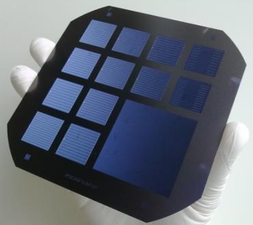
29 Quasi Incremental improvements MWT Cell MWT: Metal Wrap Through The most simple back contact cell Reduce optical loss by shifting the busbars to the rear Pick and place allows thinner wafers in module Boost module performance by more design freedom of interconnects combine good front with improvement on module level
30 Quasi Incremental improvements MWT Cell MWT: Metal Wrap Through The most simple back contact cell Reduce optical loss by shifting the busbars to the rear Pick and place allows thinner wafers in module Boost module performance by more design freedom of interconnects via on cell level % abs. gain possible Cells : Fraunhofer ISE
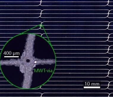
31 Quasi Incremental improvements MWT Cell Rear surface busbars or local pads Rear contact isolation between n- and p-contact via Solder pad location depends on module design Efficiency gain on module level additionally % Total possible gain in module: Up to ~1% absolute Cells : Fraunhofer ISE

32 The MWT-PERC Approach Motivation H-Pattern BSF H-Pattern PERC High rear surface recombination rate High shading losses Poor internal reflectance MWT-BSF Improves light trapping and passivation Advantageous for thin cells Blakers et al., Appl. Phys. Lett. 55, pp , 1989 MWT-PERC Reduces shading losses Allows for novel module concepts Advantages of both structures combined v. Kerschaver et al., Proc. 2nd WCPEC, 1998, pp Dross et al., Proc. 4th WCPEC, 2006, pp
: 18,4% The module was processed")
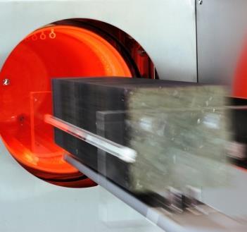
33 HIP-MWT: 60 Cell Module Module Results Lean cell process: 1 extra step hole drilling Cell Efficiencies up to 19.8% IV ISE CalLab PV Modules Module output power: 277 W Efficiency (aperture area): 18,4% The module was processed in a joint project

34 Disruptive Changes of the cell structure and fabrication Example n-type Back Contact Cell n-type substrates Higher Efficiencies possible close to 25% achieved Various promising approaches bifacial approaches interesting Challenges Si-Crystal Growth proprietary technology Third parties try to simplify structure with alternative ideas Will scale effects kick in? Maxeon Third Generation Cell efficiency: ~24% Standard size modules with Power up to: 345 W

35 Disruptive Changes of the cell structure and fabrication Example n-type Hetero Junction Cell n-type substrates Higher Efficiencies possible close to 25% achieved Various promising approaches bifacial approaches interesting Challenges Si-Crystal Growth proprietary technology Third parties try to simplify structure with alternative ideas Will scale effects kick in? R&D Result by Panasonic: 24.7 % Efficiency on cm² (published Feb. 2013)
36 Summary Within last three years PV has completed its transition into a real industry In spite of temporary overcapacity overall strong growth of PV is expected New technologies must be able to improve or beat the standard cell process Even incremental changes are tough to introduce keep it simple! Many improvement options are being evaluated and we see pilot production of PERC and MWT cells after a extensive pipeline process n-type silicon very promising and in production many companies try to catch up with current leaders Avoid interrupted value chain in Europe Continued efforts in R&D to develop advanced technologies

37 Thank You Very Much for Your Attention! Fraunhofer Institute for Solar Energy Systems ISE Daniel Biro 37