Optimization of a Chlorine-Based Deep Vertical Etch of GaN Demonstrating Low Damage and Low Roughness
|
|
|
- Ashley Tate
- 5 years ago
- Views:
Transcription
1 Optimization of a Chlorine-Based Deep Vertical Etch of GaN Demonstrating Low Damage and Low Roughness Running title: Low Damage Cl2/Ar Deep Vertical GaN Etch Running Authors: Tahhan et al. Maher Tahhan a, Joseph Nedy, Silvia H. Chan, Cory Lund, Haoran Li, Geetak Gupta, Stacia Keller, Umesh Mishra Electrical and Computer Engineering Department, UC Santa Barbara, Santa Barbara, California, USA a Electronic mail: maher@ece.ucsb.edu The dry etching of GaN to form deep vertical structures is a critical step in many power device processes. To accomplish this, a chlorine and argon etch is investigated in detail to satisfy several criteria simultaneously such as surface roughness, crystal damage, and etch angle. Etch depths from 2 μm to 3.4 μm are shown in this paper. The authors investigate the formation of etch pits and its contributing factors. In addition, a nickel hard mask process is presented, with an investigation into the causes of micro-masking and a pre-etch to prevent it. The authors show the results of optimized etch conditions resulting in a 2 μm deep, nm rms roughness etch, with a 7.6 o angle from vertical and low surface damage as measured by photoluminescence. I. INTRODUCTION 1
2 GaN is widely used in optoelectronic devices, such as in LEDs and laser diodes, but it also has several applications for electronics, including RF and high power devices. Recent work on GaN based high power switching devices have introduced transistor designs that rely on vertical current conduction. 1,2,3 Such devices tend to require deep etching into GaN for device isolation, current aperture definition, and/or vertical channel formation. 4,5 In some cases the etched surface is part of the active region. This necessitates that the etch be highly controlled and produce little surface damage. Previously, etching of GaN has been attempted via several methods. Vertical c- plane GaN wet etches have shown little promise due to the lack of an isotropic etchant. 6 Focus recently has been on inductively coupled plasma, ICP, etching as it results in more vertical profiles than reactive ion etching, RIE. 7,8 Some have evaluated the damage caused from etching through photoluminescence, cathodoluminescence, and roughness measurements. 9,10,11,12 Etch surface damage has been observed to cause decreases in photoluminescence due to ion damage 10, as well as forming pits and pillars. 12 Hahn et al. 13 reported on the effect of etch mask on etch angle for their BCl 3 /Cl 2 /N 2 etch. A Cl 2 /Ar etch chemistry has been studied as a means to achieve low damage, although only for depths up to 550 nm. 14 In this paper, a chlorine and argon ICP etch is investigated by varying the parameters of the plasma and examining the effects on the surface and the sidewall morphology. The Cl 2 /Ar etch parameters are optimized for surface roughness and low damage, while maintaining a near-vertical sidewall. Surface roughness, etch rate, and etch pit characterization are used to analyze the physical effects of the etch. 2
3 Photoluminescence is used to quantitatively assess damage to the crystal. Sidewall angle is noted for the different masking materials used. II. EXPERIMENT Samples consisted of epitaxially grown 4-6 μm Ga-face GaN on 2 inch sapphire (0001) wafers by metal organic chemical vapor deposition, MOCVD. The roughness of the unetched GaN was approximately 0.23 nm rms. The wafers were each cleaved into six pieces before processing. Before processing, all samples were cleaned in an ultrasonic bath in acetone and isopropanol for 3 minutes each, and rinsed in de-ionized water. Either a photoresist or hard mask was defined on the samples. For samples with a photoresist mask, they underwent a dehydration bake before coating, exposing, and developing the resist. The resist used was SPR coated to a thickness of 7.9 μm and patterned with an i-line stepper. For samples with a hard mask, 50 nm of SiO 2 was first deposited via plasma enhanced chemical vapor deposition, PECVD, to provide a barrier layer to prevent metal contamination. Then the samples were cleaned again and patterned with nlof 2020 before 10 nm of titanium and 180 nm of nickel were deposited via an electron beam evaporation and lift off procedure. Titanium was used as an adhesive layer to the oxide. Nickel was chosen for its low etch rate in Cl 2 /Ar in comparison to GaN. 15 These samples were then etched using CHF3 to remove the exposed SiO2 before the deep GaN etch. All etching was performed using a Panasonic E626I ICP etching system. This system allows for the changing of both the RF bias power and the ICP source power. The gas flows and the chamber pressure can also be modified. Throughout the experiment, the 3
4 ratio between the RF and ICP powers was kept at 1:4. In addition to varying the powers, the total gas flow, the ratio of the gasses, and the chamber pressure during etching was also varied for the experiment. The samples were mounted on a 6 inch silicon wafer before loading into the etching system. Analysis of the samples included atomic force microscopy (AFM) to measure the roughness of the etched lateral surface. This also provided information on pit size and density. Roughness values are reported for scans of 10 x 10 μm 2 areas unless otherwise specified. Scanning electron microscopy (SEM) was used to measure etch depth and sidewall angles, as well to observe sidewall roughness and large pillar and pit formation. A Dektak profilometer and a confocal microscope were used to confirm the etch depth in addition to AFM and SEM. Photoluminescence (PL) was used to detect changes in the crystal quality near the surface by measuring samples before and after etching. For each variable experiment series, pieces from the same two inch wafer were used and measurements were made in the center of each piece. This was done in order to insure that variations in growth between samples did not affect conclusions made about the effects of parameters on the resulting etch. III. RESULTS AND DISCUSSION A. Bias and Source Power Variation For When varying the bias and source powers, the etch time for each was set such that the etch depth reached approximately 2 μm. This is done to reasonably compare results of etches with different rates. As seen in Figure 1, as the power increases, the etch rate increases linearly for the range tested. In addition, the surface roughness decreases with increasing power for equivalent etch depths. These results are in contrast with 4
5 results from Hahn et al. 11 which may have compared different powers for equal time. They show that increasing the source power alone increases the roughness, whereas changing the bias power alone did not affect roughness. Instead the experiment shows that increasing both the source and bias powers simultaneously resulted in lower surface roughness. Figure 2 shows the features that contribute the most to the surface roughness. Morphology change from ridges to pits can be seen for samples etched at 200 W and 400 W ICP power, respectively. For the lowest power of 100 W, relatively large hills form with peaks on the order of 40 nm. For all further experiments, an ICP source power of 300 W and RF bias power of 75 W is used. This power, in between the highest two powers in this series, does not form ridges or hills, and has smaller pits. For this series, flow rates of 20 sccm each of chlorine and argon were used at 1 Pa. 5

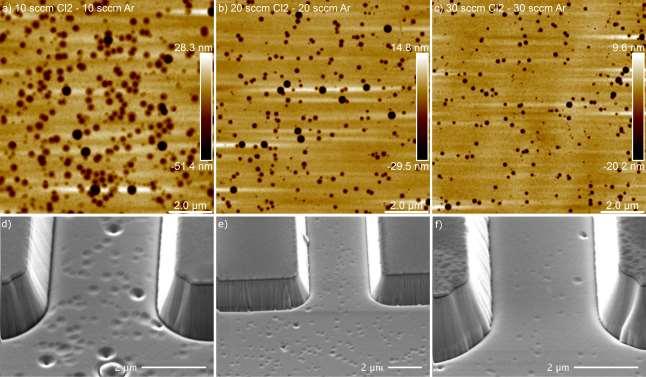
6 B. Gas Flow and Pressure Variation The total gas flow rate was changed from 20 sccm to 60 sccm while keeping the Cl 2 /Ar ratio at 1:1. Figure 3 shows SEM and AFM micrographs for various flow rates. As the flow rate increases, the size and density of pits decrease, leading to decreased surface roughness. These trends are shown in Figure 4. This indicates that gas flow rate is a major factor for improving the smoothness of the surface. In order to differentiate the contributions of the individual gasses, the ratio of Cl 2 and Ar was varied as well, while keeping a constant total flow rate of 40 sccm. From the same wafer as the total flow rate variation series, one piece was etched with 30/10 sccm Cl 2 /Ar, and another with 10/30 sccm Cl 2 /Ar. Figure 5 show that with increased argon content, the pit size increases, and appears to also impact the nickel masking the surface. With increased chlorine content, the pits become much smaller and the roughness decreases to approximately 1.48 nm rms at an etch depth of 3.4 μm. It is suspected that while the argon is useful to provide physical etching as a compliment to the reactive etching of chlorine, a large ratio of argon with respect to chlorine creates too much physical etching, especially along dislocations which expose loose bonds, forming pits. 6
7 7
8 8

9 To determine the effect of chamber pressure on etching, three etches were performed with pressures of 0.5 Pa, 1 Pa, and 2 Pa. Figure 6 shows that the surface roughness was lowest at 1 Pa. It appears that at lower pressures the surface forms ridges, while etching of pits increases at higher pressures, as shown in Figure 7. Consequently, 1 Pa was used as the chamber pressure during the Cl 2 /Ar etch for the rest of the study. 9

10 C. Hard Mask and Photoresist Mask 10

11 Initial etching of samples with an SiO 2 /Ti/Ni hard mask resulted in approximately 1 micron high pillar formation as seen in Figure 8. It was suspected that even after the CHF 3 etch to remove SiO 2 in exposed regions, some residual material remained which acted as a micro-mask during the Cl 2 /Ar etch leading to these large pillars. To confirm, two samples were etched with different masks, one with SPR photoresist, one with Ti/Ni as the mask without an SiO 2 interlayer. Both the photoresist and Ti/Ni masked samples showed no pillar formation, while the control sample with an SiO 2 interlayer continued to show the same pillar formation. This confirms that the SiO 2 interlayer was causing the micro-masking, and that nickel sputtering was not the cause. 11
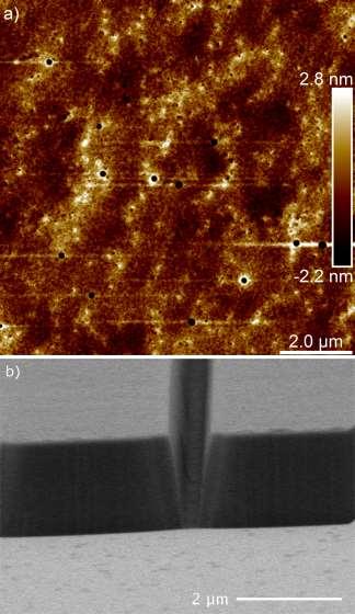
12 An SiO 2 interlayer may be required to protect from metal contamination. In order to keep the SiO 2 as part of the hard mask process, a BCl 3 pre-etch similar to that used by Nedy et al. 14 was developed to clean the GaN surface before the Cl 2 /Ar etch, but after the CHF3 etching of the oxide. The pre-etch conditions used were 10 sccm of BCl 3 at 1.33 Pa with ICP power of 200 W, RF power of 40 W, for 6 minutes. This was found to be sufficient to prevent the micro-masking that led to pillar formation. Figure 9 shows an SEM micrograph of the etch using an SiO 2 /Ti/Ni hard mask leading to 1.07 nm roughness and 13.2 o sidewall angle from vertical. In addition, Figure 10 shows the final etch using SPR as the mask, also utilizing the pre-etch for only 100 seconds. This etch had an angle of 7.6 o, with rms roughness of nm at an etch rate of nm/min. Throughout the study, it was found that using a photoresist mask consistently improved the verticality of the etch over the use of a hard mask. Measurements of the patterned resist gave resist angles of 2.5 o from vertical and an etch rate of about 400 nm/min, twice that of the GaN. In comparison the nickel has been measured to have an etch selectivity of 1:30 with respect to GaN. 12
13 13

14 D. Photoluminescence and Post-Etch In order to evaluate crystal damage near the surface, photoluminescence measurements were performed on samples before and after etching. In addition, some samples were subjected to a very low power BCl 3 /Cl 2 post-etch of varying times. Bias and source powers of 15 W and 50 W respectively were used with flow rates of 20 sccm and 5 sccm for BCl 3 and Cl 2 respectively at 2 Pa. An etch rate of approximately 10 nm/min was measured. This post-etch was intended to remove damaged material without 14
15 causing more damage. By varying the post-etch depths, the depth of the damage from the Cl 2 /Ar etch should be able to be determined. To measure photoluminescence, a 325 nm wavelength HeCd laser with a penetration depth of about 995 Å 9 was used to excite the states near the surface of the GaN. However, when this was done, the post-etch decreased the PL intensity significantly more than the Cl 2 /Ar etch alone. Figure 11 shows that the GaN peak decreases by 32% after the Cl 2 /Ar etch, and an additional 23-39% more so with the postetch. This gives evidence that the Cl 2 /Ar etch causes less damage to the crystal near the surface than the low power BCl 3 /Cl 2 etch per time. The decrease in photoluminescence intensity due to the Cl 2 /Ar etch is much less than that of the BCl 3 /Cl 2 etch described by Qui et al. 12 Further investigation is required to determine the electrical properties of the etched GaN, as well as the sidewalls. 15
16 IV. CONCLUSION An investigation of the effect of the etch parameters for a Cl 2 /Ar etch has been performed. The etch parameters have been adjusted to obtain low roughness and low damage to the crystal while simultaneously achieving sidewalls less than 15 o from vertical. Etches with higher power resulted in enhanced pit formation, whereas etches with lower power resulted in ridge and hill features. The induced etch pillars have been confirmed to result from using SiO 2 in contact with the GaN as part of the hard mask have been observed and has been mitigated with a BCl 3 pre-etch. The use of photoresist as a mask resulted in more vertical sidewalls than using an SiO 2 /Ti/Ni hard mask. The optimized vertical etch gave 7.6 o sidewall angle from vertical with nm surface roughness for a depth of 2 μm at a rate of nm/min. Photoluminescence measurements indicate that there is little damage to the crystal from the etch. ACKNOWLEDGMENTS This work was funded by the Advanced Research Projects Agency Energy for the SWITCHES program. Much of the work was performed at the Nanotech nanofabrication facility at UCSB. 1 Z. Li and P. Chow, "Design and Simulation of 5 20-kV GaN Enhancement-Mode Vertical Superjunction HEMT," IEEE T. Electron Dev., 60, 3230, (2013). 2 R. Yeluri, J. Lu, C. A. Hurni, D. A. Browne, S. Chowdhury, S. Keller, J. S. Speck and U. K. Mishra, Appl. Phys. Lett., 106, , (2015). 16
17 3 H. Otake, K. Chikamatsu, A. Yamaguchi, T. Fujishima and H. Ohta, Appl. Phys. Express, 1, , (2008). 4 S. Chowdhury, B. L. Swenson and U. K. Mishra, IEEE Electr. Device L., 29, 543, (2008). 5 T. Oka, Y. Ueno, T. Ina and K. Hasegawa, Appl. Phys. Express, 7, , (2014). 6 D. A. Stocker, E. F. Schubert and J. M. Redwing, Appl. Phys. Lett., 73, 2654, (1998). 7 Y. H. Im, J. S. Park, K. S. Nahm, Y.-.. S. Lee, B. C. Cho, K. Y. Lim, H. J. Lee and S. J. Pearton, J. Vac. Sci. Technol. A, 18, 2169, (2000). 8 J.-M. Lee, K.-M. Chang, I.-H. Lee and S.-J. Park, J. Electrochem. Soc., 147, 1859, (2000). 9 E. D. Haberer, C.-H. Chen, A. Abare, M. Hansen, S. Denbaars, L. Coldren, U. Mishra and E. L. Hu, Appl. Phys. Lett., 76, 3941, (2000). 10 E. D. Haberer, C. H. Chen, M. Hansen, S. Keller, S. P. Denbaars, U. K. Mishra and E. L. Hu, J. Vac. Sci. Technol. B, 19, 603, (2001). 11 Y. B. Hahn, Y. H. Im, J. S. Park, K. S. Nahm and Y. S. Lee, J. Vac. Sci. Technol. A, 19, 1277, (2001). 12 R. Qiu, H. Lu, D. Chen, R. Zhang and Y. Zheng, Appl. Surf. Sci., 257, 2700, (2010). 13 H. Hahn, J. B. Gruis, N. Ketteniss, F. Urbain, H. Kalisch and A. Vescan, J. Vac. Sci. Technol. A, 30, , (2012). 14 J. G. Nedy, N. G. Young, K. M. Kelchner, Y. Hu, R. M. Farrel, S. Nakamura, S. Denbaars, C. Weisbuch, J. S. Speck, Semicond. Sci. and Tech., 30, , (2015). 15 H. N. Cho, S. R. Min, H. J. Bae, J. H. Lee and C. W. Chung, J. Ind. Eng. Chem., 13, 939, (2007). 17
18 FIG. 1. (Color online) Comparison of roughness and etch rate for increasing ICP source power. Note that the RF bias power is set to 25% of the source power. The roughness presented here is calculated from 2 μm x 2 μm AFM scans. FIG. 2. (Color online) 2 μm x 2 μm AFMs showing the surface features of the lateral etched regions for the various powers tested. FIG. 3. (Color online) a-c) 10 μm x 10 μm AFM scans of flow rate variation series. d-f) SEMs of the same samples. FIG. 4. (Color online) Comparison of pit dimensions and roughness for varying total flow rate. The ratio between Cl 2 and Ar was kept constant at 1:1. FIG. 5. (Color online) a-b) 10 μm x 10 μm AFM scans of gas composition variations. c-d) SEMs of the same samples. FIG. 6. (Color online) Comparison of pit dimensions and roughness for varying pressure. FIG. 7. (Color online) 10 μm x 10 μm AFM scans of pressure variations. FIG. 8. SEM images of pillars formed during the etch when a mask with SiO 2 contacting GaN is used. FIG. 9. (Color online) AFM and SEM of sample etched with an SiO 2 /Ti/Ni hard mask using an optimized Cl 2 /Ar etch with a BCl 3 pre-etch. FIG. 10. (Color online) AFM and SEM of sample etched with an SPR photoresist mask using an optimized Cl 2 /Ar etch with a BCl 3 pre-etch. FIG. 11. (Color online) Comparison of photoluminescence of Cl 2 /Ar etched samples with different post-etch times and an unetched sample as a reference. The peak value of the GaN peak at 365 nm was used to calculate the PL change. 18