Atmospheric Pressure Plasma Technology For Ultra-Precision Engineering Of Optics For Applications In Aerospace, Defence And Science.
|
|
|
- Sherilyn Booker
- 5 years ago
- Views:
Transcription
1 Atmospheric Pressure Plasma Technology For Ultra-Precision Engineering Of Optics For Applications In Aerospace, Defence And Science Adam Bennett
2 Adam Bennett Military Officer First Degree Physics Post Graduate Masters Nanotechnology: First Class Equivalent Highest Grade On The Programme Post Graduate Certificate Ultra Precision Engineering PhD in Ultra Precision Engineering: Plasma (submission April 2018)
3 Aim Applications Background Plasma Figuring Machines Microwave Induced Plasma Systems Characterisation Method Developed Plasma Processing of Optics


4 Microwave Plasma Energy Beam 100mm by 100mm Optics Crystal Quartz Aim Material Removal Rate of 0.1mm 3 /min Form accuracy < 10nm RMS Surface texture < 1nm RMS Applications Acousto-Optics: Beam Deflectors, Frequency Shifters, Modulators, Q Switches Focusing Lens Optic 700mm processing <30nm RMS roughness I) I) II) I) T. Fellers, M. Davidson, 2009, Acousto-Optic Tunable Filters, Report for the National High Magnetic Field Laboratory, USA II) Acousto-Optic, 21/04/2015


5 Other Applications Fusion Energy Research: Using Metre Scale Optics to Focus High Power Laser Beams Focusing Lens Optic 700mm processing <30nm RMS roughness III) Cold Fusion, 21/04/2015
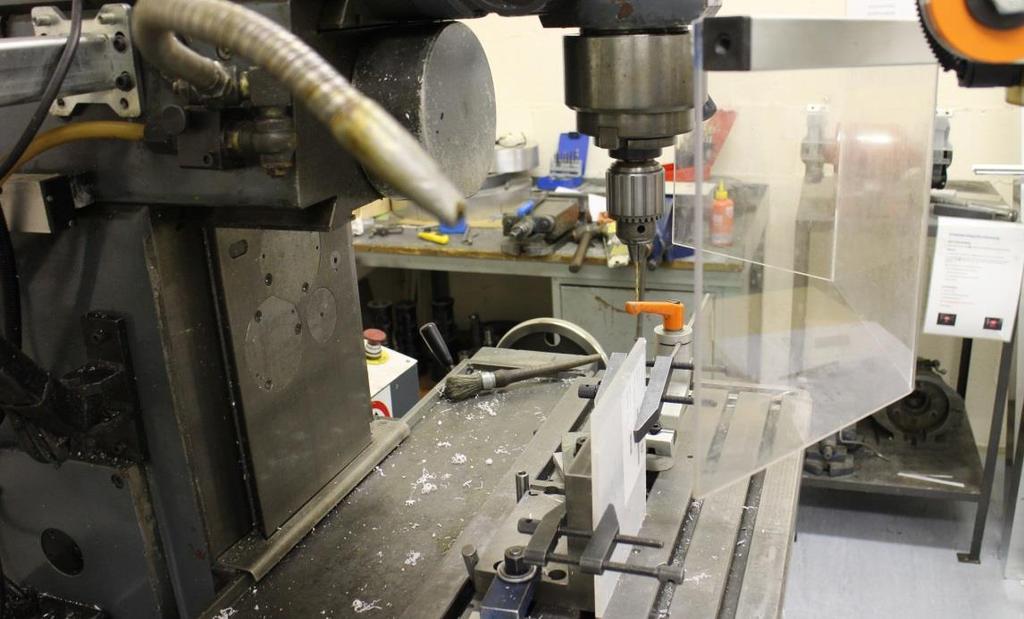
 Polishing machine (Robot) Helios1200 (Plasma figuring")
6 Ultra Precision Surface Processing Route for Large Optics Metre scale optical component Stage 1 Stage 2 Stage 3 Surface roughness < 1 nm RMS Grinding process 1 mm form accuracy 1 μm form accuracy Polishing process 300nm form accuracy Plasma process 10 nm form accuracy BoX (Ultra precision grinding) Polishing machine (Robot) Helios1200 (Plasma figuring machine)


7 Plasma Figuring Machines at Cranfield University RAP Plasma Figuring Machine 300mm x 300mm optical substrate processing capability Atmospheric Pressure Plasma Figuring Helios Plasma Figuring Machine 1200mm x 1200mm optical substrate processing capability Both plasma figuring machines currently employ an Inductively Coupled Plasma torch
8 Microwave Induced Plasma Systems Coaxial Electrode System Surface Wave Launcher System TE f = TM f TE f TM f


9 50W to 200W Surface Wave Launcher System Coaxial Electrode System 13W to 17W 2.4GHz to 2.5GHz Carrier Reactive Gases Gases Argon SF6 Helium CF4
10 Coaxial Electrode Microwave Induced Plasma Torch Transverse Electric frequency = Transverse Magnetic frequency


11 Coaxial Electrode Microwave Induced Plasma Torch Military Microwave Anechoic Chamber Receiving antenna Adtec torch placed into RADAR/MWDAR Anechoic Chamber Anritsu MS spectrum analyser

12 Coaxial Electrode Microwave Induced Plasma Torch Military Microwave Anechoic Chamber
 Angle (Degrees)")
13 Angle (Degrees) Coaxial Electrode Microwave Induced Plasma Torch Directionality of the Microwave Energy being Emitted from the Adtec Electrode Intensity (db) Angle (Degrees)


14 Coaxial Electrode Microwave Induced Plasma Torch Characterisation by Optical Emission Spectroscopy Experimental Setup


15 Δz = 10µm Intensity (Counts) Coaxial Electrode Microwave Induced Plasma Torch Optical Emission Spectroscopy Frequency = 2.45GHz Power = 15W Main Gas Flow = 1L/min Nozzle Gas Flow = 0.01L/min 5000 Spatial resolution = 10µm Each measurement records wavelengths from 400nm to 850nm Wavelength (nm) Δx = 10µm Lens Connected To Spectrometer


16 5mm Coaxial Electrode Microwave Induced Plasma Torch Optical Emission Spectroscopy Results Power = 15W; Frequency = 2.45GHz; Main Gas Flow = 1L/min; Nozzle Gas Flow = 0.01L/min Helium Argon Argon + Argon Argon + SF6 Argon + CF4 2mm 2mm 2mm 2mm 2mm Intensity


17 Previous Plasma Processing Results RMS: 373 nm PVr: 2260 nm Initial figure error RMS: 30nm PVr: 250 nm X3 X2

18 Surface Wave Launched Microwave Induced Plasma Torch TE f TM f


19 Microwave Plasma System & Enclosure Installation

20 Microwave Plasma System & Enclosure Installation


21 Microwave Plasma System & Enclosure Installation


22 Microwave Plasma System & Enclosure Installation

23 Microwave Plasma System & Enclosure Installation
; radio-waves; micro-waves; and reactive atoms.")
24 Plasma Processing The Surface Wave Launcher Microwave Induced Plasma torch was placed into a bespoke enclosure within a Plasma Figuring machine. Contains all UV(UV-A, UV-B, UV-C); radio-waves; micro-waves; and reactive atoms. Enables rapid processing at atmospheric pressure.
; radio-waves; micro-waves; and reactive atoms. Main Gas Flow = 4L/min to 10L/min Main Gas : Reactive Gas = 99.5% : 0.")
25 Plasma Processing The Surface Wave Launcher Microwave Induced Plasma torch was placed into a bespoke enclosure within a Plasma Figuring machine. Frequency = 2.4GHz to 2.5GHz Power = 100W to 200W Contains all UV(UV-A, UV-B, UV-C); radio-waves; micro-waves; and reactive atoms. Main Gas Flow = 4L/min to 10L/min Main Gas : Reactive Gas = 99.5% : 0.5% to 96% : 4% Enables rapid processing at atmospheric pressure. Tool path: the route the torch moves with respect to the optic TE f TM f
 25W 5L/min Ar;")

26 Plasma Processing Plasma Jets: (a) 25W 5L/min Ar; (b) 100W 5L/min Ar; (c) 200W 5L/min Ar. (a) (b) (c)


27 Plasma Processing Stationary Dwell Material Removal

28 Plasma Processing Stationary Dwell Material Removal Power = 100W, Frequency = 2.45GHz, Main Gas Flow = 5L/min, Reactive Gas Flow = 10% CF4 in 0.5L/min, Stand-Off Distance = 10mm, Dwell Time = 10s Optical Substrate = ULE FWHM = 2mm
29 Plasma Processing Stationary Dwell Material Removal Power effect on maximum depth

30 Plasma Processing Single Trench Material Removal


31 Plasma Processing Single Trench Material Removal Power = 150W, Frequency = 2.45GHz, Main Gas Flow = 5L/min, Reactive Gas Flow = 10% CF4 in 0.5L/min, Stand-Off Distance = 10mm, Optical Substrate = ULE FWHM = 2mm Torch Speed = 10mm/min


32 Surface Wave Launched Microwave Induced Plasma Torch Characterisation by Optical Emission Spectroscopy Experimental Setup


33 nm Plasma Processing Surface Figuring Material Removal Crystal Quartz Surface Roughness Form Correction Capability

34 Plasma Processing Stationary Dwell Material Deposition
35 Summary Novel Microwave Spectrum & Optical Emission Spectroscopy techniques developed to characterise plasma torches. New microwave plasma system has been commissioned and installed into the plasma figuring machine. Stable material removal on the surface of optics has been demonstrated. Full Design Of Experiments conducted to optimise the parameters. Entire surface of Crystal Quartz substrates have been processed. Deposition has also been demonstrated!
36 Acknowledgements Cranfield University EPSRC Centre for Innovative Manufacturing in Ultra Precision {EP/I033491/1}: Plasma Figuring Laboratory University Of Cambridge EPSRC Centre for Doctoral Training in Ultra Precision {EP/K503241/1}: Project Funding Gooch & Housego: Project Funding ADTEC: Technical Support & Pioneering Microwave Plasma System Loan Defence Academy: Military Grade Microwave Characterisation

37 Adam Bennett Doctoral Research Scientist EPSRC Centre for Doctoral Training in Ultra Precision EPSRC Centre for Innovative Manufacturing in Ultra Precision