Evaluation of Cu Pillar Chemistries
|
|
|
- Shanna Walton
- 6 years ago
- Views:
Transcription


1 Presented at 2016 IMAPS Device Packaging Evaluation of Cu Pillar Chemistries imaps Device Packaging Conference Spring 2016 Matthew Thorseth, Mark Scalisi, Inho Lee, Sang-Min Park, Yil-Hak Lee, Jonathan Prange, Masaaki Imanari, Mark Lefebvre, Jeff Calvert Dow.com
2 Outline Introduction Cu Pillar Plating with INTERVIA Cu Products RDL Pillars Solder integration Next generation performance Megapillars 50 μm pillars

3 Background and Introduction SnAg Solder plating SOLDERON BP TS 4000 SnAg SOLDERON BP TS 6000 SnAg ETNA 3D chip stack with DRAM and Logic integration SnAg C4 Bump Cu Through-Si Via INTERLINK 9200 Cu Redistribution Layer Cu INTERVIA 8540 Cu INTERVIA 9000 Cu Cu pillar INTERVIA 8540 Cu INTERVIA 9000 Cu Memory Image courtesy of IMEC Logic Dual Damascene Cu ULTRAFILL 5001 Cu NANOPLATE 5200 Cu Ni Barrier Layer NIKAL BP Ni NIKAL BP 2000 Ni Solders Used for electrical joint formation, previously had been SnPb, shift to SnAg due to environmental concerns Copper Conductor used to carry signals throughout the chip package Nickel Used mainly as a seed & barrier layer to prevent intermetallic mixing at metal/metal interfaces 3
4 Background and Introduction Technology Trend in Packaging SnPb C4 Bump Pb-Free C4 Bump Cu Pillar + Pb-free Cap Cu µ-pillar + Pb-free Cap Structure SnAg SnAg Cu SnAg Cu Diameter µm µm µm µm Products SOLDERON BP + NIKAL BP Ni NIKAL BP 2000 Ni SOLDERON BP TS 4000 SnAg SOLDERON BP TS 6000 SnAg + NIKAL BP Ni NIKAL BP 2000 Ni INTERVIA 8540 Cu INTERVIA 9000 Cu + NIKAL BP Ni NIKAL BP 2000 Ni + SOLDERON Products INTERVIA Cu Products + NIKAL Products + SOLDERON Products Old Technology Current Technology Next-Generation Technology 4
5 Process Flow and Design Goals Incoming Wafer PR Si Seed Layer Passivation UBM Electroplating SnAg Ni Cu PR Strip, Seed Layer Etch, Reflow Design Goal RDL Target 20 μm Pillar Target 50 μm Pillar Target %WID Uniformity < 5% < 5% < 5% < 10% 200 μm Pillar Target %TIR Doming -5% to 5% -5% to 5% -5% to 5% -5% to 5% Plating Rate 2 to 12 ASD 4.5 to 12 ASD 4.5 to 18 ASD 20 to 40 ASD Total Doping (C,N,O,S,Cl) Solder Compatibility Void-free w/o Ni Barrier < 20 ppm < 20 ppm < 20 ppm < 20 ppm Void-free w/o Ni Barrier Void-free w/o Ni Barrier Void-free w/o Ni Barrier 5

 Height Center")
 Flat (0")
6 Definitions Height Max Within-die (WID) Co-planarity Height Min 1 Height Max Height Min % WID Height Avg Total Indicated Runout (TIR) Height Center Height Edge Height Center Height Edge % TIR 100 Height Max Dished (-TIR) Flat (0 TIR) Domed (+TIR) 6
7 300 mm Data INTERVIA Copper Chemistry


8 Redistribution Layer Pattern Plating at 4.5 ASD IV8540 INTERVIA 8540 Cu Images INTERVIA 9000 Cu Images Feature Size Optical Image Profile Optical Image Profile 5/5 μm line/space comb 50/50 μm line/space comb 100 μm square pad Similar plating performances between chemistries, with slightly less domed profiles with INTERVIA 9000 Cu 50 μm bond pad with 10 μm lines 8


9 Pillar Plating Performance Across Feature Sizes INTERVIA 8540 Cu Images INTERVIA 9000 Cu Images Pillar Size and Plating Rate Optical Image Profile Pillar Size and Plating Rate Optical Image Profile 20 μm pillar at 8 ASD 20 μm pillar at 8 ASD 50 μm pillar at 14 ASD 50 μm pillar at 14 ASD 75 μm pillar at 14 ASD 75 μm pillar at 14 ASD INTERVIA 9000 Cu pillars have lower doming across all pillar types 9

10 %WID 40 μm Pitch %TIR 40 μm Pitch INTERVIA 8540 Cu vs. INTERVIA 9000 Cu 20 μm diameter micropillars 20% 15% INTERVIA 8540 INTERVIA 9000 INTERVIA Cu 8540 Images INTERVIA Cu 9000 Images 10% 5% Current Density / ASD Optical Image Profile Dense Pitch Current Density / ASD Optical Image Profile Dense Pitch 0% Current Density / ASD 10% INTERVIA 8540 INTERVIA % 0% Current Density / ASD 10
11 %WID 100 μm Pitch %TIR 100 μm Pitch INTERVIA 8540 vs. INTERVIA μm diameter pillars 20% 15% INTERVIA 8540 INTERVIA 9000 INTERVIA 8540 Images INTERVIA 9000 Images 10% 5% Current Density / ASD Optical Image Profile Dense Pitch Current Density / ASD Optical Image Profile Dense Pitch 0% -5% Current Density / ASD % INTERVIA % INTERVIA % % 10% 5% 0% Current Density / ASD 11


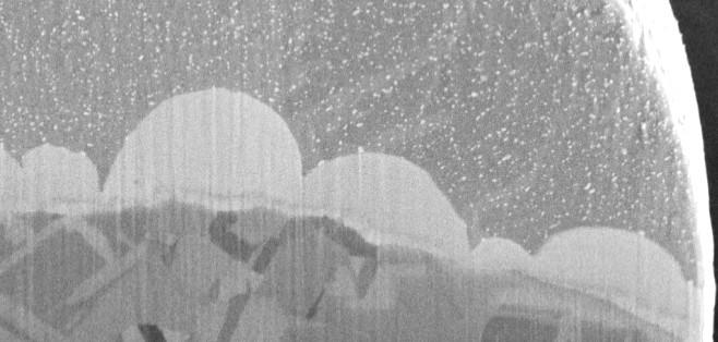
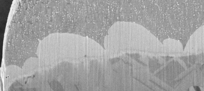
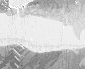
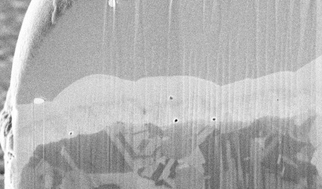
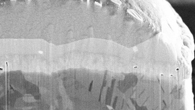
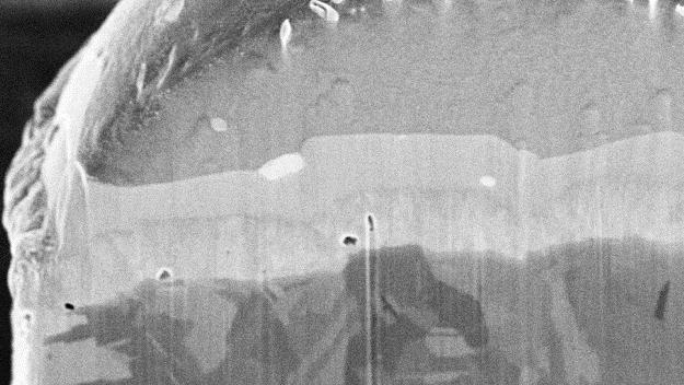
12 INTERVIA Cu Megapillar Plating Segment Level INTERVIA 8540 Cu INTERVIA 9000 Cu 18.5 ASD Avg. Plating Rate WID = 3.5% TIR > 10.3% WID = 4.0% TIR = 5.0% 12


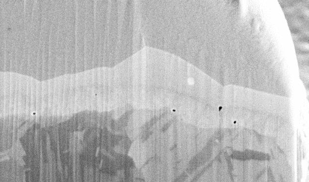
13 Solder Integration with INTERVIA Cu on 20 μm Pillars INTERVIA 8540 Cu 1 Reflow INTERVIA 9000 Cu 10 Reflows High Temperature Storage at 150 C for 125 hr. Minimal voiding at SnAg-Cu interface after multiple reflows and HTS 13


 of <20 ppm as measured by SIMS")
14 INTERVIA 9000 Cu Integration with Ni and SnAg 20 µm Ø Pillar, 9 ASD, 1x Reflow 50 µm Ø Pillar, 9 ASD, 1x Reflow Solderon BP TS 6000 SnAg Solderon BP TS 6000 SnAg NIKAL BP Ni Solderon BP TS 6000 SnAg Solderon BP TS 6000 SnAg NIKAL BP Ni INTERVIA 9000 INTERVIA 9000 INTERVIA 9000 INTERVIA 9000 w/o Ni w/ 2 µm Ni w/o Ni w/ 2 µm Ni Excellent Compatibility with NIKAL BP Nickel and SOLDERON BP TS 6000 Tin- Silver in both 20 um and 50 um Ø sizes Organic doping (C, O, N, S, Cl) of <20 ppm as measured by SIMS 14
15 INTERVIA Cu Deposit Summary INTERVIA 8540 and 9000 Copper Chemistry deposits have excellent WID uniformity with superior integration with solder materials Both plating baths deposit pure Cu across a wide range of applications, including RDL, micropillar, pillar, and megapillars INTERVIA 9000 Cu deposits are flatter than INTERVIA 8540 Cu Plating rates of at least 18 ASD (4 μm min -1 ) are achievable with INTERVIA 9000 Cu plating baths Both chemistries deposit Cu with robust Cu-solder interfaces with minimal interfacial voiding, even after HTS at 150 C 15
16 Next Generation Prototype Chemistries Segment Level Testing


17 %Spec Total Organic Incorporation 200 μm Megapillar Prototype Chemistry 1 Plating Rate / ASD ASD 10% 5% %WID %TIR High Speed Cu Prototype INTERVIA 9000 INTERVIA % Plating Rate / ASD Plating Rate / ASD High purity deposits with both INTERVIA 9000 Cu and new prototype chemistry at plating rates up to 40 ASD Uniform grain size without voiding up to 40 ASD 17


18 %WID %TIR 50 μm Pillar Prototype Chemistry 2 Plating Rate / ASD Optical Images INTERVIA 9000 Cu Prototype Chemistry 15% 10% 5% 0% INTERVIA 9000 Prototype % 50% Plating Rate / ASD INTERVIA 9000 Prototype Similar TIR flat TIR performance in new prototype chemistry to INTERVIA 9000 Cu Significant improvement in WID at high plating rates with new prototype 25% 0% Plating Rate / ASD 18
19 Thank You Trademark of the Dow Chemical Company ( Dow ) or an affiliated company of Dow
MEPTEC Semiconductor Packaging Technology Symposium
 MEPTEC Semiconductor Packaging Technology Symposium Advanced Packaging s Interconnect Technology Process Shift and Direction October 23, 2014 Jay Hayes- Director of Business Development -Bumping and Flip
Cu electroplating in advanced packaging
 Cu electroplating in advanced packaging March 12 2019 Richard Hollman PhD Principal Process Engineer Internal Use Only Advancements in package technology The role of electroplating Examples: 4 challenging
SLIM TM, High Density Wafer Level Fan-out Package Development with Submicron RDL
 2017 IEEE 67th Electronic Components and Technology Conference SLIM TM, High Density Wafer Level Fan-out Package Development with Submicron RDL YoungRae Kim 1, JaeHun Bae 1, MinHwa Chang 1, AhRa Jo 1,
Optimized Cu plating in fan-out wafer-level packaging MultiPlate: a turnkey solution
 Optimized Cu plating in fan-out wafer-level packaging MultiPlate: a turnkey solution Cassandra Melvin Global Product Manager, Advanced Packaging Outline 1. Global megatrend IoT 2. Fan-out wafer-level packaging
TSV Interposer Process Flow with IME 300mm Facilities
 TSV Interposer Process Flow with IME 300mm Facilities Property of Institute of Microelectronics (IME)-Singapore August 17, 2012 Outline 1. TSV interposer (TSI) cross sectional schematic TSI with BEOL,
Lead-Free Solder Bump Technologies for Flip-Chip Packaging Applications
 Lead-Free Solder Bump Technologies for Flip-Chip Packaging Applications Zaheed S. Karim 1 and Jim Martin 2 1 Advanced Interconnect Technology Ltd. 1901 Sunley Centre, 9 Wing Yin Street, Tsuen Wan, Hong
Enabling Materials Technology for Multi-Die Integration
 Enabling Materials Technology for Multi-Die Integration Dr. Jeffrey M. Calvert Global R&D Director, Advanced Packaging Technologies Dow Electronic Materials 455 Forest St., Marlborough, MA 01752 USA jcalvert@dow.com
Ultra Fine Pitch Bumping Using e-ni/au and Sn Lift-Off Processes
 Ultra Fine Pitch Bumping Using e-ni/au and Sn Lift-Off Processes Andrew Strandjord, Thorsten Teutsch, and Jing Li Pac Tech USA Packaging Technologies, Inc. Santa Clara, CA USA 95050 Thomas Oppert, and
Fraunhofer IZM Bump Bonding and Electronic Packaging
 Fraunhofer IZM Bump Bonding and Electronic Packaging Fraunhofer Institute for Reliability and Microintegration (IZM) Gustav-Meyer-Allee 25 13355 Berlin Germany Dipl.-Ing. Thomas Fritzsch Contact: thomas.fritzsch@izm.fraunhofer.de
Chips Face-up Panelization Approach For Fan-out Packaging
 Chips Face-up Panelization Approach For Fan-out Packaging Oct. 15, 2015 B. Rogers, D. Sanchez, C. Bishop, C. Sandstrom, C. Scanlan, TOlson T. REV A Background on FOWLP Fan-Out Wafer Level Packaging o Chips
TSV Processing and Wafer Stacking. Kathy Cook and Maggie Zoberbier, 3D Business Development
 TSV Processing and Wafer Stacking Kathy Cook and Maggie Zoberbier, 3D Business Development Outline Why 3D Integration? TSV Process Variations Lithography Process Results Stacking Technology Wafer Bonding
3DIC Integration with TSV Current Progress and Future Outlook
 3DIC Integration with TSV Current Progress and Future Outlook Shan Gao, Dim-Lee Kwong Institute of Microelectronics, A*STAR (Agency for Science, Technology and Research) Singapore 9 September, 2010 1 Overview
Electrical and Fluidic Microbumps and Interconnects for 3D-IC and Silicon Interposer
 Electrical and Fluidic Microbumps and Interconnects for 3D-IC and Silicon Interposer Li Zheng, Student Member, IEEE, and Muhannad S. Bakir, Senior Member, IEEE Georgia Institute of Technology Atlanta,
TIN-BASED LEAD-FREE SOLDER BUMPS FOR FLIP-CHIP APPLICATION. S. Yaakup, H. S. Zakaria, M. A. Hashim and A. Isnin
 TIN-BASED LEAD-FREE SOLDER BUMPS FOR FLIP-CHIP APPLICATION S. Yaakup, H. S. Zakaria, M. A. Hashim and A. Isnin Advanced Materials Research Centre (AMREC), SIRIM Berhad, Lot 34, Jalan Hi-Tech 2/3, Kulim
UTILIZATION OF ATMOSPHERIC PLASMA SURFACE PREPARATION TO IMPROVE COPPER PLATING PROCESSES.
 SESSION 14 MATERIALS AND PROCESSES FOR ADVANCED PACKAGING UTILIZATION OF ATMOSPHERIC PLASMA SURFACE PREPARATION TO IMPROVE COPPER PLATING PROCESSES. Eric Schulte 1, Gilbert Lecarpentier 2 SETNA Corporation
Thermo-Mechanical Reliability of Through-Silicon Vias (TSVs)
") 1 Thermo-Mechanical Reliability of Through-Silicon Vias (TSVs) Xi Liu Ph.D. Student and Suresh K. Sitaraman, Ph.D. Professor The George W. Woodruff School of Mechanical Engineering Georgia Institute of
1 Thermo-Mechanical Reliability of Through-Silicon Vias (TSVs) Xi Liu Ph.D. Student and Suresh K. Sitaraman, Ph.D. Professor The George W. Woodruff School of Mechanical Engineering Georgia Institute of
Supplementary Materials for
 www.sciencemag.org/cgi/content/full/336/6084/1007/dc1 Supplementary Materials for Unidirectional Growth of Microbumps on (111)-Oriented and Nanotwinned Copper Hsiang-Yao Hsiao, Chien-Min Liu, Han-wen Lin,
S/C Packaging Assembly Challenges Using Organic Substrate Technology
 S/C Packaging Assembly Challenges Using Organic Substrate Technology Presented by Bernd Appelt ASE Group Nov. 17, 2009 Overview The Packaging Challenge Chip Substrate Interactions Stiffeners for FC-BGA
Flip Chip Bump Electromigration Reliability: A comparison of Cu Pillar, High Pb, SnAg, and SnPb Bump Structures
 Flip Chip Bump Electromigration Reliability: A comparison of Cu Pillar,,, and SnPb Bump Structures Ahmer Syed, Karthikeyan Dhandapani, Lou Nicholls, Robert Moody, CJ Berry, and Robert Darveaux Amkor Technology
SEMI Networking Day 2013 Rudolph Corporate Introduction
 SEMI Networking Day 2013 Rudolph Corporate Introduction Rudolph Technologies: Corporate Profile Business: Semiconductor capital equipment company dedicated exclusively to inspection, advanced packaging
3D Package Technologies Review with Gap Analysis for Mobile Application Requirements. Apr 22, 2014 STATS ChipPAC Japan
 3D Package Technologies Review with Gap Analysis for Mobile Application Requirements Apr 22, 2014 STATS ChipPAC Japan T.Nishio Contents Package trends and roadmap update Advanced technology update Fine
Notable Trends in CMP: Past, Present and Future
 Notable Trends in CMP: Past, Present and Future Semiconductor International February 15 th, 2007 Pete Singer Editor-in-Chief Levitronix CMP Users Conference 2007 April 1988: Etchback, SOG November 1990:
Innovative Substrate Technologies in the Era of IoTs
 Innovative Substrate Technologies in the Era of IoTs Dyi- Chung Hu 胡迪群 September 4, 2015 Unimicron Contents Introduction Substrate Technology - Evolution Substrate Technology - Revolution Glass substrate
Interconnect Structure for Room Temperature 3D-IC Stacking Employing Binary Alloying for High Temperature Stability
 Minapad 2014, May 21 22th, Grenoble; France Interconnect Structure for Room Temperature 3D-IC Stacking Employing Binary Alloying for High Temperature Stability Eric Schulte 1, Keith Cooper 1 Matthew Lueck
Simulations and Characterizations for Stress Reduction Designs in Wafer Level Chip Scale Packages
 Simulations and Characterizations for Stress Reduction Designs in Wafer Level Chip Scale Packages by Ming-Che Hsieh STATS ChipPAC Taiwan Co. Ltd. Copyright 2013. Reprinted from 2013 International Microsystems,
RoHS Compliance Document
 D2-Pak RoHS Compliance Document Contents: 1. 2. Solder Reflow 3. Tin Whisker Report D2-pak (3 or 5 Lead) BOM 1 90598-46-2 0.05808 11% 3.8% Lead Frame Copper 0.94840 Die Attach Soft Solder 0.01200 Cu 7440-50-8
Reaction of Sn-Bearing Solders with Nickel-based Under Bump Metallisations
 STR/03/069/ST Reaction of Sn-Bearing Solders with Nickel-based Under Bump Metallisations G. Qi, M. He and Z. Chen Abstract This work relates to wafer bumping technologies for flip chip packaging applications
1 mw/[] Bond-Able Post-Passivation Interconnect for Power Management Technologies.
![1 mw/[] Bond-Able Post-Passivation Interconnect for Power Management Technologies.](/thumbs/96/129184811.jpg "1 mw/[] Bond-Able Post-Passivation Interconnect for Power Management Technologies.") 1 mw/[] Bond-Able Post-Passivation Interconnect for Power Management Technologies. Alexander Kalnitsky, Y.W. Tseng, T.H. Chien, C.Y. Chang, Felix Tsui 1 Outline Technology development Planarized passivation
1 mw/[] Bond-Able Post-Passivation Interconnect for Power Management Technologies. Alexander Kalnitsky, Y.W. Tseng, T.H. Chien, C.Y. Chang, Felix Tsui 1 Outline Technology development Planarized passivation
Properties and Barrier Material Interactions of Electroless Copper used for Seed Enhancement
 Mat. Res. Soc. Symp. Proc. Vol. 766 2003 Materials Research Society E1.4.1 Properties and Barrier Material Interactions of Electroless Copper used for Seed Enhancement C. Witt a,b,k.pfeifer a,c a International
Probing Challenges with Cu Pillar. Phill Mai, JEM America Joe Mai, JEM Europe
 Probing Challenges with Cu Pillar Phill, JEM America Joe, JEM Europe Crown-tip probe limitations MEMS probe with flat tip Summary Future work Overview 2 Crown-to-bump contact Piercing Contact Probe mark
INTERCONNECT STRUCTURE FOR ROOM TEMPERATURE 3D-IC STACKING EMPLOYING BINARY ALLOYING FOR HIGH TEMPERATURE STABILITY
 INTERCONNECT STRUCTURE FOR ROOM TEMPERATURE 3D-IC STACKING EMPLOYING BINARY ALLOYING FOR HIGH TEMPERATURE STABILITY Eric Schulte 1, Matthew Lueck 2, Alan Huffman 2, Chris Gregory 2, Keith Cooper 1, Dorota
An Innovative High Throughput Thermal Compression Bonding Process
 An Innovative High Throughput Thermal Compression Bonding Process Li Ming 2 September 2015 Outline Introduction Throughput improved TCB Process Liquid Phase Contact (LPC) bonding Flux-LPC-TCB under inert
1 Thin-film applications to microelectronic technology
 1 Thin-film applications to microelectronic technology 1.1 Introduction Layered thin-film structures are used in microelectronic, opto-electronic, flat panel display, and electronic packaging technologies.
THE EFFECTS OF PLATING MATERIALS, BOND PAD SIZE AND BOND PAD GEOMETRY ON SOLDER BALL SHEAR STRENGTH
 THE EFFECTS OF PLATING MATERIALS, BOND PAD SIZE AND BOND PAD GEOMETRY ON SOLDER BALL SHEAR STRENGTH Keith Rogers and Craig Hillman CALCE Electronic Products and Systems Center University of Maryland College
Developments in low-temperature metal-based packaging
 Developments in low-temperature metal-based packaging 2011. 12.14 Jiyoung Chang and Liwei Lin Ph.D. Candidate, Department of Mechanical Engineering University of California at Berkeley 1 1 Contents Project
IME Technical Proposal. High Density FOWLP for Mobile Applications. 22 April High Density FOWLP Consortium Forum
 IME Technical Proposal High Density FOWLP for Mobile Applications 22 April 2014 Packaging driver for portable / mobile applications Key drivers/needs Smaller form-factor lower profile, substrate-less Higher
Cu Pillar Interconnect and Chip-Package-Interaction (CPI) for Advanced Cu Low K chip
 for Advanced Cu Low K chip") EPRC 12 Project Proposal Cu Pillar Interconnect and Chip-Package-Interaction (CPI) for Advanced Cu Low K chip 15 th Aug 2012 Page 1 Introduction: Motivation / Challenge Silicon device with ultra low k
EPRC 12 Project Proposal Cu Pillar Interconnect and Chip-Package-Interaction (CPI) for Advanced Cu Low K chip 15 th Aug 2012 Page 1 Introduction: Motivation / Challenge Silicon device with ultra low k
DITF ToolKit 1. Standard Substrate Sizes (selected at the factory for optimum process)
") DITF ToolKit 1 DITF Toolkit Substrates Common Substrate Materials Alumina (99.5% min) єr = 9.9 Tan d = 1.5 x10⁻⁴ Aluminum Nitride (K170) єr = 8.9 Tan d = 2.0 x10⁻³ Beryllia (99.5%) єr = 6.7 Tan d = 3.0
DITF ToolKit 1 DITF Toolkit Substrates Common Substrate Materials Alumina (99.5% min) єr = 9.9 Tan d = 1.5 x10⁻⁴ Aluminum Nitride (K170) єr = 8.9 Tan d = 2.0 x10⁻³ Beryllia (99.5%) єr = 6.7 Tan d = 3.0
Overview of CMP for TSV Applications. Robert L. Rhoades, Ph.D. Presentation for AVS Joint Meeting June 2013 San Jose, CA
 Overview of CMP for TSV Applications Robert L. Rhoades, Ph.D. Presentation for AVS Joint Meeting June 2013 San Jose, CA Outline TSV s and the Role of CMP TSV Pattern and Fill TSV Reveal (non-selective)
RoHS Compliance Document
 D-Pak RoHS Compliance Document Contents: 1. 2. Solder Reflow 3. Tin Whisker Report D-pak BOM 1 Chip Silicon.713 Si 744-21-3.713 1% 1.9% Encapsulant Epoxy Resin.11419 Lead Frame Copper.244 Die Attach Soft
Equipment and Process Challenges for the Advanced Packaging Landscape
 Equipment and Process Challenges for the Advanced Packaging Landscape Veeco Precision Surface Processing Laura Mauer June 2018 1 Copyright 2018 Veeco Instruments Inc. Outline» Advanced Packaging Market
Challenges and Solutions for Cost Effective Next Generation Advanced Packaging. H.P. Wirtz, Ph.D. MiNaPAD Conference, Grenoble April 2012
 Challenges and Solutions for Cost Effective Next Generation Advanced Packaging H.P. Wirtz, Ph.D. MiNaPAD Conference, Grenoble April 2012 Outline Next Generation Package Requirements ewlb (Fan-Out Wafer
Adaption to scientific and technical progress under Directive 2002/95/EC
 . Adaption to scientific and technical progress under Directive 2002/95/EC Results previous evaluation Exemption No. 15 Lead in solders to complete a viable electrical connection between semiconductor
By Ron Blankenhorn, Pac Tech USA, Santa Clara, Calif., and Thomas Oppert, Pac Tech GbmH, Nauen, Germany
 INTRODUCTION Modern microelectronic products require packages that address the driving forces of reduced size and weight, as well as increased performance at high frequencies. Flipchip and direct chip
INTERVIA BPP-10 Photoresist
 Technical Data Sheet INTERVIA BPP-10 Photoresist For Advanced Packaging Applications Description Regional Product Availability Advantages INTERVIA BPP-10 Photoresist is a general-purpose, multi-wavelength
Fluxless soldering using Electron Attachment (EA) Technology
 Technology") Fluxless soldering using Electron Attachment (EA) Technology Proprietary, patented innovation for wafer level packaging applications including wafer bump and copper pillar reflow. Air Products has partnered
Fluxless soldering using Electron Attachment (EA) Technology Proprietary, patented innovation for wafer level packaging applications including wafer bump and copper pillar reflow. Air Products has partnered
Adaption to scientific and technical progress under Directive 2002/95/EC
 . Adaption to scientific and technical progress under Directive 2002/95/EC Results previous evaluation Exemption No. 7 a a) Lead in high melting temperature type solders (i.e. lead-based alloys containing
Metallization of MID Dec 2 010
 Metallization of MID Dec 2010 Agenda Introduction to Dow Electronic Materials MID Applications & Advantages Dow MID Metallization Processes Plating Equipment Summary Dow Business Structure Where Dow Electronic
3D technologies for integration of MEMS
 3D technologies for integration of MEMS, Fraunhofer Institute for Electronic Nano Systems Folie 1 Outlook Introduction 3D Processes Process integration Characterization Sample Applications Conclusion Folie
Shear Strength in Solder Bump Joints for High Reliability Photodiode Packages
 Materials Transactions, Vol. 44, No. 10 (2003) pp. 2163 to 2168 #2003 The Japan Institute of Metals Shear Strength in Solder Bump Joints for High Reliability Photodiode Packages Chong-Hee Yu 1, Kyung-Seob
In-line Hybrid Metrology Solutions
 In-line Hybrid Metrology Solutions Brad Lawrence Regional Sales & Product Marketing Manager, XwinSys ED-XRF Based Metrology with Hybrid Sensor Technology Hybrid Sensor In-Line Metrology Process feedback
Thermo-Mechanical FEM Analysis of Lead Free and Lead Containing Solder for Flip Chip Applications
 Thermo-Mechanical FEM Analysis of Lead Free and Lead Containing Solder for Flip Chip Applications M. Gonzalez 1, B. Vandevelde 1, Jan Vanfleteren 2 and D. Manessis 3 1 IMEC, Kapeldreef 75, 3001, Leuven,
Using Mass Metrology for Process Monitoring and Control During 3D Stacking of IC s
 Metryx Copyright 1 Using Mass Metrology for Process Monitoring and Control During 3D Stacking of IC s SEMATECH 3D Interconnect Workshop 11 th July 2012 Metryx Copyright 2 Mass Metrology Less Mass More
Maximum MAX662 12V DC-DC Converter
 Construction Analysis Maximum MAX662 12V DC-DC Converter Report Number: SCA 9512-445 Global Semiconductor Industry the Serving Since 1964 17350 N. Hartford Drive Scottsdale, AZ 85255 Phone: 602-515-9780
Challenges in Material Applications for SiP
 Challenges in Material Applications for SiP Sze PeiLim Regional Product Manager for Semiconductor Products Indium Corporation Indium Corporation Materials Supplier: SMT solder pastes and fluxes Power semiconductor
1.3.2 Nanotechnology Nanoporosity Deposition Methods Dissolution Methods
 Table of Contents 1. Metal Finishing 1 1.1 Introduction 1 1.1.1 Description of Industrial Activity Covered 1 1.1.2 Environmental and Legislative Background 3 1.1.3 Emerging Technology or Research? 4 1.2
28nm Mobile SoC Copper Pillar Probing Study. Jose Horas (Intel Mobile Communications) Amy Leong (MicroProbe) Darko Hulic (Nikad)
 Amy Leong (MicroProbe) Darko Hulic (Nikad)") 28nm Mobile SoC Copper Pillar Probing Study Jose Horas (Intel Mobile Communications) Amy Leong (MicroProbe) Darko Hulic (Nikad) Overview Introduction to IMC Copper Pillar Implementation at IMC Low force
28nm Mobile SoC Copper Pillar Probing Study Jose Horas (Intel Mobile Communications) Amy Leong (MicroProbe) Darko Hulic (Nikad) Overview Introduction to IMC Copper Pillar Implementation at IMC Low force
WF6317. A superactive low-volatile/high heat-resistant water-soluble flux for ball soldering
 WF637 A superactive low-volatile/high heat-resistant water-soluble flux for ball soldering Low viscosity and high tacking power stabilize ball holding force and ensures excellent solder wettability Easy
Bonding Technologies for 3D-Packaging
 Dresden University of Technology / Karsten Meier, Klaus-Juergen Wolter NanoZEIT seminar @ SEMICON Europa 2011 Dresden System integration by SoC or SiP solutions offer advantages regarding design efforts,
RELIABILITY IMPACT OF COPPER-DOPED EUTECTIC TIN-LEAD BUMP AND ITS VOIDING UPON FLIP CHIP ASSEMBLIES
 RELIABILITY IMPACT OF COPPER-DOPED EUTECTIC TIN-LEAD BUMP AND ITS VOIDING UPON FLIP CHIP ASSEMBLIES David Ihms and Shing Yeh Delphi Electronics & Safety Kokomo, IN, USA david.w.ihms@delphi.com and shing.yeh@delphi.com
CHALLENGES FACING ELECTROCHEMICAL DEPOSITION IN WAFER LEVEL PACKAGING MAY THOMAS B. RICHARDSON, Ph.D.
 CHALLENGES FACING ELECTROCHEMICAL DEPOSITION IN WAFER LEVEL PACKAGING MAY 2016 THOMAS B. RICHARDSON, Ph.D. Executive Summary Mobile devices are a leading driver to growth in the IC market, specifically
Flip Chip - Integrated In A Standard SMT Process
 Flip Chip - Integrated In A Standard SMT Process By Wilhelm Prinz von Hessen, Universal Instruments Corporation, Binghamton, NY This paper reviews the implementation of a flip chip product in a typical
Motorola MC68360EM25VC Communication Controller
 Construction Analysis EM25VC Communication Controller Report Number: SCA 9711-562 Global Semiconductor Industry the Serving Since 1964 17350 N. Hartford Drive Scottsdale, AZ 85255 Phone: 602-515-9780 Fax:
CERN/NA62 GigaTracKer Hybrid Module Manufacturing
 CERN/NA62 GigaTracKer Hybrid Module Manufacturing Fraunhofer Institute for Reliability and Microintegration Gustav-Meyer-Allee 25 13355 Berlin Germany Dipl.-Ing. Thomas Fritzsch Contact: Fraunhofer IZM
Ultralow Residue Semiconductor Grade Fluxes for Copper Pillar Flip-Chip
 Ultralow Residue Semiconductor Grade Fluxes for Copper Pillar Flip-Chip SzePei Lim (Presenter), Jason Chou, Maria Durham, and Dr. Andy Mackie Indium Corporation 1 Outline of Presentation Roadmaps and challenges
Advanced Analytical Techniques for Semiconductor Assembly Materials and Processes. Jason Chou and Sze Pei Lim Indium Corporation
 Advanced Analytical Techniques for Semiconductor Assembly Materials and Processes Jason Chou and Sze Pei Lim Indium Corporation Agenda Company introduction Semiconductor assembly roadmap challenges Fine
Investigation of the recommended immersion Tin thickness for Pbfree
 Investigation of the recommended immersion Tin thickness for Pbfree soldering Sven Lamprecht Atotech Deutschland GmbH Berlin Abstract First choices for Pb-free soldering are SnAgCu alloys, which are in
A STUDY OF THE ENEPIG IMC FOR EUTECTIC AND LF SOLDERS
 A STUDY OF THE ENEPIG IMC FOR EUTECTIC AND LF SOLDERS G.Milad, D.Gudeczauskas, G.Obrien, A.Gruenwald Uyemura International Corporation Southington, CT ABSTRACT: The solder joint formed on an ENEPIG surface
A study aimed at characterizing the interfacial structure in a tin silver solder on nickel-coated copper plate during aging
 Sādhanā Vol. 33, Part 3, June 2008, pp. 251 259. Printed in India A study aimed at characterizing the interfacial structure in a tin silver solder on nickel-coated copper plate during aging D C LIN 1,
UMC UM F-7 2M-Bit SRAM
 Construction Analysis UMC UM 613264F-7 2M-Bit SRAM Report Number: SCA 9609-511 Global Semiconductor Industry the Serving Since 1964 15022 N. 75th Street Scottsdale, AZ 85260-2476 Phone: 602-998-9780 Fax:
Challenges of Fan-Out WLP and Solution Alternatives John Almiranez
 Challenges of Fan-Out WLP and Solution Alternatives John Almiranez Advanced Packaging Business Development Asia Introduction to Fan-Out WLP Introduction World of mobile gadgetry continues to rapidly evolve
Method For Stripping Copper In Damascene Interconnects >>>CLICK HERE<<<
 Method For Stripping Copper In Damascene Interconnects Damascene, or acid copper plating baths, have been in use since the mid 19th century on decorative items and machinery.1,2 The process generally uses
Interfacial Reactions between the Sn-9Zn Solder and Au/Ni/SUS304 Multi-layer Substrate
 , July 6-8, 2011, London, U.K. Interfacial Reactions between the Sn-9Zn Solder and Au/Ni/SUS304 Multi-layer Substrate *Yee-Wen Yen 1, Chien-Chung Jao 2, Kuo-Sing Chao 1, Shu-Mei Fu Abstract Sn-9Zn lead-free
A Flexible Vertical MEMs Probe Card Technology for Pre-Bump and ewlp Applications
 June 12 to 15, 2011 San Diego, CA A Flexible Vertical MEMs Probe Card Technology for Pre-Bump and ewlp Applications Mike Slessor Rick Marshall (MicroProbe, Inc.) Vertical MEMS for Pre-Bump Probe Introduction:
Embedded Mesh Technique for Increased Reliability between Substrate & Baseplate in IGBT Modules
 Power through Innovation Embedded Mesh Technique for Increased Reliability between Substrate & Baseplate in IGBT Modules G. Wilson (Indium Corp.) J. Booth (Dynex Semiconductor) 02/02/2017 IMAPS 12 th European
Packaging Effect on Reliability for Cu/Low k Damascene Structures*
 Packaging Effect on Reliability for Cu/Low k Damascene Structures* Guotao Wang and Paul S. Ho Laboratory of Interconnect & Packaging, TX 78712 * Work supported by SRC through the CAIST Program TRC 2003
SIDE WALL WETTING INDUCED VOID FORMATION DUE TO SMALL SOLDER VOLUME IN MICROBUMPS OF Ni/SnAg/Ni UPON REFLOW
 SIDE WALL WETTING INDUCED VOID FORMATION DUE TO SMALL SOLDER VOLUME IN MICROBUMPS OF Ni/SnAg/Ni UPON REFLOW Y. C. Liang 1, C. Chen 1, *, and K. N. Tu 2 1 Department of Materials Science and Engineering,
Lead Free Soldering Technology
 Lead Free Soldering Technology Chung-Ang University Young-Eui Shin Trend of Package Small, Light, High performance High speed, Large capacity High integrity, High density Comparison of package size 45mm
Copper Wire Packaging Reliability for Automotive and High Voltage
 Copper Wire Packaging Reliability for Automotive and High Voltage Tu Anh Tran AMPG Package Technology Manager Aug.11.2015 TM External Use Agenda New Automotive Environments Wire Bond Interconnect Selection
Rockwell R RF to IF Down Converter
 Construction Analysis Rockwell R6732-13 RF to IF Down Converter Report Number: SCA 9709-552 Global Semiconductor Industry the Serving Since 1964 17350 N. Hartford Drive Scottsdale, AZ 85255 Phone: 602-515-9780
Solder Alloy Evolution and Development
 Solder Alloy Evolution and Development SMTA Boston November 4, 2018 Presented by Timothy O Neill, Technical Marketing Manager, AIM A Brief Review of Electronic Solders 1960 s to 2006 Tin/Lead (Sn/Pb) Solder
3D-WLCSP Package Technology: Processing and Reliability Characterization
 3D-WLCSP Package Technology: Processing and Reliability Characterization, Paul N. Houston, Brian Lewis, Fei Xie, Ph.D., Zhaozhi Li, Ph.D.* ENGENT Inc. * Auburn University ENGENT, Inc. 2012 1 Outline Packaging
JOINT INDUSTRY STANDARD
 JOINT INDUSTRY STANDARD AUGUST 1999 Semiconductor Design Standard for Flip Chip Applications ASSOCIATION CONNECTING ELECTRONICS INDUSTRIES Semiconductor Design Standard for Flip Chip Applications About
Effects of Lead on Tin Whisker Elimination
 Effects of Lead on Tin Whisker Elimination Wan Zhang and Felix Schwager Rohm and Haas Electronic Materials Lucerne, Switzerland inemi Tin Whisker Workshop at ECTC 0 May 30, 2006, in San Diego, CA Efforts
Mosel Vitelic MS62256CLL-70PC 256Kbit SRAM
 Construction Analysis Mosel Vitelic MS62256CLL-70PC 256Kbit SRAM Report Number: SCA 9703-499 Global Semiconductor Industry the Serving Since 1964 17350 N. Hartford Drive Scottsdale, AZ 85255 Phone: 602-515-9780
3D technologies for More Efficient Product Development
 3D technologies for More Efficient Product Development H. Ribot, D. Bloch, S. Cheramy, Y. Lamy, P. Leduc, T. Signamarcheix, G. Simon Semicon Europa, TechArena II, 09 October 2013 Photonics in Product development:
Copper Interconnect Technology
 Tapan Gupta Copper Interconnect Technology i Springer Contents 1 Introduction 1 1.1 Trends and Challenges 2 1.2 Physical Limits and Search for New Materials 5 1.3 Challenges 6 1.4 Choice of Materials 7
Micron Semiconductor MT5C64K16A1DJ 64K x 16 SRAM
 Construction Analysis Micron Semiconductor MT5C64K16A1DJ 64K x 16 SRAM Report Number: SCA 9412-394 Global Semiconductor Industry the Serving Since 1964 17350 N. Hartford Drive Scottsdale, AZ 85255 Phone:
IMPLEMENTATION OF A FULLY MOLDED FAN-OUT PACKAGING TECHNOLOGY
 IMPLEMENTATION OF A FULLY MOLDED FAN-OUT PACKAGING TECHNOLOGY B. Rogers, C. Scanlan, and T. Olson Deca Technologies, Inc. Tempe, AZ USA boyd.rogers@decatechnologies.com ABSTRACT Fan-Out Wafer-Level Packaging
Chapter 4 Fabrication Process of Silicon Carrier and. Gold-Gold Thermocompression Bonding
 Chapter 4 Fabrication Process of Silicon Carrier and Gold-Gold Thermocompression Bonding 4.1 Introduction As mentioned in chapter 2, the MEMs carrier is designed to integrate the micro-machined inductor
Challenges for Embedded Device Technologies for Package Level Integration
 Challenges for Embedded Device Technologies for Package Level Integration Kevin Cannon, Steve Riches Tribus-D Ltd Guangbin Dou, Andrew Holmes Imperial College London Embedded Die Technology IMAPS-UK/NMI
Experience in Applying Finite Element Analysis for Advanced Probe Card Design and Study. Krzysztof Dabrowiecki Jörg Behr
 Experience in Applying Finite Element Analysis for Advanced Probe Card Design and Study Krzysztof Dabrowiecki Jörg Behr Overview A little bit of history in applying finite element analysis for probe card
Development of a Fluxless Flip Chip Bonding Process for Optical Military Electronics
 Development of a Fluxless Flip Chip Bonding Process for Optical Military Electronics Michael Girardi, Daric Laughlin, Philip Abel, Steve Goldammer, John Smoot NNSA s Kansas City Plant managed by Honeywell
Overpad Metallizations and Probe Challenges
 Terence Q. Collier CVInc Overpad Metallizations and Probe Challenges June 6 to 9, 2010 San Diego, CA USA Why Packaging stuff at Probe Conference More and more wafers with ENIG finish Reliability data applicable
HYPRES. Hypres MCM Process Design Rules 04/12/2016
 HYPRES Hypres MCM Process Design Rules 04/12/2016 Direct all inquiries, questions, comments and suggestions concerning these design rules and/or HYPRES fabrication to: Daniel T. Yohannes Tel. (914) 592-1190
Microbumping technology for Hybrid IR detectors, 10µm pitch and beyond
 Microbumping technology for Hybrid IR detectors, 10µm pitch and beyond B. Majeed, P. Soussan, P. Le Boterf 1, P. Bouillon 1 Imec Kapeldreef 75, Leuven 3001, Belgium 1 Sofradir, 364, route de valence, 38113
Future Electronic Devices Technology in Cosmic Space and Electroless Ni/Pd/Au Plating for High Density Semiconductor Package Substrate
 JAXA 25 rd Microelectronics Workshop Future Electronic Devices Technology in Cosmic Space and Electroless Ni/Pd/Au Plating for High Density Semiconductor Package Substrate November 2, 2012 Yoshinori Ejiri
The Role Of Electroplates In Contact Reliability
 The Role Of Electroplates In Contact Reliability W.H. Abbott Battelle-Columbus Abbott@battelle.org 10/24/02 1 Overview Electroplating Is A Process; i.e. It Should Not Be Viewed As Simply A Material The
Hi-performance S3X58-M406
 www.ko-ki.co.jp Ver. 42004.5 Prepared on Mar. 7, 2005 Koki no-clean LEAD FREE solder paste Hi-performance Product information 0.4mm pitch 0.3mm diameter This Product Information contains product performance
CMP for Thru-Silicon Vias TSV Overview & Examples March 2009
 CMP for Thru-Silicon Vias TSV Overview & Examples March 2009 Packaging Evolution Source: Yole Dev 2007 2 3D Integration Source: Yole Dev 2007 Growth rates for 3D integration Flash continues to drive the