Panel Fan-Out Manufacturing Why, When, and How?
|
|
|
- Georgia Bradley
- 5 years ago
- Views:
Transcription


1 Panel Fan-Out Manufacturing Why, When, and How? Steffen Kroehnert, NANIUM S.A. Director of Technology Avenida Primeiro de Maio 801, Vila do Conde, Portugal IEEE 67 th ECTC Orlando, FL, USA IEEE 67 th ECTC Orlando, FL, USA
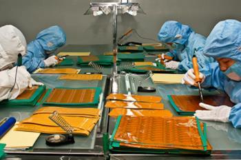
2 Manufacturing Infrastructure Manufacturing Infrastructure Scaling or just another FO Packaging Technology? 1) Panel Fan-Out Manufacturing is here for some time already for Embedded and Non-Embedded Packaging Technologies, Chip-First and Chip-Last - PCB (AT&S/ECP, Imbera/IMB, Schweizer Electronic/i²Board, ASE/aEASI, Many different ) formats; Lack of standardization; - LCD (PTI/PFO, SPLI/PFO, Samsung/PFO, Nepes/nPLP, ) Design Feature Limits; - Build-up OSAT (J-Devices/WFOP, TDK/SESUB, RDL-First, ASE/FOCLP, ) Yield constraints. 2) The hot topic is: Scaling of successful FOWLP Technologies to larger manufacturing formats; FOWLP = Embedded Packaging Technology (EPT) EMBEDDING has Chip-First inherent in the technology; - Semiconductor (IFX/eWLB, NANIUM/WLFO, JCET/eWLB, Nepes/RCP, ) Interconnect Technology is Thin-Film RDL (no WB, no FC); - Solar Semiconductor (DECA/M-Series, ) Substrate is Moldcompound, or Inorganic Materials (Si or Glass); - Silicon Foundry (TSMC/InFO,...) Interconnect btw die pad and package I/O is formed on die + substrate. Customer demand: - Same results (1:1 copy) at lower cost enabled by larger format; - No additional FO technology, but transfer of construction & BOM.

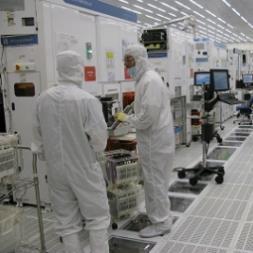

3 Wafer- and Panel-Level Manufacturing Environment IC-Substrate / PCB Manufacturing Environment Classical OSAT w/ Packaging & Test Backend - Environment WLP OSAT w/ Semiconductor Frontend - Environment
4 Package Size [mm²] Number of Dies/ Passives [#] The FOWLP Scaling Dilemma / WLFO Platform Approach Not to Scale! One BOM & POR fits all - Reliability Requirements - Manufacturability in HVM - FI & FO are Complementing - PKG vs MFG Format size Large Package vs Round Recon Wafer 80 Panel?! Current WLFO Sweet Spot 0 0 4mm x 4mm = 16mm² Wafer?! Silicon Occupation Ratio [%] 100 0
5 Scaling or just another FO Packaging Technology? - Manufacturing Format Scaling is a pure cost saving topic w/o impact on: - Package Construction; - Design Features; - Bill of Material (BOM); - Reliability and Quality; - Test results and Yield levels. FOWLP over FOPLP for project start phase for fast samples for small and medium volumes for complex WLSiP, WL3D products - Changes to Package Construction and BOM result in modified Packaging Technology and cannot be considered as Manufacturing Format Scaling - Economic Aspects have to be factored into the equation: - FOPLP has to be affordable for the industry (investment, volume, 2nd source, complexity, yield) - Deliver components to customer. Components packaged in fully loaded high yielding FOWLP line can be cheaper than components packaged in half-loaded low yielding FOPLP line!!!
6 The FOWLP Scaling Dilemmas / What is it about? Dilemma 1: FOWLP manufacturing format scaling to FOPLP has technical challenges; If solved by change in technology Another additional Shade of Fan-Out. Dilemma 2: Volumes for FOWLP are coming from high density and Package Stacking solutions e.g. TSMC`s InFO PoP Requires Semiconductor Environment = Wafer-Level. Dilemma 3: FOPLP manufacturing to utilize PCB, LCD or Build-up OSAT material, equipment, processes Cannot achieve the FOWLP design features and yield levels. Dilemma 4: FOWLP is increasingly used for more complex package constructions like WLSiP and WL3D with Passives and MEMS Complexity, high product mix, low volumes. Sweet Spot for FOPLP will be in large package sizes, but with low complexity (Single Die, 1L-RDL) and needs stable large volumes to continuously load the line.
System-in-Package (SiP) on Wafer Level, Enabled by Fan-Out WLP (ewlb)
 on Wafer Level, Enabled by Fan-Out WLP (ewlb)") System-in-Package (SiP) on Wafer Level, Enabled by Fan-Out WLP (ewlb) Steffen Kröhnert, José Campos, Eoin O Toole NANIUM S.A., Vila do Conde, Portugal Outline Short Company Overview NANIUM Introduction
System-in-Package (SiP) on Wafer Level, Enabled by Fan-Out WLP (ewlb) Steffen Kröhnert, José Campos, Eoin O Toole NANIUM S.A., Vila do Conde, Portugal Outline Short Company Overview NANIUM Introduction
Nanium Overview. Company Presentation
 Nanium Overview Company Presentation Nanium Overview Our name and logo nano prefix of Greek origin referring to small objects ium suffix of Latin origin that includes the formation of scientific terms
Fan-Out Packaging Technologies and Markets Jérôme Azémar
 Fan-Out Packaging Technologies and Markets Jérôme Azémar Senior Market and Technology Analyst at Yole Développement Outline Advanced Packaging Platforms & Market drivers Fan-Out Packaging Principle & Definition
TechARENA Packaging Exhibitor Session OCT/08, 2014 New WLP-Technology-Fusion Concept Steffen Kröhnert, Director of Technology, NANIUM S.A. V1.
 TechARENA Packaging Exhibitor Session OCT/08, 2014 New WLP-Technology-Fusion Concept Steffen Kröhnert, Director of Technology, NANIUM S.A. V1.0 EXT Notification NANIUM is highly committed to IP protection.
Panel Discussion: Advanced Packaging
 Dr. Steve Bezuk Senior Director IC Packaging Engineering Qualcomm Technologies, Inc. Panel Discussion: Advanced Packaging PAGE 1 Technical Challenges of Packaging (Mobile Focus) Materials Die materials
Development of Novel High Density System Integration Solutions in FOWLP Complex and Thin Wafer-Level SiP and Wafer-Level 3D Packages
 2017 IEEE 67th Electronic Components and Technology Conference Development of Novel High Density System Integration Solutions in FOWLP Complex and Thin Wafer-Level SiP and Wafer-Level 3D Packages André
Innovative Substrate Technologies in the Era of IoTs
 Innovative Substrate Technologies in the Era of IoTs Dyi- Chung Hu 胡迪群 September 4, 2015 Unimicron Contents Introduction Substrate Technology - Evolution Substrate Technology - Revolution Glass substrate
IME Technical Proposal. High Density FOWLP for Mobile Applications. 22 April High Density FOWLP Consortium Forum
 IME Technical Proposal High Density FOWLP for Mobile Applications 22 April 2014 Packaging driver for portable / mobile applications Key drivers/needs Smaller form-factor lower profile, substrate-less Higher
Graser User Conference Only
 2.5D/3D Design Solution Eric Chen & Scott Liu 31/Oct/2014 Roadmap data is provided for informational purposes only and does not represent a commitment to deliver any of the features or functionality discussed
Narrowing the Gap between Packaging and System
 Narrowing the Gap between Packaging and System Meptec Symposium 2015 ASE (US) Inc Ou Li Nov 10 th, 2015 Outline Industry Dynamics The Need for System Integrators IC/Pkg/System Collaboration Summary 2 Market
3D Package Technologies Review with Gap Analysis for Mobile Application Requirements. Apr 22, 2014 STATS ChipPAC Japan
 3D Package Technologies Review with Gap Analysis for Mobile Application Requirements Apr 22, 2014 STATS ChipPAC Japan T.Nishio Contents Package trends and roadmap update Advanced technology update Fine
Challenges and Solutions for Cost Effective Next Generation Advanced Packaging. H.P. Wirtz, Ph.D. MiNaPAD Conference, Grenoble April 2012
 Challenges and Solutions for Cost Effective Next Generation Advanced Packaging H.P. Wirtz, Ph.D. MiNaPAD Conference, Grenoble April 2012 Outline Next Generation Package Requirements ewlb (Fan-Out Wafer
Chip Packaging for Wearables Choosing the Lowest Cost Package
 Chip Packaging for Wearables Choosing the Lowest Cost Package Alan Palesko alanp@savansys.com (512) 402-9943 www.savansys.com Slide - 1 Agenda Introduction Wearable Requirements Packaging Technologies
Innovative Advanced Wafer Level Packaging with Smart Manufacturing Solutions YOON Seung Wook, Ph.D MBA
 Innovative Advanced Wafer Level Packaging with Smart Manufacturing Solutions YOON Seung Wook, Ph.D MBA Director, STATS ChipPAC Outline 1 2 3 Introduction of Smart Manufacturing & Wafer Level Packaging
SLIM TM, High Density Wafer Level Fan-out Package Development with Submicron RDL
 2017 IEEE 67th Electronic Components and Technology Conference SLIM TM, High Density Wafer Level Fan-out Package Development with Submicron RDL YoungRae Kim 1, JaeHun Bae 1, MinHwa Chang 1, AhRa Jo 1,
Development and Characterization of 300mm Large Panel ewlb (embedded Wafer Level BGA)
") Development and Characterization of 300mm Large Panel ewlb (embedded Wafer Level BGA) Seung Wook Yoon, Yaojian Lin and Pandi C. Marimuthu STATS ChipPAC Ltd. 5 Yishun Street 23, Singapore 768442 E-mail
Development and Characterization of 300mm Large Panel ewlb (embedded Wafer Level BGA) Seung Wook Yoon, Yaojian Lin and Pandi C. Marimuthu STATS ChipPAC Ltd. 5 Yishun Street 23, Singapore 768442 E-mail
Challenges of Fan-Out WLP and Solution Alternatives John Almiranez
 Challenges of Fan-Out WLP and Solution Alternatives John Almiranez Advanced Packaging Business Development Asia Introduction to Fan-Out WLP Introduction World of mobile gadgetry continues to rapidly evolve
IME Proprietary. EPRC 12 Project Proposal. 3D Embedded WLP. 15 th August 2012
 EPRC 12 Project Proposal 3D Embedded WLP 15 th August 2012 Motivation Factors driving IC market Higher density, lower cost, high yield Fan-out WLP/eWLP advantages Small footprint, low profile Low cost,
ewlb (embedded Wafer Level BGA) Technology: Next Generation 3D Packaging Solutions
 Technology: Next Generation 3D Packaging Solutions") ewlb (embedded Wafer Level BGA) Technology: Next Generation 3D Packaging Solutions by Seung Wook Yoon and Meenakshi Padmanathan STATS ChipPAC Ltd. Seungwook.yoon@statschippac.com Andreas Bahr Infineon
ewlb (embedded Wafer Level BGA) Technology: Next Generation 3D Packaging Solutions by Seung Wook Yoon and Meenakshi Padmanathan STATS ChipPAC Ltd. Seungwook.yoon@statschippac.com Andreas Bahr Infineon
First Demonstration of Panel Glass Fan-out (GFO) Packages for High I/O Density and High Frequency Multi-Chip Integration
 Packages for High I/O Density and High Frequency Multi-Chip Integration") 2017 IEEE 67th Electronic Components and Technology Conference First Demonstration of Panel Glass Fan-out (GFO) Packages for High I/O Density and High Frequency Multi-Chip Integration Tailong Shi, Chintan
2017 IEEE 67th Electronic Components and Technology Conference First Demonstration of Panel Glass Fan-out (GFO) Packages for High I/O Density and High Frequency Multi-Chip Integration Tailong Shi, Chintan
Between 2D and 3D: WLFO Packaging Technologies and Applications
 Between 2D and 3D: WLFO Packaging Technologies and Applications Minghao Shen Altera (now part of Intel) June 9 th, 2016 TFUG/CMPUG 3D Packaging Meeting Outline The 2.n D WLFO technologies Process and architect
Fan-out Wafer Level ewlb Technology as an Advanced System-in- Package Solution
 Fan-out Wafer Level ewlb Technology as an Advanced System-in- Package Solution by Jacinta Aman Lim and Vinayak Pandey, STATS ChipPAC, Inc. Aung Kyaw Oo, Andy Yong, STATS ChipPAC Pte. Ltd. Originally published
Wire-Bond CABGA A New Near Die Size Packaging Innovation Yeonho Choi February 1, 2017
 Amkor Technology, Inc. White Paper Wire-Bond CABGA A New Near Die Size Packaging Innovation Yeonho Choi February 1, 2017 Abstract Expanding its ChipArray Ball Grid Array (CABGA) package form factor miniaturization
Outline. Market Size Industry Trends Material Segment Trends China Summary. Packaging Materials Market Trends, Issues and Opportunities
 Packaging Materials Market Trends, Issues and Opportunities Dan Tracy Sr. Director Industry Research SEMI 8 th December 2015 Outline Market Size Industry Trends Material Segment Trends China Summary 1
A Cost Analysis of RDL-first and Mold-first Fan-out Wafer Level Packaging
 A Cost Analysis of RDL-first and Mold-first Fan-out Wafer Level Packaging Amy Palesko Lujan 1 1 SavanSys Solutions LLC, Austin, TX 78738, USA Abstract Industry interest in fan-out wafer level packaging
"ewlb Technology: Advanced Semiconductor Packaging Solutions"
 "ewlb Technology: Advanced Semiconductor Packaging Solutions" by Sharma Gaurav@, S.W. Yoon, Yap Yok Mian, Shanmugam Karthik, Yaojian Lin, Pandi C. Marimuthu and Yeong J. Lee* STATS ChipPAC Ltd. 5 Yishun
Close supply chain collaboration enables easy implementation of chip embedded power SiP
 Close supply chain collaboration enables easy implementation of chip embedded power SiP Gerald Weidinger, R&D Project Leader, AT&S AT & S Austria Technologie & Systemtechnik Aktiengesellschaft Fabriksgasse13
AN ANALYSIS OF KEY COST AND YIELD DRIVERS FOR FAN-OUT WAFER LEVEL PACKAGING
 AN ANALYSIS OF KEY COST AND YIELD DRIVERS FOR FAN-OUT WAFER LEVEL PACKAGING Amy Palesko SavanSys Solutions LLC Austin, TX, USA amyp@savansys.com ABSTRACT Although interest in wafer level packaging has
Cost effective 300mm Large Scale ewlb (embedded Wafer Level BGA) Technology
 Technology") Cost effective 300mm Large Scale ewlb (embedded Wafer Level BGA) Technology by Meenakshi Prashant, Seung Wook Yoon, Yaojian LIN and Pandi C. Marimuthu STATS ChipPAC Ltd. 5 Yishun Street 23, Singapore 768442
Cost effective 300mm Large Scale ewlb (embedded Wafer Level BGA) Technology by Meenakshi Prashant, Seung Wook Yoon, Yaojian LIN and Pandi C. Marimuthu STATS ChipPAC Ltd. 5 Yishun Street 23, Singapore 768442
Roundtable 3DIC & TSV: Ready for HVM? European 3D TSV Summit
 Roundtable 3DIC & TSV: Ready for HVM? European 3D TSV Summit Infineon VTI Xilinx Synopsys Micron CEA LETI 2013 Yann Guillou Business Development Manager Lionel Cadix Market & Technology Analyst, Advanced
Chips Face-up Panelization Approach For Fan-out Packaging
 Chips Face-up Panelization Approach For Fan-out Packaging Oct. 15, 2015 B. Rogers, D. Sanchez, C. Bishop, C. Sandstrom, C. Scanlan, TOlson T. REV A Background on FOWLP Fan-Out Wafer Level Packaging o Chips
RF System in Packages using Integrated Passive Devices
 RF System in Packages using Integrated Passive Devices by Kai Liu, YongTaek Lee, HyunTai Kim, Gwang Kim, and Billy Ahn STATS ChipPAC 1711 W. Greentree Drive, Suite #117, Tempe, AZ 85284, USA Tel: 480-222-1722
Fraunhofer IZM. All Silicon System Integration Dresden Scope. M. Juergen Wolf
 Fraunhofer IZM All Silicon System Integration Dresden Scope M. Juergen Wolf Fraunhofer IZM All Silicon System Integration - ASSID Dresden, Berlin, Germany Fraunhofer IZM Focus of Activities Materials,
Thales vision & needs in advanced packaging for high end applications
 Thales vision & needs in advanced packaging for high end applications M. Brizoux, A. Lecavelier Thales Global Services / Group Industry Chemnitzer Seminar June 23 th -24 th, 2015 Fraunhofer ENAS - Packaging
Next Gen Packaging & Integration Panel
 Next Gen Packaging & Integration Panel ECTC 2012 Daniel Tracy, Sr. Director Industry Research & Statistics SEMI May 29, 2012 Packaging Supply Chain Market Trends Material Needs and Opportunities Market
Innovative Integration Solutions for SiP Packages Using Fan-Out Wafer Level ewlb Technology
 Innovative Integration Solutions for SiP Packages Using Fan-Out Wafer Level ewlb Technology Jacinta Aman Lim, Vinayak Pandey* STATS ChipPAC Inc. 46429 Landing Parkway, Fremont, CA 94538, USA *STATS ChipPAC
A Flexible Vertical MEMs Probe Card Technology for Pre-Bump and ewlp Applications
 June 12 to 15, 2011 San Diego, CA A Flexible Vertical MEMs Probe Card Technology for Pre-Bump and ewlp Applications Mike Slessor Rick Marshall (MicroProbe, Inc.) Vertical MEMS for Pre-Bump Probe Introduction:
IMPLEMENTATION OF A FULLY MOLDED FAN-OUT PACKAGING TECHNOLOGY
 IMPLEMENTATION OF A FULLY MOLDED FAN-OUT PACKAGING TECHNOLOGY B. Rogers, C. Scanlan, and T. Olson Deca Technologies, Inc. Tempe, AZ USA boyd.rogers@decatechnologies.com ABSTRACT Fan-Out Wafer-Level Packaging
Equipment and Process Challenges for the Advanced Packaging Landscape
 Equipment and Process Challenges for the Advanced Packaging Landscape Veeco Precision Surface Processing Laura Mauer June 2018 1 Copyright 2018 Veeco Instruments Inc. Outline» Advanced Packaging Market
Towards Industrialization of Fan-out Panel Level Packaging
 Towards Industrialization of Fan-out Panel Level Packaging Tanja Braun S. Voges, O. Hölck, R. Kahle, S. Raatz, K.-F. Becker, M. Wöhrmann, L. Böttcher, M. Töpper, R. Aschenbrenner 1 Outline Introduction
Development of Next-Generation ewlb Packaging
 Development of Next-Generation ewlb Packaging by Seung Wook Yoon, Yaojian Lin, Pandi Chelvam Marimuthu and *Rajendra Pendse STATS ChipPAC Singapore *Fremont, California USA Ganesh V. P, Andreas Bahr and
Challenges for Embedded Device Technologies for Package Level Integration
 Challenges for Embedded Device Technologies for Package Level Integration Kevin Cannon, Steve Riches Tribus-D Ltd Guangbin Dou, Andrew Holmes Imperial College London Embedded Die Technology IMAPS-UK/NMI
Advanced 3D ewlb PoP (embedded Wafer Level Ball Grid Array Package on Package) Technology
 Technology") Advanced 3D ewlb PoP (embedded Wafer Level Ball Grid Array Package on Package) Technology by Kang Chen, Jose Alvin Caparas, Linda Chua, Yaojian Lin and *Seung Wook Yoon STATS ChipPAC Ltd. 5 Yishun Street
Advanced 3D ewlb PoP (embedded Wafer Level Ball Grid Array Package on Package) Technology by Kang Chen, Jose Alvin Caparas, Linda Chua, Yaojian Lin and *Seung Wook Yoon STATS ChipPAC Ltd. 5 Yishun Street
3D Integrated ewlb /FO-WLP Technology for PoP & SiP
 3D Integrated ewlb /FO-WLP Technology for PoP & SiP by Yaojian Lin, Chen Kang, Linda Chua, Won Kyung Choi and *Seung Wook Yoon STATS ChipPAC Pte Ltd. 5 Yishun Street 23, Singapore 768442 *STATS ChipPAC
Building an EcoSystem for User-friendly Design of Advanced System in Package (SiP) Solutions
 Solutions") Building an EcoSystem for User-friendly Design of Advanced System in Package (SiP) Solutions Herb Reiter eda 2 asic Consulting, Inc. IMAPS, Oct 9 12 & MEPTEC, Nov 13, 2017 Herb@eda2asic.com IMAPS 50 th
Building an EcoSystem for User-friendly Design of Advanced System in Package (SiP) Solutions Herb Reiter eda 2 asic Consulting, Inc. IMAPS, Oct 9 12 & MEPTEC, Nov 13, 2017 Herb@eda2asic.com IMAPS 50 th
Copyright 2009 Year IEEE. Reprinted from 2009 Electronic Components and Technology Conference. Such permission of the IEEE does not in any way imply
 Copyright 2009 Year IEEE. Reprinted from 2009 Electronic Components and Technology Conference. Such permission of the IEEE does not in any way imply IEEE endorsement of any of Institute of Microelectronics
Next Generation ewlb (embedded Wafer Level BGA) Packaging
 Packaging") Next Generation ewlb (embedded Wafer Level BGA) Packaging by Meenakshi Prashant, Kai Liu, Seung Wook Yoon Yonggang Jin, Xavier Baraton, S. W. Yoon*, Yaojian Lin*, Pandi C. Marimuthu*, V. P. Ganesh**, Thorsten
Next Generation ewlb (embedded Wafer Level BGA) Packaging by Meenakshi Prashant, Kai Liu, Seung Wook Yoon Yonggang Jin, Xavier Baraton, S. W. Yoon*, Yaojian Lin*, Pandi C. Marimuthu*, V. P. Ganesh**, Thorsten
HIGH PRODUCTIVITY UBM/RDL DEPOSITION BY PVD FOR FOWLP APPLICATIONS
 HIGH PRODUCTIVITY UBM/RDL DEPOSITION BY PVD FOR FOWLP APPLICATIONS Chris Jones, David Butler, Steve Burgess, Tony Wilby, Paul Densley SPTS Technologies Ltd Newport, United Kingdom chris.jones@orbotech.com
Forschung für die Elektroniksysteme von morgen
 Forschung für die Elektroniksysteme von morgen R. Aschenbrenner Outline Trends in Advanced Packaging Was ist Panel Level Packaging Embedding für Fan Out Embedding für LP Beispiele Trend on ICs and Packages
Thermal Management in Today's Electronic Systems
 Thermal Management in Today's Electronic Systems Darvin Edwards TI Fellow Manager, Advanced Package Modeling and Characterization Texas Instruments 1 COST SIZE POWER Packaging Technology Trends P-DIP PLCC
Board Level Reliability Improvement in ewlb (Embedded Wafer Level BGA) Packages
 Packages") Board Level Reliability Improvement in ewlb (Embedded Wafer Level BGA) Packages by Seng Guan Chow, Yaojian Lin, Bernard Adams * and Seung Wook Yoon** STATS ChipPAC Ltd. 5 Yishun Street 23, Singapore 768442
Board Level Reliability Improvement in ewlb (Embedded Wafer Level BGA) Packages by Seng Guan Chow, Yaojian Lin, Bernard Adams * and Seung Wook Yoon** STATS ChipPAC Ltd. 5 Yishun Street 23, Singapore 768442
Fanout Flipchip ewlb (embedded Wafer Level Ball Grid Array) Technology as 2.5D Packaging Solution
 Technology as 2.5D Packaging Solution") Fanout Flipchip ewlb (embedded Wafer Level Ball Grid Array) Technology as 2.5D Packaging Solution by Seung Wook Yoon,*Patrick Tang, **Roger Emigh, Yaojian Lin, Pandi C. Marimuthu, and *Raj Pendse STATS
Fanout Flipchip ewlb (embedded Wafer Level Ball Grid Array) Technology as 2.5D Packaging Solution by Seung Wook Yoon,*Patrick Tang, **Roger Emigh, Yaojian Lin, Pandi C. Marimuthu, and *Raj Pendse STATS
IMPLEMENTING FAN-OUT WAFER-LEVEL PACKAGING (FOWLP) WITH THE MENTOR HDAP FLOW JOHN FERGUSON AND KEITH FELTON, MENTOR, A SIEMENS BUSINESS
 WITH THE MENTOR HDAP FLOW JOHN FERGUSON AND KEITH FELTON, MENTOR, A SIEMENS BUSINESS") IMPLEMENTING FAN-OUT WAFER-LEVEL PACKAGING (FOWLP) WITH THE MENTOR HDAP FLOW JOHN FERGUSON AND KEITH FELTON, MENTOR, A SIEMENS BUSINESS D E S I G N T O S I L I C O N W H I T E P A P E R w w w. m e n t
IMPLEMENTING FAN-OUT WAFER-LEVEL PACKAGING (FOWLP) WITH THE MENTOR HDAP FLOW JOHN FERGUSON AND KEITH FELTON, MENTOR, A SIEMENS BUSINESS D E S I G N T O S I L I C O N W H I T E P A P E R w w w. m e n t
Electrical and Fluidic Microbumps and Interconnects for 3D-IC and Silicon Interposer
 Electrical and Fluidic Microbumps and Interconnects for 3D-IC and Silicon Interposer Li Zheng, Student Member, IEEE, and Muhannad S. Bakir, Senior Member, IEEE Georgia Institute of Technology Atlanta,
Warpage Tuning Study for Multi-chip Last Fan Out Wafer Level Package
 2017 IEEE 67th Electronic Components and Technology Conference Warpage Tuning Study for Multi-chip Last Fan Out Wafer Level Package Hung-Yuan Li, Allen Chen, Sam Peng, George Pan, and Stephen Chen Siliconware
Compression molding encapsulants for wafer-level embedded active devices
 2017 IEEE 67th Electronic Components and Technology Conference Compression molding encapsulants for wafer-level embedded active devices Wafer warpage control by epoxy molding compounds Kihyeok Kwon, Yoonman
Thin Wafers Bonding & Processing
 Thin Wafers Bonding & Processing A market perspective 2012 Why New Handling Technologies Consumer electronics is today a big driver for smaller, higher performing & lower cost device configurations. These
Package Solutions and Innovations
 Package Solutions and Innovations with Compression Molding IEEE SVC CPMT Aug 2015 Presented by C.H. Ang Towa USA Company Profile www.cpmt.org/scv 1 Corporate Overview Company: Towa Corp., Kyoto Japan Established:
SEMI MEMS Tech Seminar (Sept 26, Cornaredo, Italy)
") SEMI MEMS Tech Seminar (Sept 26, 2013 - Cornaredo, Italy) Opportunities of Wafer Level Embedded Technologies for MEMS Devices T. Braun ( 1 ), K.-F. Becker ( 1 ), R. Kahle ( 2 ), V. Bader ( 1 ), S. Voges
SEMI MEMS Tech Seminar (Sept 26, 2013 - Cornaredo, Italy) Opportunities of Wafer Level Embedded Technologies for MEMS Devices T. Braun ( 1 ), K.-F. Becker ( 1 ), R. Kahle ( 2 ), V. Bader ( 1 ), S. Voges
Design and Assembly Process Implementation of 3D Components
 IPC-7091 Design and Assembly Process Implementation of 3D Components Developed by the 3-D Electronic Packages Subcommittee (B-11) of the Packaged Electronic Components Committee (B-10) of IPC Users of
Cost Comparison of Fan-out Wafer-Level Packaging to Fan-out Panel- Based Packaging
 Cost Comparison of Fan-out Wafer-Level Packaging to Fan-out Panel- Based Packaging Chet Palesko, Amy Lujan SavanSys Solutions LLC 10409 Peonia Ct. Austin, TX 78733 Ph: 512-402-9943 chetp@savansys.com,
System Level Design and Simulation for Heterogeneous Integration
 System Level Design and Simulation for Heterogeneous Integration Presented by Bill Bottoms PhD bill_bottoms@3mts.com Electronic Design Process Symposium SEMI, Milpitas, California September 21 22, 2017
Test Flow for Advanced Packages (2.5D/SLIM/3D)
") 1 Test Flow for Advanced Packages (2.5D/SLIM/3D) Gerard John Amkor Technology Inc. Gerard.John@amkor.com 2045 East Innovation Circle, Tempe, AZ 85284, USA Phone: (480) 821-5000 ADVANCED PACKAGE TEST FLOW
1 Test Flow for Advanced Packages (2.5D/SLIM/3D) Gerard John Amkor Technology Inc. Gerard.John@amkor.com 2045 East Innovation Circle, Tempe, AZ 85284, USA Phone: (480) 821-5000 ADVANCED PACKAGE TEST FLOW
Hot Chips: Stacking Tutorial
 Hot Chips: Stacking Tutorial Choon Lee Technology HQ, Amkor Enabling a Microelectronic World Mobile Phone Technology Change Feature Phone Smartphone Smartphones as a Percentage of All Phones Source : The
Glass Carrier for Fan Out Panel Level Package
 January 25, 2018 NEWS RELEASE Development of HRDP TM Material for Formation of Ultra-Fine Circuits with Glass Carrier for Fan Out Panel Level Package - Aiming for mass production in collaboration with
Increasing challenges for size and cost reduction,
 Packageon-Package: The Story Behind This Industry Hit Package-onpackage (PoP) technology is rapidly evolving to keep pace with the demand for faster, higherdensity devices in smaller, thinner stacks. As
Material based challenge and study of 2.1, 2.5 and 3D integration
 1 Material based challenge and study of 2.1, 2.5 and 3D integration Toshihisa Nonaka Packaging Solution Center R&D Headquarters Hitachi Chemical Co., Ltd., Sep. 8, 2016 Hitachi Chemical Co., Ltd. 2010.
Semiconductor IC Packaging Technology Challenges: The Next Five Years
 SPAY025 May 2006 White Paper Mario A. Bolanos, Director Semiconductor Group Packaging Technology Development, Texas Instruments In the era of communications and entertainment, growth of consumer electronics
Novel Materials and Activities for Next Generation Package. Hitachi Chemical., Co.Ltd. Packaging Solution Center Hiroaki Miyajima
 Novel Materials and Activities for Next Generation Package Hitachi Chemical., Co.Ltd. Packaging Solution Center Hiroaki Miyajima 1. Activities of Packaging Solution Center 2. Novel Materials for Next Gen.
Lehman Brothers Global Technology Conference. December 2007
 Lehman Brothers Global Technology Conference December 2007 Oleg Khaykin Joanne Solomon EVP & COO Chief Financial Officer Forward Looking Statement Disclaimer All information and other statements contained
Rudolph Technologies. Investor Presentation. Sidoti Conference, September 2018
 Rudolph Technologies Investor Presentation Sidoti Conference, September 2018 Building a Business for Sustainable Growth Increasing the pace of innovation while driving operational efficiencies Company
Credit Suisse Technology Conference
 Credit Suisse Technology Conference November 2007 Oleg Khaykin Ken Joyce Jim Fusaro EVP & COO Chief Administrative Officer Corporate VP, Wire Bond Products Forward Looking Statement Disclaimer All information
Enabling Technology in Thin Wafer Dicing
 Enabling Technology in Thin Wafer Dicing Jeroen van Borkulo, Rogier Evertsen, Rene Hendriks, ALSI, platinawerf 2G, 6641TL Beuningen Netherlands Abstract Driven by IC packaging and performance requirements,
The Role of Wafer Foundries in Next Generation Packaging. David McCann, VP Packaging R+D May 28, 2013
 The Role of Wafer Foundries in Next Generation Packaging David McCann, VP Packaging R+D May 28, 2013 Page 1 Solutions are Increasingly Silicon-Based RF moves from QFN to wlcsp Driven by footprint and cost
Qualcomm WCD9335 Fan-Out WLP Audio Codec
 Qualcomm WCD9335 Fan-Out WLP Audio Codec Qualcomm s Fan-Out Wafer-Level Package Chip Audio Codec in ewlb Package inside Samsung Galaxy S7 and S7 Edge Qualcomm, a world leader in mobile technologies, offers
NXP SCM-i.MX6 Quad High Density Fan-Out Wafer-Level System-in-Package
 NXP SCM-i.MX6 Quad High Density Fan-Out Wafer-Level System-in-Package The first ultra-small multi-die low power module with boot memory and power management integrated in a package-on-package compatible
Effects of Design, Structure and Material on Thermal-Mechanical Reliability of Large Array Wafer Level Packages
 Effects of Design, Structure and Material on Thermal-Mechanical Reliability of Large Array Wafer Level Packages Bhavesh Varia 1, Xuejun Fan 1, 2, Qiang Han 2 1 Department of Mechanical Engineering Lamar
System in Package: Identified Technology Needs from the 2004 inemi Roadmap
 System in Package: Identified Technology Needs from the 2004 inemi Roadmap James Mark Bird Amkor Technology Inc System in package (SiP) technology has grown significantly in the past several years. It
3D technologies for More Efficient Product Development
 3D technologies for More Efficient Product Development H. Ribot, D. Bloch, S. Cheramy, Y. Lamy, P. Leduc, T. Signamarcheix, G. Simon Semicon Europa, TechArena II, 09 October 2013 Photonics in Product development:
Technical Viability of Stacked Silicon Interconnect Technology
 Technical Viability of Stacked Silicon Interconnect Technology Dr. Handel H. Jones Founder and CEO, IBS Inc. Los Gatos, California October 2010 TECHNICAL VIABILITY OF STACKED SILICON INTERCONNECT TECHNOLOGY
Development of Super Thin TSV PoP
 Development of Super Thin TSV PoP by Seung Wook Yoon, *Kazuo Ishibashi, Shariff Dzafir, Meenakshi Prashant, Pandi Chelvam Marimuthu and **Flynn Carson STATS ChipPAC Ltd. 5 Yishu n Street 23, Singapore
Factors Influencing Semiconductor Package Migration
 Factors Influencing Semiconductor Package Migration by Tom Strothmann and Kevin Kan Tempe, AZ, USA STATS ChipPAC, Inc Originally published in the International Wafer Level Packaging Conference Proceedings,
Heat Dissipation Capability of a Package-on- Package Embedded Wafer-Level Package
 1 Heat Dissipation Capability of a Package-on- Package Embedded Wafer-Level Package Yong Han, Boon Long Lau, Boo Yang Jung, Xiaowu Zhang, Senior Member, IEEE Abstract As the embedded wafer-level packaging
Silicon Interposer with Embedded Microfluidic Cooling for High-Performance Computing Systems
 Silicon Interposer with Embedded Microfluidic Cooling for High-Performance Computing Systems Li Zheng 1, Yang Zhang, Xuchen Zhang and Muhannad S. Bakir 2 School of Electrical and Computer Engineering Georgia
Failure Analysis for ewlb-packages Strategy and Failure Mechanisms
 Company Logo Failure Analysis for ewlb-packages Strategy and Failure Mechanisms Florian Felux Infineon Technologies AG Neubiberg, Germany Purpose Demonstration of adaption and application of various analysis
Atul Gupta, Eric Snyder, Christiane Gottschalk, Kevin Wenzel, James Gunn
 First Demonstration of Photoresist Cleaning for Fine-Line RDL Yield Enhancement by an Innovative Ozone Treatment Process for Panel Fan-out and Interposers Atul Gupta, Eric Snyder, Christiane Gottschalk,
3D-WLCSP Package Technology: Processing and Reliability Characterization
 3D-WLCSP Package Technology: Processing and Reliability Characterization, Paul N. Houston, Brian Lewis, Fei Xie, Ph.D., Zhaozhi Li, Ph.D.* ENGENT Inc. * Auburn University ENGENT, Inc. 2012 1 Outline Packaging
Engineered Substrates
 Engineered Substrates Engineered Substrates Using the NanoCleave TM Process Francois J. Henley President and CEO Silicon Genesis Corporation San Jose, California SiGen Presentation Outline Engineered Substrates
Chapter 4 Fabrication Process of Silicon Carrier and. Gold-Gold Thermocompression Bonding
 Chapter 4 Fabrication Process of Silicon Carrier and Gold-Gold Thermocompression Bonding 4.1 Introduction As mentioned in chapter 2, the MEMs carrier is designed to integrate the micro-machined inductor
Two Chips Vertical Direction Embedded Miniaturized Package
 Two Chips Vertical Direction Embedded Miniaturized Package Shunsuke Sato, 1 Koji Munakata, 1 Masakazu Sato, 1 Atsushi Itabashi, 1 and Masatoshi Inaba 1 Continuous efforts have been made to achieve seemingly
Advanced Packaging. End-to-end solution chains for WLSiP
 Advanced Packaging End-to-end solution chains for WLSiP Advanced Packaging/WLSiP 3 The whole solution chain from a single source 4 E-forming produces the finest multi-level apertures 6 The printing solution
Bonding Technologies for 3D-Packaging
 Dresden University of Technology / Karsten Meier, Klaus-Juergen Wolter NanoZEIT seminar @ SEMICON Europa 2011 Dresden System integration by SoC or SiP solutions offer advantages regarding design efforts,
Material Selection and Parameter Optimization for Reliable TMV Pop Assembly
 Selection and Parameter Optimization for Reliable TMV Pop Assembly Brian Roggeman, David Vicari Universal Instruments Corp. Binghamton, NY, USA Roggeman@uic.com Martin Anselm, Ph.D. - S09_02.doc Lee Smith,
Recent Advances in Die Attach Film
 Recent Advances in Die Attach Film Frederick Lo, Maurice Leblon, Richard Amigh, and Kevin Chung. AI Technology, Inc. 70 Washington Road, Princeton Junction, NJ 08550 www.aitechnology.com Abstract: The
System-in-Package Research within the IeMRC
 LANCASTER U N I V E R S I T Y Centre for Microsystems Engineering Faculty of Applied Sciences System-in-Package Research within the IeMRC Prof. Andrew Richardson (Lancaster University) Prof. Chris Bailey
Kun Young Chung Design Technology Team System LSI Samsung Electronics
 2012 Test Technology Workshop (Oct. 31, 2012) IDC-System LSI Business 0 Kun Young Chung Design Technology Team System LSI Samsung Electronics An Overview: Test Challenges in 3D ICs Design (Design-for-Test)
ECE414/514 Electronics Packaging Spring 2012 Lecture 2. Lecture Objectives
 ECE414/514 Electronics Packaging Lecture 2 James E. Morris Dept of Electrical & Computer Engineering Portland State University Lecture Objectives Introduce first-level interconnect technologies: wire-bond,
Cu Pillar Interconnect and Chip-Package-Interaction (CPI) for Advanced Cu Low K chip
 for Advanced Cu Low K chip") EPRC 12 Project Proposal Cu Pillar Interconnect and Chip-Package-Interaction (CPI) for Advanced Cu Low K chip 15 th Aug 2012 Page 1 Introduction: Motivation / Challenge Silicon device with ultra low k
EPRC 12 Project Proposal Cu Pillar Interconnect and Chip-Package-Interaction (CPI) for Advanced Cu Low K chip 15 th Aug 2012 Page 1 Introduction: Motivation / Challenge Silicon device with ultra low k
Challenges for Power, Signal, and Reliability Verification on 3D-IC/Silicon Interposer Designs. Norman Chang, VP and Sr. Product Strategist
 Challenges for Power, Signal, and Reliability Verification on 3D-IC/Silicon Interposer Designs Norman Chang, VP and Sr. Product Strategist 1 2012 ANSYS, Inc. August 31, 2012 Outline 3D-IC/Silicon Interposer
Considerations for Embedding Passives and Actives in PCBs
 Considerations for Embedding Passives and Actives in PCBs PwrSoC 2014 AT & S Austria Technologie & Systemtechnik Aktiengesellschaft Fabriksgasse 13 A-8700 Leoben Tel +43 (0) 3842 200-0 E-mail info@ats.net