Electron Beam Induced Processes and their Applicability to Mask Repair
|
|
|
- Giles Boyd
- 6 years ago
- Views:
Transcription
 LEO Elektronenmikroskopie GmbH Oberkochen Germany greiser@leo.de, Tel: +49 7364 944757, Fax: +49 7364 944670 1 ISMT/Selete Antwerpen 8.9.2002")
1 & Electron Beam Induced Processes and their Applicability to Mask Repair Hans W.P. Koops (1), Volker Boegli (1), Klaus Edinger (1), Johannes Bihr (2), Jens Greiser (2), (1) NaWoTec GmbH Rossdorf Germany Tel: , Fax: (2) LEO Elektronenmikroskopie GmbH Oberkochen Germany Tel: , Fax: ISMT/Selete Antwerpen
2 Outline Principle of 3-D-Lithography Why e-beam mask repair 70nm mask repair tool strategy Specifications Experimental tool Performance capability Alpha-tool Capability Deposition results and AIMS characterization Key engineering / development challenges Extendibility and roadmap Conclusion 2 ISMT / SELETE Antwerpen &
3 Principle of 3-Dimensional Lithography using Electron-Beam Induced Deposition and Etching Organometallic precursor Nozzle Electron beam Residual gas Evaporating radicals Deposit Adsorbed molecules Sample Electron Beam induced reactions of adsorbed molecules by electrons of high energy Power density: 60 MW/cm 2 -> Deposition of fragments -> Evaporation of reaction products 3 ISMT / SELETE Antwerpen &


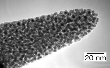
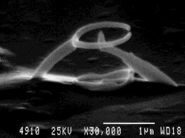
4 1 µm 4 ISMT / SELETE Antwerpen &

5 Why E-Beam Mask Repair? Ion beams generate unavoidable substrate damage by ion implantation and mixing No solution for chemical reactions below 80 nm is demonstrated Electron beams avoid substrate damage and allow high resolution Courtesy: Ted Liang: 157 nm Workshop Dana Point Only the LEO Gemini optics meets the high resolution specs 5 ISMT / SELETE Antwerpen &
![Operating Principle of the Objective Lens Magnetic lens Aberration Coefficients [mm] 25 20 15 Spherical 10 5 Chromatic 0 0 5 10 15 20 25 30 Beam Energy [KeV] Electrostatic lens Compound](/docs-images/76/73231998/images/6-0.jpg "magnetic/electrostatic objective lens has smaller aberrations than pure electrostatic or magnetic lens Usually the objective lens aberrations are constants.")
6 Operating Principle of the Objective Lens Magnetic lens Aberration Coefficients [mm] Spherical 10 5 Chromatic Beam Energy [KeV] Electrostatic lens Compound magnetic/electrostatic objective lens has smaller aberrations than pure electrostatic or magnetic lens Usually the objective lens aberrations are constants. Due to the GEMINI operation principle lens aberrations are coefficients which show a dramatic reduction at low beam energy 6 ISMT / SELETE Antwerpen &
7 Clean Mask Repair using E- Beam Chemistry Base Tool: LEO high performance GEMINI 1500 VP FE-SEM 100 V to 30 kv, 1pA to 20 na, Schottky field emitter column with low Cs and Cc, in-lens detector, 6 mask /8 wafer, interferometer controlled stage Gas supply system Multi-Jet: NaWoTec design and production, interfaced to the e-beam platform Deposition and etching: NaWoTec beam control system Active drift compensation Proprietory recipes Custom designed specialized solutions 7 ISMT / SELETE Antwerpen &
8 Co-operation: Photo Mask Repair Tool PMRT NaWoTec LEO FE-SEM 1500 VP Gas supply system Beam control Active drift compensation Image processing Defect compensation Repair process control Application laboratory Continued development Computer Interface to SEM VP-SEM V 30 kv Motorstage Laser interferometer Airlock Hot FE-gun 1 pa - 20 na Beam blanking Service of PMRT Marketing & Sales 8 ISMT / SELETE Antwerpen &

9 E-beam Mask Repair Experimental System Based on the LEO 1530 VP FE-SEM with NaWoTec s 4-Channel Multi-Jet software controlled gas supply system, pattern generator, control and GUI Installed at NaWoTec s Application Lab 9 ISMT / SELETE Antwerpen &

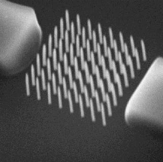
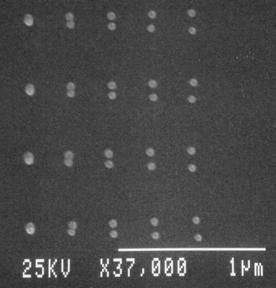
10 High Resolution Patterning with Deposition Platinum deposition with the experimental- PMRT on Cr demonstrates: 20 nm features < 4 nm edge roughness < 10 nm drift/min highly accurate pattern generation 10 ISMT / SELETE Antwerpen &
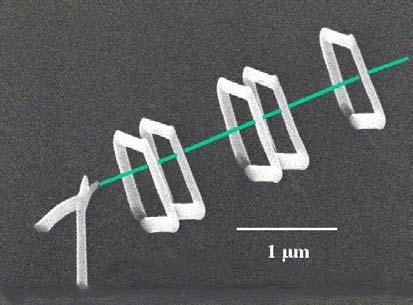
11 Deposition with 5 the kv,17 Experimental 5kV pa17pa System Pt/C deposition using LEO 1530 VP FSEM and NaWoTec Multi-Jet 1 kv 17 pa 500 V 13 Picture taken at 30 tilt Experimental Pt-supply: kv 500 nm x 500 nm, 80 nm thickness deposited in 30 sec 300 V 12 p 11 ISMT / SELETE Antwerpen &

12 E-beam Mask Repair Alpha-Tool LEO base system: 1500 VP FE-SEM GEMINI column VP vacuum system 8 wafer, 6 mask Airlock Laser interferometer NaWoTec integrates: 4-channel Multi-Jet software controlled gas supply system Pattern generator Control and GUI Defect cruising Repair procedures Drift compensation 12 ISMT / SELETE Antwerpen &

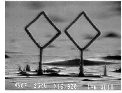
13 Deposition of Pt/C bars on quartz between chromium lines 1 µm Deposition time for 1 µm x 1 µm, 80 nm thick is 2 minutes, 248 nm shows good process control for 3 sets of structures NA = 0,54 Rel. Intensity X-Position [µm] 13 ISMT / SELETE Antwerpen & set1x.aim set2x.aim set3x.aim


14 Deposition of Pt/C bars on quartz nm of attennuation of structures of equal size, NA = 0,54 a15.aim ref.aim Pt/C-deposit and chrome Square, 1.2 kv, 50pA a15.aim ref.aim y 14 ISMT / SELETE Antwerpen &

15 Demonstration of TaN etching Etching of TaN is performed using XeF 2 at 1 kv, 17 pa Etch depth 70 nm Etch time for 1 µm x 1 µm 70 nm deep is 5 sec 15 ISMT / SELETE Antwerpen &

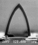
16 Demonstration of stencil mask repair with Pt/C- 3-D-deposition 100 nm Deposition of Pt/C bridges across Si-membrane gap 16 ISMT / SELETE Antwerpen &
17 E-beam Mask Repair Top 3 Challenges Chrome etching Compensation of charging effects Avoid contamination at low kv 17 ISMT / SELETE Antwerpen &
18 NaWoTec & LEO PMRT- Development Roadmap Year Quarter Q1 Q2 Q3 Q4 Q1 Q2 Q3 Q4 Exp. PMRT 1530/Multi-Jet α-tool PMRT (1500VP/Multi-Jet) β-tool (PMRT) β-tool: factory acceptance month after order 18 ISMT / SELETE Antwerpen &
19 Beta- and Production Tool Key Characteristics Beta tool 1500 VP based semi-automatic operation open defect repair closed defect repair 6 mask / 8 wafer chamber laser interferometer stage meets SEMI S2/S8 specs Production tool enhancements fully automatic open and closed defect repair 9 mask chamber (12 if req.) autoloader available Q4/2003 available Q4/2005 Systems can be upgraded with new deposition/etch recipes Tool meets the repair requirements of the 70 nm device node and is extendible to 50 nm and potentially 35 nm nodes 19 ISMT / SELETE Antwerpen &
20 Conclusion NaWoTec and LEO jointly develop an electron beam based Photo Mask Repair Tool Initial marketing and support jointly by NaWoTec and LEO Worldwide sales and services by LEO Application laboratory at NaWoTec Continued develompment by NaWoTec β- tool will meet the 70 nm node requirements So far demonstrated: High resolution Pt/C deposition High resolution etching of quartz, SiO 2, SiC and TaN 20 ISMT / SELETE Antwerpen &
21 Discussion foils 21 ISMT / SELETE Antwerpen &
22 Company Overview: NaWoTec GmbH Nano World Technologies Founded as a Spin-Off from T-Nova, Deutsche Telekom AG 25 full time employees, 11 temporary employees Technical advisors from international companies and universities Office and laboratory building sqft Clean room laboratory 1800 sqft class 1000 Clean room applications, assembly 1000 sqft class Experimental SEM s with Multi-Jet for deposition and etching 1 α-tool LEO 1500VP based, 8 Chamber, Multi-Jet 2 Experimental nanolithography systems 22 ISMT / SELETE Antwerpen &
23 NaWoTec Mission and Visions Development and production of a system for nanolithography with electron-beam induced reactions for photo- and NGL- mask repair for the semiconductor industry Development and production of novel and innovative components for : Bio-nano-technology Electronics Field emitter applications Medical applications Optics and telecommunications 23 ISMT / SELETE Antwerpen &
24 Carl Zeiss Semiconductor Manufacturing Technology AG CEO: Dr. D. Kurz Legal Structure since October 2001 Carl Zeiss Carl Zeiss S-M-T AG CEO: Dr. H. Gerlinger CFO: D. Schoch. Employees: 1600 LEO Group CEO: Dr. D. Stenkamp CFO: R. Yoder LEO GmbH (GER) Employees: 360 LEO Inc. (USA) LEO Ltd. (UK) LEO S.A. (F) 24 ISMT / SELETE Antwerpen &


25 Carl Zeiss S-M-T AG Product Portfolio for Key IC Manufacturing Lithography Mask Inspection & E-beam Repair CZ MES LEO Group Wafer Inspection, Review and Failure Analysis 25 ISMT / SELETE Antwerpen &


26 Total Solutions for Masks (CZ SMT AG) NaWoTec & LEO CZ MES GmbH E-beam Mask Repair Tool In co-operation with AIMS fab 26 ISMT / SELETE Antwerpen &
27 Electron Optics of the LEO 1500 VP Beam path with no intermediate cross over Electromagnetic aperture changer Field lens In-lens SE-detector Beam booster Magnetic lens Scan coils Electrostatic lens Specimen U Ex U L U 0 Highly stable thermal FEG <0.5%/h variation Low beam noise1% Cross over free beam path No significant Boersch effect, high depth of field. Low aberrations C c and C s Superb image resolution throughout the whole beam energy range, particularly down to 100eV. High resistance to ambient magnetic stray fields. 27 ISMT / SELETE Antwerpen &
28 Schematic of the Photo Mask repair Tool LEO GEMINI 28 ISMT / SELETE Antwerpen &
Nanoscale Imaging, Material Removal and Deposition for Fabrication of Cutting-edge Semiconductor Devices
 Hitachi Review Vol. 65 (2016), No. 7 233 Featured Articles Nanoscale Imaging, Material Removal and Deposition for Fabrication of Cutting-edge Semiconductor Devices Ion-beam-based Photomask Defect Repair
Micro- and Nano-Technology... for Optics
 Micro- and Nano-Technology...... for Optics 3.2 Lithography U.D. Zeitner Fraunhofer Institut für Angewandte Optik und Feinmechanik Jena Electron Beam Column electron gun beam on/of control magnetic deflection
Introduction to Lithography
 Introduction to Lithography G. D. Hutcheson, et al., Scientific American, 290, 76 (2004). Moore s Law Intel Co-Founder Gordon E. Moore Cramming More Components Onto Integrated Circuits Author: Gordon E.
EECS130 Integrated Circuit Devices
 EECS130 Integrated Circuit Devices Professor Ali Javey 9/13/2007 Fabrication Technology Lecture 1 Silicon Device Fabrication Technology Over 10 15 transistors (or 100,000 for every person in the world)
THIN METALLIC LAYERS STRUCTURED BY E-BEAM LITHOGRAPHY. Miroslav HORÁČEK, Vladimír KOLAŘÍK, Michal URBÁNEK, František MATĚJKA, Milan MATĚJKA
 THIN METALLIC LAYERS STRUCTURED BY E-BEAM LITHOGRAPHY Miroslav HORÁČEK, Vladimír KOLAŘÍK, Michal URBÁNEK, František MATĚJKA, Milan MATĚJKA Ústav přístrojové techniky AV ČR, v. v. i., Královopolská 147,
Precise Ion and Electron Beam Processing for Nano-Structuring
 Precise Ion and Electron Beam Processing for Nano-Structuring Regina Korntner, Hans Loeschner and Elmar Platzgummer Vienna, Austria 1 Outline Short Introduction to IMS Technology Introduction History of
In operandi observation of dynamic annealing: a case. Supplementary Material
 In operandi observation of dynamic annealing: a case study of boron in germanium nanowire devices Supplementary Material Maria M. Koleśnik-Gray, 1,3,4 Christian Sorger, 1 Subhajit Biswas, 2,3 Justin D.
JSM-7800F Field Emission Scanning Electron Microscope
 JSM-7800F catalogue JSM-7800F Field Emission Scanning Electron Microscope We provide high performance The Ultimate Research Tool for Multi-Disciplinary Research Institutions Extreme resolution The super
EUV Defect Repair Strategy
 EUV Defect Repair Strategy J.H. Peters, S. Perlitz, U. Matejka, W. Harnisch, D. Hellweg, M. Weiss, M. Waiblinger, T. Bret, T. Hofmann, K. Edinger, K. Kornilov Carl Zeiss SMS / SMT 2011 International Symposium
Czochralski Crystal Growth
 Czochralski Crystal Growth Crystal Pulling Crystal Ingots Shaping and Polishing 300 mm wafer 1 2 Advantage of larger diameter wafers Wafer area larger Chip area larger 3 4 Large-Diameter Wafer Handling
Product Information Version 2.0. ZEISS ORION NanoFab Three Ion Beams for Enhanced Flexibility in Sub-10 nm Fabrication
 Product Information Version 2.0 ZEISS ORION NanoFab Three Ion Beams for Enhanced Flexibility in Sub-10 nm Fabrication Three Ion Beams for Enhanced Flexibility in Sub-10 nm Fabrication Fabricate sub-10
MODEL PicoMill TEM specimen preparation system. Achieve ultimate specimen quality free from amorphous and implanted layers
 MODEL 1080 PicoMill TEM specimen preparation system Combines an ultra-low energy, inert gas ion source, and a scanning electron column with multiple detectors to yield optimal TEM specimens. POST-FIB PROCESSING
Chapter 3 Silicon Device Fabrication Technology
 Chapter 3 Silicon Device Fabrication Technology Over 10 15 transistors (or 100,000 for every person in the world) are manufactured every year. VLSI (Very Large Scale Integration) ULSI (Ultra Large Scale
A discussion of crystal growth, lithography, etching, doping, and device structures is presented in
 Chapter 5 PROCESSING OF DEVICES A discussion of crystal growth, lithography, etching, doping, and device structures is presented in the following overview gures. SEMICONDUCTOR DEVICE PROCESSING: AN OVERVIEW
EUV Technology, Martinez, CA
 Compact in-line EUV Laser Plasma Reflectometer for the measurement reflectivity and uniformity of EUV Lithography Mask Blank Multilayer Coatings Rupert C. C. Perera & James H. Underwood EUV Technology,
IMP EPD End Point Detector
 IMP EPD End Point Detector An overview of the Hiden Analytical SIMS end point detector system for ion beam etch applications IMP-EPD Presentation Topics The topics covered in the presentation include:
Previous Lecture. Vacuum & Plasma systems for. Dry etching
 Previous Lecture Vacuum & Plasma systems for Dry etching Lecture 9: Evaporation & sputtering Objectives From this evaporation lecture you will learn: Evaporator system layout & parts Vapor pressure Crucible
FIB mask repair technology for EUV mask 1. INTRODUCTION
 FIB mask repair technology for EUV mask Tsuyoshi Amano*, Yasushi Nishiyama*, iroyuki Shigemura*, Tsuneo Terasawa*, Osamu Suga*, Kensuke Shiina**, Fumio Aramaki**, Anto Yasaka** Tsukasa Abe***, iroshi Mohri***
Lecture 22: Integrated circuit fabrication
 Lecture 22: Integrated circuit fabrication Contents 1 Introduction 1 2 Layering 4 3 Patterning 7 4 Doping 8 4.1 Thermal diffusion......................... 10 4.2 Ion implantation.........................
Photolithography I ( Part 2 )
") 1 Photolithography I ( Part 2 ) Chapter 13 : Semiconductor Manufacturing Technology by M. Quirk & J. Serda Bjørn-Ove Fimland, Department of Electronics and Telecommunication, Norwegian University of Science
1 Photolithography I ( Part 2 ) Chapter 13 : Semiconductor Manufacturing Technology by M. Quirk & J. Serda Bjørn-Ove Fimland, Department of Electronics and Telecommunication, Norwegian University of Science
Thermal Oxidation and Growth of Insulators (Chapter 3 - Jaeger 3) Key advantage of Si: Oxidation of Si into SiO 2 (glass) Major factor in making
 Key advantage of Si: Oxidation of Si into SiO 2 (glass) Major factor in making") Thermal Oxidation and Growth of Insulators (Chapter 3 - Jaeger 3) Key advantage of Si: Oxidation of Si into SiO (glass) Major factor in making Silicon the main semiconductor Grown at high temperature in
Thermal Oxidation and Growth of Insulators (Chapter 3 - Jaeger 3) Key advantage of Si: Oxidation of Si into SiO (glass) Major factor in making Silicon the main semiconductor Grown at high temperature in
Facet-Selective Epitaxy of Compound Semiconductors on
 Supporting Information For: Facet-Selective Epitaxy of Compound Semiconductors on Faceted Silicon Nanowires Max N. Mankin, Robert W. Day, Ruixuan Gao, You-Shin No, Sun-Kyung Kim, Arthur A. McClelland,
Lithography Independent Fabrication of Nano-MOS-Transistors with W = 25 nm and L = 25 nm
 Lithography Independent Fabrication of Nano-MOS-Transistors with W = 25 nm and L = 25 nm J. T. Horstmann John_Horstmann@ieee.org C. Horst Christian.Horst@udo.edu K. F. Goser goser@ieee.org Abstract The
NANO-FABRICATION FOR MESOSCOPIC PHYSICS
 NANO-FABRICATION FOR MESOSCOPIC PHYSICS Frédéric Pierre CNRS, Laboratory of Photonics and Nanostructures (LPN), Marcoussis, France ϕ Nano Team LPN PLAN Overview Electron beam lithography Step by step realization
Laser Micromachining for Industrial Applications and R&D. 3D-Micromac AG. Symposium on Smart Integrated Systems in Chemnitz. 3D-Micromac AG
 3D-Micromac AG Symposium on Smart Integrated Systems in Chemnitz 1 1 microdice - TLS-Dicing for separation of SiC 2 microprep - for high-throughput microstructure diagnostics 3 About 3D-Micromac AG 2 microdice
Via etching in BCB for HBT technology
 Via etching in for HBT technology H.Stieglauer, T.Wiedenmann, H.Bretz, H.Mietz, D.Traulsen, D.Behammer United Monolithic Semiconductors GmbH, Wilhelm-Runge-Strasse 11, D-89081 Ulm, Germany Phone: +49-731-505-3075,
EV Group 300mm Wafer Bonding Technology July 16, 2008
 EV Group 300mm Wafer Bonding Technology July 16, 2008 EV Group in a Nutshell st Our philosophy Our mission in serving next generation application in semiconductor technology Equipment supplier for the
Advanced Materials Analysis with Micro-XRF for SEM
 Advanced Materials Analysis with Micro-XRF for SEM Birgit Hansen, Application Scientist EDS and Micro-XRF for SEM Stephan Boehm, Product Manager Micro-XRF for SEM Bruker Nano GmbH, Berlin, Germany Innovation
NANOMETER AND HIGH ASPECT RATIO PATTERNING BY ELECTRON BEAM LITHOGRAPHY USING A SIMPLE DUV NEGATIVE TONE RESIST
 NANOMETER AND HIGH ASPECT RATIO PATTERNING BY ELECTRON BEAM LITHOGRAPHY USING A SIMPLE DUV NEGATIVE TONE RESIST H. Elsner and H.-G. Meyer Institute for Physical High Technology (IPHT), Dept. of Cryoelectronics,
Specimen configuration
 APPLICATIONNOTE Model 1040 NanoMill TEM specimen preparation system Specimen configuration Preparing focused ion beam (FIB) milled specimens for submission to Fischione Instruments. The Model 1040 NanoMill
Advanced resists for e-beam lithography: processing, exposure and characterization (Part II)
") Advanced resists for e-beam lithography: processing, exposure and characterization (Part II) Dra. Mariana Pojar de Melo Prof. Dr. Antonio Carlos Seabra Dep. Eng. de Sistemas Eletrônicos Escola Politécnica
Advanced resists for e-beam lithography: processing, exposure and characterization (Part II) Dra. Mariana Pojar de Melo Prof. Dr. Antonio Carlos Seabra Dep. Eng. de Sistemas Eletrônicos Escola Politécnica
Fabrication Technology, Part I
 EEL5225: Principles of MEMS Transducers (Fall 2003) Fabrication Technology, Part I Agenda: Oxidation, layer deposition (last lecture) Lithography Pattern Transfer (etching) Impurity Doping Reading: Senturia,
Fabrication and Layout
 ECEN454 Digital Integrated Circuit Design Fabrication and Layout ECEN 454 3.1 A Glimpse at MOS Device Polysilicon Aluminum ECEN 475 4.2 1 Material Classification Insulators Glass, diamond, silicon oxide
CONTROLLING IMAGE PLACEMENT ERRORS DURING THE FABRICATION OF EUVL MASKS
 CONTROLLING IMAGE PLACEMENT ERRORS DURING THE FABRICATION OF EUVL MASKS Roxann L. Engelstad, Venkata Siva R. Battula, Pradeep Vukkadala, Andrew R. Mikkelson, Madhura Nataraju, and Kevin T. Turner Computational
Electrical Characterization of Tungsten Nanowires Deposited by Focused Ion Beam (FIB) *
 *") Nanopages 1 (2006) 2, 255 262 DOI: 10.1556/Nano.1.2006.2.10 Electrical Characterization of Tungsten Nanowires Deposited by Focused Ion Beam (FIB) * E. Horváth 1,2**, P. L. Neumann 2, A. L. Tóth 1, É. Vázsonyi
Nanopages 1 (2006) 2, 255 262 DOI: 10.1556/Nano.1.2006.2.10 Electrical Characterization of Tungsten Nanowires Deposited by Focused Ion Beam (FIB) * E. Horváth 1,2**, P. L. Neumann 2, A. L. Tóth 1, É. Vázsonyi
Differentially pumped quadrupole SIMS probe on FIBbased and two-beam microscopes
 Differentially pumped quadrupole SIMS probe on FIBbased and two-beam microscopes Richard J Chater (1), Barbara Shollock (1), David McPhail (1), Alan J Smith (2) and Graham Cooke (2) (1) Department of Materials,
Physics and Material Science of Semiconductor Nanostructures
 Physics and Material Science of Semiconductor Nanostructures PHYS 570P Prof. Oana Malis Email: omalis@purdue.edu Today Bulk semiconductor growth Single crystal techniques Nanostructure fabrication Epitaxial
Specimen Preparation Technique for a Microstructure Analysis Using the Focused Ion Beam Process
 Specimen Preparation Technique for a Microstructure Analysis Using the Focused Ion Beam Process by Kozue Yabusaki * and Hirokazu Sasaki * In recent years the FIB technique has been widely used for specimen
3D Nano-analysis Technology for Preparing and Observing Highly Integrated and Scaled-down Devices in QTAT
 Hitachi Review Vol. 54 (2005), No. 1 27 3D Nano-analysis Technology for Preparing and Observing Highly Integrated and Scaled-down Devices in QTAT Toshie Yaguchi Takeo Kamino Tsuyoshi Ohnishi Takahito Hashimoto
Transmission Electron Microscopy (TEM) Prof.Dr.Figen KAYA
 Prof.Dr.Figen KAYA") Transmission Electron Microscopy (TEM) Prof.Dr.Figen KAYA Transmission Electron Microscope A transmission electron microscope, similar to a transmission light microscope, has the following components along
Transmission Electron Microscopy (TEM) Prof.Dr.Figen KAYA Transmission Electron Microscope A transmission electron microscope, similar to a transmission light microscope, has the following components along
Procedia Chemistry 1 (2009) Proceedings of the Eurosensors XXIII conference
 Proceedings of the Eurosensors XXIII conference") Procedia Chemistry 1 (2009) 609 613 Procedia Chemistry www.elsevier.com/locate/procedia Proceedings of the Eurosensors XXIII conference Thermal Characterization of Polycrystalline CVD Diamond Thin Films
Procedia Chemistry 1 (2009) 609 613 Procedia Chemistry www.elsevier.com/locate/procedia Proceedings of the Eurosensors XXIII conference Thermal Characterization of Polycrystalline CVD Diamond Thin Films
Thermal Nanoimprinting Basics
 Thermal Nanoimprinting Basics Nanoimprinting is a way to replicate nanoscale features on one surface into another, like stamping copies are made by traditional fabrication techniques (optical/ebeam lith)
EUV optics lifetime Radiation damage, contamination, and oxidation
 EUV optics lifetime Radiation damage, contamination, and oxidation M. van Kampen ASML Research 10-11-2016 Preamble Slide 2 ASML builds lithography scanners High-resolution photocopiers Copies mask pattern
MATERIALS. Silicon Wafers... J 04 J 01. MATERIALS / Inorganics & thin films guide
 J MATERIALS SUBSTRATES Silicon Wafers... J 04 J J 01 MATERIALS SUBSTRATES NEYCO has a complete range of crystal substrates for a wide variety of applications, including Semiconductor, Biotechnology, Nanotechnology,
Layer Thickness Analysis of Thin Metal Coatings with. Bruker Nano Analytics, Berlin, Germany Webinar, June 8 th 2017
 Layer Thickness Analysis of Thin Metal Coatings with micro-xrf on SEM Bruker Nano Analytics, Berlin, Germany Webinar, June 8 th 2017 09.06.2017 Presenters Stephan Boehm Product Manager Micro-XRF/SEM Bruker
Micro-Nano Fabrication Research
 Micro-Nano Fabrication Research Technical Education Quality Improvement Programme 22-23 December 2014 Dr. Rakesh G. Mote Assistant Professor Department of Mechanical Engineering IIT Bombay rakesh.mote@iitb.ac.in;
MODEL NanoMill TEM Specimen Preparation System. Ultra-low-energy, inert-gas ion source. Concentrated ion beam with scanning capabilities
 MODEL 1040 NanoMill TEM Specimen Preparation System The NanoMill system uses an ultra-low energy, concentrated ion beam to produce the highest quality specimens for transmission electron microscopy. Ultra-low-energy,
Effects of Thin Film Depositions on the EUV mask Flatness
 Effects of Thin Film Depositions on the EUV mask Flatness Kyoung-Yoon Bang, Jinback Back, Hwan-Seok Seo, Dongwan Kim, DongHoon Chung, SeongSue Kim, Sang-Gyun Woo, and HanKu Cho Photomask Team Semiconductor
In-Situ Low-Angle Cross Sectioning: Bevel Slope Flattening due to Self-Alignment Effects
 In-Situ Low-Angle Cross Sectioning: Bevel Slope Flattening due to Self-Alignment Effects UWE SCHEITHAUER SIEMENS AG, CT MM 7, Otto-Hahn-Ring 6, 81739 München, Germany Phone: + 49 89 636 44143 E-mail: uwe.scheithauer@siemens.com
Technology process. It s very small world. Electronics and Microelectronics AE4B34EM. Why is the integration so beneficial?
 It s very small world Electronics and Microelectronics AE4B34EM 9. lecture IC processing technology Wafer fabrication Lithography How to get 1 000 000 000 Components to 1 cm 2 Human hair on the surface
National Institute of Technology Calicut
 National Institute of Technology Calicut School of Nano Science and Technology Centre for Microscopy Hands on Training Program on Scanning Electron (SEM) & Atomic Force Microscopy (AFM) July 18 20, 2011
Impact of New MoSi Mask Compositions on Processing and Repair
 Impact of New MoSi Mask Compositions on Processing and Repair Anthony Garetto 1, John Stuckey 2, Don Butler 2 1 Carl Zeiss SMS Inc., 1 Corporation Way, 01960 Peabody, MA 2 MP Mask Technology Center LLC,
Roadmap in Mask Fab for Particles/Component Performance
 Accelerating the next technology revolution Roadmap in Mask Fab for Particles/Component Performance Frank Goodwin, Vibhu Jindal, Patrick Kearney, Ranganath Teki, Jenah Harris-Jones, Andy Ma, Arun John
Multilayer Development for Extreme Ultraviolet and Shorter Wavelength Lithography
 Multilayer Development for Extreme Ultraviolet and Shorter Wavelength Lithography Eric Louis 1, Igor Makhotkin 1, Erwin Zoethout 1, Stephan Müllender 2 and Fred Bijkerk 1,3 1 FOM Institute for Plasma Physics
Fully-integrated, Bezel-less Transistor Arrays Using Reversibly Foldable Interconnects and Stretchable Origami Substrates
 Electronic Supplementary Material (ESI) for Nanoscale. This journal is The Royal Society of Chemistry 2016 Fully-integrated, Bezel-less Transistor Arrays Using Reversibly Foldable Interconnects and Stretchable
Study of ADI (After Develop Inspection) On Photo Resist Wafers Using Electron Beam (II)
 On Photo Resist Wafers Using Electron Beam (II)") Study of ADI (After Develop Inspection) n Photo Resist Wafers Using Electron Beam (II) Teruyuki Hayashi a, Misako Saito a, Kaoru Fujihara a,setsuko Shibuya a,y.kudou a,hiroshi Nagaike b Joseph Lin c,jack
Study of ADI (After Develop Inspection) n Photo Resist Wafers Using Electron Beam (II) Teruyuki Hayashi a, Misako Saito a, Kaoru Fujihara a,setsuko Shibuya a,y.kudou a,hiroshi Nagaike b Joseph Lin c,jack
Surface Layer Characterization of Atomized Magnesium for use in Powder Metallurgy Products Paul Burke and Georges J. Kipouros
 Surface Layer Characterization of Atomized Magnesium for use in Powder Metallurgy Products Paul Burke and Georges J. Kipouros Materials Engineering Program Process Engineering and Applied Science Dalhousie
advantages : region of interest pre-prepared specimen initial specimen TEM-observation direction region of interest pre-prepared specimen
 TEM Specimen Preparation by Focused Ion Beam Sputtering - Optimisation of the Process machining of T EM lamella with Focused Ion Beam sputtering B. Köhler, G. Irmer, L. Bishoff, J.Teichert advantages :
Surface Acoustic Wave fabrication using nanoimprint. Zachary J. Davis, Senior Consultant,
 Surface Acoustic Wave fabrication using nanoimprint Zachary J. Davis, Senior Consultant, zjd@teknologisk.dk Center for Microtechnology & Surface Analysis Micro and Nano Technology Sensor Technology Top
Nanofabrication Prof. Stephen Y. Chou NanoStructure Laboratory
 Nanofabrication Prof. Stephen Y. Chou Department of Electrical Engineering Princeton University 1 Acknowledgment Dr. Paul Fischer Dr. Yun Wang Dr. Jay Guo Dr. Peter Klauss Dr. Jim Wang Dr. Longtin He Dr.
Phosphor Screens. Applications. Features. Taper and glass substrates with phosphor layer.
 Phosphor Screens Taper and glass substrates with phosphor layer. Structure of a phosphor screen with ITO base coating, chromium ring, phosphor layer and aluminium reflection layer. Applications Electron
EUV Products and Business Opportunity
 EUV Products and Business Opportunity Christophe Fouquet Executive Vice President Business Line EUV ASML EUV Lithography product and business opportunity Key Messages ASML EUV lithography extends our Logic
NanoSystemsEngineering: NanoNose Final Status, March 2011
 1 NanoSystemsEngineering: NanoNose Final Status, March 2011 The Nanonose project is based on four research projects (VCSELs, 3D nanolithography, coatings and system integration). Below, the major achievements
Lecture Day 2 Deposition
 Deposition Lecture Day 2 Deposition PVD - Physical Vapor Deposition E-beam Evaporation Thermal Evaporation (wire feed vs boat) Sputtering CVD - Chemical Vapor Deposition PECVD LPCVD MVD ALD MBE Plating
CSCI 4974 / 6974 Hardware Reverse Engineering. Lecture 5: Fabrication processes
 CSCI 4974 / 6974 Hardware Reverse Engineering Lecture 5: Fabrication processes QUIZ 3: CMOS layout Quiz Discussion Rationale If you know how something is put together, you can figure out how to take it
Sub-5 nm Structures Process Development and Fabrication Over Large Areas
 A S Jugessur,, 2017, 1:1 SciFed Nanotech Research Letters Research Article Open Access Sub-5 nm Structures Process Development and Fabrication Over Large Areas * A S Jugessur * University of Iowa Microfabrication
Fabrication Technology, Part II
 EEL5225: Principles of MEMS Transducers (Fall 2003) Fabrication Technology, Part II Agenda: Process Examples TI Micromirror fabrication process SCREAM CMOS-MEMS processes Wafer Bonding LIGA Reading: Senturia,
Compact hybrid plasmonic-si waveguide structures utilizing Albanova E-beam lithography system
 Compact hybrid plasmonic-si waveguide structures utilizing Albanova E-beam lithography system Introduction Xu Sun Laboratory of Photonics and Microwave Engineering, Royal Institute of Technology (KTH),
2008 Summer School on Spin Transfer Torque
 2008 Summer School on Spin Transfer Torque Nano-scale device fabrication 2-July-2008 Byoung-Chul Min Center for Spintronics Research Korea Institute of Science and Technology Introduction Moore s Law
What is a positron moderator?
 What is a positron moderator? The advent of slow positron beams has resulted in nondestructive depth profiling of defects in surfaces and interfaces, low energy positron diffraction and positron remission
EUV Masks: Remaining challenges for HVM. Christian Bürgel (AMTC), Markus Bender (AMTC), Pawitter Mangat (GLOBALFOUNDRIES)
, Markus Bender (AMTC), Pawitter Mangat (GLOBALFOUNDRIES)") EUV Masks: Remaining challenges for HVM Christian Bürgel (AMTC), Markus Bender (AMTC), Pawitter Mangat (GLOBALFOUNDRIES) EUV Masks Challenge Pyramid Zero defect printability needs a lot of Mask supporting
EUV Masks: Remaining challenges for HVM Christian Bürgel (AMTC), Markus Bender (AMTC), Pawitter Mangat (GLOBALFOUNDRIES) EUV Masks Challenge Pyramid Zero defect printability needs a lot of Mask supporting
Microtexture measurement of copper damascene line with EBSD
 Material Science Forum Vols. 408-412(2002) pp. 529-534 2002 Trans Tech Publications, Switzerland Microtexture measurement of copper damascene line with EBSD Dong-Ik Kim 1*, Jong-Min Paik 1, Young-Chang
Silver Diffusion Bonding and Layer Transfer of Lithium Niobate to Silicon
 Chapter 5 Silver Diffusion Bonding and Layer Transfer of Lithium Niobate to Silicon 5.1 Introduction In this chapter, we discuss a method of metallic bonding between two deposited silver layers. A diffusion
Changing the Dopant Concentration. Diffusion Doping Ion Implantation
 Changing the Dopant Concentration Diffusion Doping Ion Implantation Step 11 The photoresist is removed with solvent leaving a ridge of polysilicon (the transistor's gate), which rises above the silicon
Micro & nanofabrica,on
 Micro & nanofabrica,on Photolitography : - contact - projec,on Electron Beam lithography (EBL) Nano imprint lithography Etching Contact Photolithography Substrate (e.g. Silicon wafer) Photoresist spinning
Cost Effective 3D Glass Microfabrication for Advanced Packaging Applications
 Cost Effective 3D Glass Microfabrication for Advanced Packaging Applications Authors: Jeb. H Flemming, Kevin Dunn, James Gouker, Carrie Schmidt, Roger Cook ABSTRACT Historically, while glasses have many
PHYS 534 (Fall 2008) Process Integration OUTLINE. Examples of PROCESS FLOW SEQUENCES. >Surface-Micromachined Beam
 Process Integration OUTLINE. Examples of PROCESS FLOW SEQUENCES. >Surface-Micromachined Beam") PHYS 534 (Fall 2008) Process Integration Srikar Vengallatore, McGill University 1 OUTLINE Examples of PROCESS FLOW SEQUENCES >Semiconductor diode >Surface-Micromachined Beam Critical Issues in Process
PHYS 534 (Fall 2008) Process Integration Srikar Vengallatore, McGill University 1 OUTLINE Examples of PROCESS FLOW SEQUENCES >Semiconductor diode >Surface-Micromachined Beam Critical Issues in Process
Ion Beam Technology. FIB Nanofabrication at Its Excellence
 Ion Beam Technology FIB Nanofabrication at Its Excellence High-Resolution and Versatile Focused Ion Beam Nanofabrication, Lithography and Nanoengineering FOCUSED ION BEAM NANOFABRICATION Cutting-edge research
Reactor wall plasma cleaning processes after InP etching in Cl 2 /CH 4 /Ar ICP discharge
 Reactor wall plasma cleaning processes after InP etching in Cl 2 /CH 4 /Ar ICP discharge R. Chanson a, E. Pargon a, M. Darnon a, C. Petit Etienne a, S. David a, M. Fouchier a, B. Glueck b, P. Brianceau
Quarterly Report EPRI Agreement W
 Quarterly Report EPRI Agreement W08069-07 PI: S.J. Pearton, University of Florida (Co-investigators F. Ren, C.R. Abernathy, R.K. Singh, P.H. Holloway, T.J. Anderson, M. Berding, A. Sher, S. Krishnimurthy,
Today s Class. Materials for MEMS
 Lecture 2: VLSI-based Fabrication for MEMS: Fundamentals Prasanna S. Gandhi Assistant Professor, Department of Mechanical Engineering, Indian Institute of Technology, Bombay, Recap: Last Class What is
Make sure the exam paper has 9 pages total (including cover page)
") UNIVERSITY OF CALIFORNIA College of Engineering Department of Electrical Engineering and Computer Sciences Fall 2010 EE143 Midterm Exam #2 Family Name First name SID Signature Solution Make sure the exam
UNIVERSITY OF CALIFORNIA College of Engineering Department of Electrical Engineering and Computer Sciences Fall 2010 EE143 Midterm Exam #2 Family Name First name SID Signature Solution Make sure the exam
Fabrication Process. Crystal Growth Doping Deposition Patterning Lithography Oxidation Ion Implementation CONCORDIA VLSI DESIGN LAB
 Fabrication Process Crystal Growth Doping Deposition Patterning Lithography Oxidation Ion Implementation 1 Fabrication- CMOS Process Starting Material Preparation 1. Produce Metallurgical Grade Silicon
HIGH SPATIAL RESOLUTION AND HIGH ENERGY RESOLUTION AUGER DEPTH PROFILING
 Application Note HIGH SPATIAL RESOLUTION AND HIGH ENERGY RESOLUTION AUGER DEPTH PROFILING of / Films OVERVIEW The formation processes of nickel silicide thin films are of particular interest for sub-65
EE40 Lec 22. IC Fabrication Technology. Prof. Nathan Cheung 11/19/2009
 Suggested Reading EE40 Lec 22 IC Fabrication Technology Prof. Nathan Cheung 11/19/2009 300mm Fab Tour http://www-03.ibm.com/technology/manufacturing/technology_tour_300mm_foundry.html Overview of IC Technology
TED PELLA, INC. Microscopy Products for Science and Industry
 PELCO SILICON NITRIDE, SILICON DIOXIDE, BLANK SILICON SUBSTRATES & APERTURES FOR TEM Clean, Debris-free with Exact 3mm TEM Frame and EasyGrip Edges PELCO Silicon Nitride Support Films for TEM Hydrophilic
Observation in the GB (Gentle Beam) Capabilities
 Capabilities") A field-emission cathode in the electron gun of a scanning electron microscope provides narrower probing beams at low as well as high electron energy, resulting in both improved spatial resolution and
A field-emission cathode in the electron gun of a scanning electron microscope provides narrower probing beams at low as well as high electron energy, resulting in both improved spatial resolution and
Seminar Micro- and Nano-technology
 Seminar Micro- and Nano-technology Seminar 1 Schedule Wednesday 17:45-18:30 Yannick Bourgin yannick.bourgin@uni-jena.de Phone: +49(3641)947990 www.iap.uni-jena.de Presentations 2 Presentation by 2 students
ECE 440 Lecture 27 : Equilibrium P-N Junctions I Class Outline:
 ECE 440 Lecture 27 : Equilibrium P-N Junctions I Class Outline: Fabrication of p-n junctions Contact Potential Things you should know when you leave Key Questions What are the necessary steps to fabricate
EUV Products and Business Opportunity
 EUV Products and Business Opportunity Christophe Fouquet Executive Vice President Business Line EUV ASML EUV Lithography product and business opportunity Key Messages ASML EUV lithography extends our Logic
UHF-ECR Plasma Etching System for Gate Electrode Processing
 Hitachi Review Vol. 51 (2002), No. 4 95 UHF-ECR Plasma Etching System for Gate Electrode Processing Shinji Kawamura Naoshi Itabashi Akitaka Makino Masamichi Sakaguchi OVERVIEW: As the integration scale
Processing guidelines. Negative Tone Photoresists mr-ebl 6000
 Characteristics Processing guidelines Negative Tone Photoresists mr-ebl 6000 mr-ebl 6000 is a chemically amplified negative tone photoresist for the use in micro- and nanoelectronics. - Electron beam sensitive
A STUDY OF THE EFFECTIVENESS OF THE REMOVAL OF HYDROCARBON CONTAMINATION BY OXIDATIVE CLEANING INSIDE THE SEM.
 A STUDY OF THE EFFECTIVENESS OF THE REMOVAL OF HYDROCARBON CONTAMINATION BY OXIDATIVE CLEANING INSIDE THE SEM. Neal Sullivan, Tung Mai, Scott Bowdoin* and Ronald Vane** A poster paper presented at Microscopy
Microstructure of Electronic Materials. Amorphous materials. Single-Crystal Material. Professor N Cheung, U.C. Berkeley
 Microstructure of Electronic Materials Amorphous materials Single-Crystal Material 1 The Si Atom The Si Crystal diamond structure High-performance semiconductor devices require defect-free crystals 2 Crystallographic
Microelettronica. Planar Technology for Silicon Integrated Circuits Fabrication. 26/02/2017 A. Neviani - Microelettronica
 Microelettronica Planar Technology for Silicon Integrated Circuits Fabrication 26/02/2017 A. Neviani - Microelettronica Introduction Simplified crosssection of an nmosfet and a pmosfet Simplified crosssection
Control technology of EUV Optics Contamination:
 EUVL Workshop, Maui, Hawaii Wednesday, June 11, 2008 Control technology of EUV Optics Contamination: Modeling, mitigation and cleaning for lifetime extension Iwao Nishiyama 1 Outline 1. Introduction Requirement
High-Energy Resolution Microcalorimeter EDS System for Electron Beam Excitation
 High-Energy Resolution Microcalorimeter EDS System for Electron Beam Excitation *K. Tanaka, A. Nagata, N. Sasayama, M. Ikeda, A. Odawara, S. Nakayama and K. Chinone. SII NanoTechnology Inc.,563 Takatsuka-shinden,
MODEL Plasma Cleaner. Simultaneously cleans specimen and specimen holder. Cleans highly contaminated specimens in 2 minutes or less
 MODEL 1020 Plasma Cleaner Cleans specimens immediately before they are inserted into the electron microscope; removes existing carbonaceous debris from the specimen and prevents contamination from occurring
Ajay Kumar Gautam [VLSI TECHNOLOGY] VLSI Technology for 3RD Year ECE/EEE Uttarakhand Technical University
![Ajay Kumar Gautam [VLSI TECHNOLOGY] VLSI Technology for 3RD Year ECE/EEE Uttarakhand Technical University](/thumbs/75/72824557.jpg "Ajay Kumar Gautam [VLSI TECHNOLOGY] VLSI Technology for 3RD Year ECE/EEE Uttarakhand Technical University") 2014 Ajay Kumar Gautam [VLSI TECHNOLOGY] VLSI Technology for 3RD Year ECE/EEE Uttarakhand Technical University Page1 Syllabus UNIT 1 Introduction to VLSI Technology: Classification of ICs, Scale of integration,
2014 Ajay Kumar Gautam [VLSI TECHNOLOGY] VLSI Technology for 3RD Year ECE/EEE Uttarakhand Technical University Page1 Syllabus UNIT 1 Introduction to VLSI Technology: Classification of ICs, Scale of integration,
Simple method for formation of nanometer scale holes in membranes. E. O. Lawrence Berkeley National Laboratory, Berkeley, CA 94720
 Simple method for formation of nanometer scale holes in membranes T. Schenkel 1, E. A. Stach, V. Radmilovic, S.-J. Park, and A. Persaud E. O. Lawrence Berkeley National Laboratory, Berkeley, CA 94720 When