EUV Masks: Remaining challenges for HVM. Christian Bürgel (AMTC), Markus Bender (AMTC), Pawitter Mangat (GLOBALFOUNDRIES)
|
|
|
- Philip Warren
- 5 years ago
- Views:
Transcription
, Markus Bender (AMTC), Pawitter Mangat")
1 EUV Masks: Remaining challenges for HVM Christian Bürgel (AMTC), Markus Bender (AMTC), Pawitter Mangat (GLOBALFOUNDRIES)

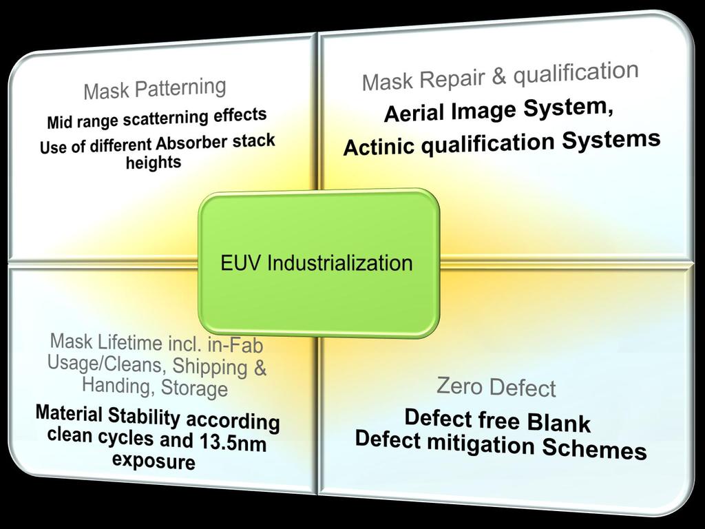
2 EUV Masks Challenge Pyramid Zero defect printability needs a lot of Mask supporting infrastructure HVM Storage Mask Lifetime Mask in-fab Use & Handling Defect Free Shipping &Handing Inspection, Repair and Phase Defect compensation Absorber patterning process with black border Defect mitigation by pattern shift/ blank rotation Low defect mask blanks with Fiducials (Location accuracy)
3 EUV Mask Manufacturing flow-what is different? Blank Supplier* Mask Shop * Assumes fiducials blanks New Mask Data- OPC Flare, HV bias?? Blank Sorting Pattern Shift Blank orientation. Pattern Generator New Shift /Rotation Litho(e-beam) Confirmation (Coat/Bakes/Develop) Resist CD Metrology Absorber etch Resist strip New In Fab Handling NXE Exposure New BB Placement Metrology BB loop Metrology Litho(Alta)/ML etch/ Strip/Clean Repair/ Clean Clean Inspection Transfer/Shuffler to DP Redo loop (Optional) Storage Ship DP or RSP Final Audit Clean Inspection Redo loop (Optional) Transfer/Shuffler To DP/Ship Box New EUV AIMS Back Side Insp BB Repair (incl Comp) /Clean


4 Mask Blank Gaps/Challenges Fiducial Strategy and Blank Supply with fiducials SEMI P-48 task force Defect location accuracy relative to fidcuials Upfront Identification of blank defects that print Defects > 100nm Difficult to hide/repair by defect mitigation approach Primary cause is deposition process
5 Defect mitigation Pattern Shift
6 Fiducial SEMI P-48 draft under reconsideration


7 Fiducial SEMI P-48 draft Supplier prespective
 or fill region Identify critical area for defect hiding on the layout Printed without Repair; Only 1 repairable defect")
8 20nm Integration Mask defect printability result Integration flows showing promising results for early confidence building but will not be sufficient For HVM Blank Sorting vs layout Blank orientation and pattern shift selection to hide blank defects under absorber (dark pattern) or fill region Identify critical area for defect hiding on the layout Printed without Repair; Only 1 repairable defect in critical area

")


 [nm] <2.6 <5.")

9 Mask Process Mask Preparation Customer Design Mask Manufacture Resist coat and bake Expose (and bake ) Develop Etch Strip Data Preparation EUV Mask Process achieves CD control Mask verification Meet targets for CD and Placement CD- Metrology Registration- Metrology Defect- Inspection Defect-Repair Repair- Qualification Clean Mask shipping Deal w/ EUV specific effects Parameter on Mask level CD-Uniformity (3s) (dense) Linearity (60-400nm) [nm] <2.6 <5.5 Image Placement (3s) <5 SEM images of cross sections 60nm Dense Lines 40nm Isolated Clear 70nm Isolated dark 9
10 Average CD Error (Mask Scale 4x nm) Energy (ev/um 3 ) Mask Process -MPC EUV Electron Backscatter Electron backscatter from EUV mask blank material large compared to DUV masks This causes short range variation in printing Worst Case Example: Through pitch variation of absorber line Variation MUCH larger than 0.3nm error allowance Not corrected by state of the art mask writers Not (explicitly) modeled in OPC 1, Absorbed Energy in Resist (Simulated) MPC Cr OMOG EUV Radius (um) Monte Carlo Simulation Performed with PENELOPE Absorber Line Through Pitch Avg. CD Error vs. Pitch CD 11 nm Linearity Error Measured Mask Data Pitch (Wafer Scale 1x nm)

11 Evaluation of MPC solutions CD Control of small spaces estimated to be most crucial Only few solutions able to provide reasonable control Correction capability for lines much better throughout all models Need better performance towards 7nm node AMTC and GF continue to drive selected suppliers to improve capabilities


12 Black Border-Added Challenges Additional mask process steps - added Cycle time and Mask process challenges Impacts 2 nd Patterning Process Step to remove Border with well controlled reflectivity at 13.5nm <0.05% and sidewalls Defect Inspection within BB area Defect Inspection proximity to BB Area Role of cleans for mask lifetime Impact on CD Metrology (ESD/CD drift) T. Katai et. al, PMJ 2013

13 Mask Cleans- Maximizing Lifetime is essential Target >100 clean Cycles Opportunity for Dry Cleans to maximize lifetime Suss Mircotec Key Parameters: Ru Surface Roughness, Absorber Modification, Absorber CD control, EUV reflectivity, Front and Backside PRE

 Nano")


14 Defect Repair Defects Types Repairable thru standard techniques Particles Process Defects (clear/dark) Nano Machining Focus ion Beam Nano machining Defect before Repair after Repair Diamond-Tip CD SEM AFM scan AFM scan Focused Ion beam (FIB) Gas Injector Focused Ion Beam Charge Neutralizer Vacuum Chamber CD SEM CD SEM

15 Defect Mitigation Compensation Repair for ML-Defect Defects Types Compensation Repair Process Defects (clear/dark) Repair of Multilayer defects by compensation of ML introduced error on Wafer Multilayer Defect can not be detected by standard mask inspection technology Wafer print thru focus of Multilayer Defect showed clear impact on imaging Bump of 7nm found by AFM Repair qualification: For optical Mask use of AIMS (Aerial Image Microscope) to verify repaired defect sites For EUV Mask no AIMS until 2014 available Verification of repairs have to be done by wafer prints or alternative approaches

16 Mask defectivity: Handling & Defects No EUV pellicle exists today EUV pellicle solutions are being explored again, to help mitigate the defect challenge Dual Pod solution as alternative available Potentially defect & contamination origin Electrostatic chucking in EUV-Scanner Shipping Handling Storage Cleaning can improve lifetime of Mask at point of use O. Wood, GlobalFoundries, EUV Litho Symposium, 2010

17 Mask defectivity : Challenge on Back Side after exposure back side µm µm µm µm µm µm µm After clamp and clean µm µm µm µm µm µm µm

18 1 absorption length (nm)-1 New Opportunities-EUV masks Thin absorber Essential for EUV Extensibility HV Bias, Telecentricity (PP) Meet all current absorber requirements inc. Plasma etching Cleaning, Inspection, Repair Durability under exposure. Pellicle development Significant progress shown Need full integrated solution Adhesive, Outgassing Frame definition Inspection strategy Ni Ag Te Ta Levinson, SPIE 2013


19 EUV Masks Challenge Summary Zero defect printability needs a lot of Mask supporting infrastructure HVM Storage Mask Lifetime Mask in-fab Use & Handling (No pellicle) Defect Free Shipping &Handing Inspection, Repair and Phase Defect compensation, EUV AIMS Absorber patterning process with black border Defect mitigation by pattern shift/ blank rotation Low defect mask blanks with Fiducials (with defct Location accuracy)
20 Summary

21 Questions? AMTC is a joint Venture of GLOBALFOUNDRIES and TOPPAN Photomask