Smart PCBs. Work
|
|
|
- Brent Dean
- 5 years ago
- Views:
Transcription
 51 457 8047, Fax (0) 51 457 8048 www.smartpcbs.")
1 0 Smart PCBs Service Road, Shaheen Town, near Airport Chowk, Rawalpindi, 4600, PAKISTAN Tel: +92 (0) , Fax (0)
2 Dear Sir/Madam, SmartPCBs is the leading fabricators of printed circuit boards (PCBs) in Pakistan, capable of manufacturing single, double, and multilayer PCB s. The company differentiates itself with other competitors in experienced workforce, superior quality, and advanced equipment. Our multifaceted approach to production in terms of engineering prototypes and bulk orders of single and multilayer PCB s offer our customers a wide range of flexibility and options. This enables us to develop solutions which allow our clients to increase productivity, reduce operating costs and increased customer satisfaction. Moreover, SmartPCBs offer its customers with sustainable competitive advantage of products showing complete commitment from initial quotation to delivery of order and beyond. Please take a few minutes to read the enclosed brochure. See how SmartPCB'can optimize your manufacturing needs for PCBs both at the production & prototype level. I invite you to contact us so that we can discuss in details how we can help you. Thank you of the interest that you have shown in SmartPCBs. Looking forward to hear from you soon. With all the best regards. S. M. Adnan Iqbal GM, SmartPCBs, Cell: Cell: marketing@smartpcbs.com smartpcbs@hotmail.com

3
4 Smart PCBs Smart PCBs was founded in 2006, is one of the leading fabricators of printed circuit boards in Pakistan, capable of manufacturing single, double, and multilayer PCBs. The company differentiates itself with other competitors in experienced workforce, superior quality, and advanced equipm ent. Our multifaceted approach to production in terms of engineering prototypes and bulk orders of single and multilayer PCBs offer our customers a wide range of flexibility and options.
5 PRODUCTION PARAMETERS S.No Description Manufacturing Value 1 GENERAL PARAMETERS Substrate (Customer material is acceptable) FR4, FR2, CEM 2 Substrate TG C (As per Customer requirement) 135 & Type of PCB (Flex: Only single side without drill) Rigid/Flexible 4 Max. Number of Layers 16 5 PCB Size (inxin) - Single & Double Sided PCB 12 X 15 6 PCB Size (inxin) - Multilayer PCB 9.5 X 15 7 PCB Thickness (mm) PRODUCTION PARAMETERS Copper Thickness 35 micron 17 micron 8 Track to Track Outer layer clearance (mil) 9 Track to Track Inner layer clearance (mil) 10 Track to Pad clearance outer Layer (mil) 11 Track to Pad clearance inner Layer (mil) Pad to Pad clearance (mil) 13 Minimum Component Pitch (mil) 14 Minimum Track Width Outer Layer (mil) Minimum Track Width Inner Layer (mil) Minimum Anular Ring (mil) Minimum FPGA pad DIA (mil) Minimum Board Edge to Conductor (mm) Minimum Dielectric Thickness (mm) CNC DRILLING/ROUTING PARAMETERS 20 Minimum Hole/Drill Size (mm) Maximum Hole/Drill Size (mm) Minimum PCB Size (inxin) 0.67 x Minimum Two Drill Hole Distance (mil) 5 24 Drill Hole to Inner Layer Track clearance (mil) Minimum NPTH, PTH Slot width (mm) 1 26 Aspect Ratio (Board Thicknes to Drill Hole Ratio) 6 : 1 27 Pad & Track to Copper Sheilding Clearance (mil) V-cut width (cutting range from edge to V-cut) - min & max (in) 0.75 & V-cut PCB size - min & max (inxin) 6x6 & 12x12 30 For Tab Route, Min. PCB to PCB Distance (mm) 5 31 For Tab Route, Min. PCB to Outer Edge (mm) 7 32 SURFACE FINISH PARAMETERS Surface Finish HASL, FINGER GOLD, ENIG 33 Solder Mask Clearance (mil) 6 34 Minimum Solder Mask ring (mil) 4 35 Legend Component Designator & Writing Clearance from SMT Pads (mil) Legend Character Height (mm) - Color White 1mm 37 Legend Character Apperture (mil) 7 SPECIAL REQUIREMENTS 38 Burried Vias (for R&D purpose) Possible 39 Blind Vias Not available 40 Impedence Measurement Not available 41 SMT SERVICES For Prototypes, Low & High-mix SMT Production Min: 0.4X0.2 (01005) 42 Component Size (mm) Max: 80X70 43 Height: PCB Size (mm) 600X560 QUALITY STANDARDS IPC-6012D, IPC600J REMARKS Any specifcation over and above may please be discussed with Smart PCBs for taking the project as R&D


6 Production Environment Dry Film Pre Treatment Screen Printing Dry Film Exposing CNC Drilling
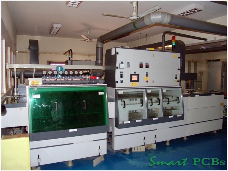
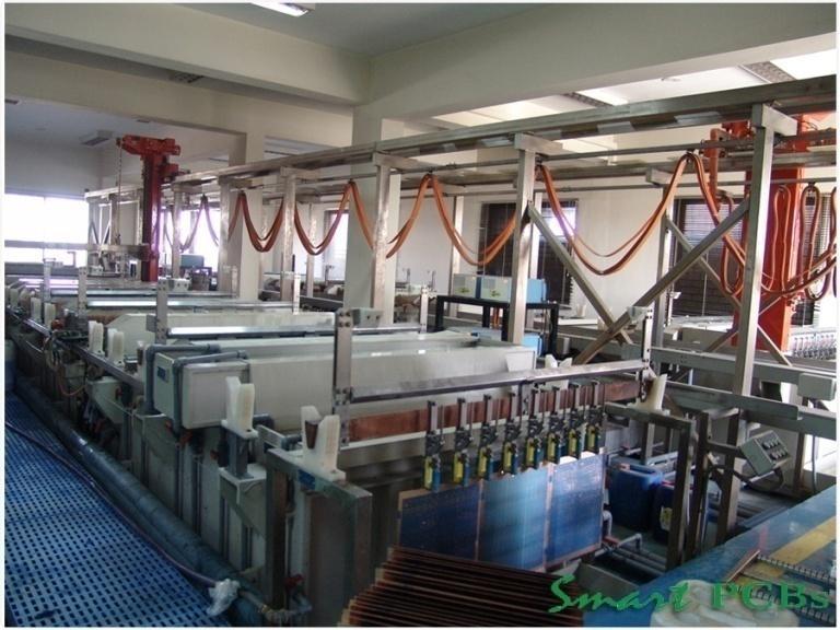
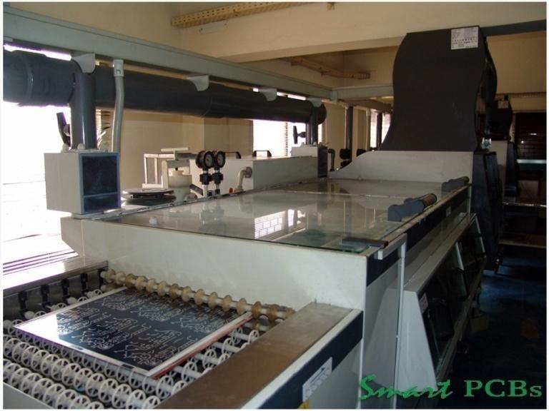
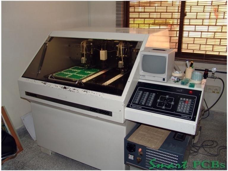
7 Dry Film Developing Pattern Plating Line Film Stripping CNC Routing


8 Multi Layer Press Flying Prob Tester Automatic Optical Inspection Solder Mask Exposing
9 Our strategic plan is to provide our customers with sustainable competitive advantage of our products showing complete commitment from initial quotation to delivery of order and beyond. Moreover, this assures our customers that SmartPCBs continues to meet the quality conscious approach they have grown to expect. Contact Person S. M. Adnan Iqbal General Manager Tel: +92 (0) Fax: +92 (0) Cell: +92 (0) Cell: +92 (0) SmartPCBs. In the interest of constant product improvement, specifications are subject to change without notice.