1.0A Single-chip Li-ion and Li-POL Charger with OVP Protection
|
|
|
- Rudolph Collins
- 5 years ago
- Views:
Transcription
1 1.0A Single-chip Li-ion and Li-POL Charger with OVP Protection General Description The /A is a complete constant-current/ constant voltage linear charger for single cell lithium-ion batteries. Its TDFN-10 package and low external component count make the /A ideally suited for portable applications. No external sense resistor is needed, and no blocking diode is required due to the internal MOSFET architecture. Thermal feedback regulates the charge current to limit the die temperature during high power operation or high ambient temperature. The charge voltage is fixed at 4.2V/4.35V, and the charge current can be rammed externally with a single resistor(ribat). The automatically terminates the charge cycle when the charge current drops to 1/10th the RIBAT rammed value after the final float voltage is reached. When the input supply is removed, the /A automatically enters a low current state, dropping the battery drain current to less than 1µA. Other features include charge current monitor, under voltage lockout, automatic recharge and a status pin to indicate charge termination and the presence of an input voltage. Order Information BAT Voltage Default: 4.2V 43: 4.35V F: Pb-Free Package Type QV: TDFN-10 SP: ESOP8 Function Class Default:OCP Adjustable A:Enable Features Very Low Power Dissipation Input Voltage: 3.8V~36V Input OVP: 6.1V Protection of Reverse Connection of Battery Programmable Charge Current Up to 1000mA No MOSFET, Sense Resistor or Blocking Diode Required Constant-Current/Constant-Voltage Operation with Thermal Regulation to Maximize Charge Rate Without Risk of Overheating 1µA Leakage Current in Shutdown Drainage Charge Current Thermal Regulation Status Outputs for LED or System Interface Indicates Charge and Fault Conditions Consumption Available in TDFN-10 Package RoHS Compliant and 100% Lead (Pb)-Free Applications Portable Media Players/Game Power Bank PDA/MID Bluetooth Applications Marking Information Device Marking Package Shipping A LPS YWX LPS Marking indication: A YWX QV:TDFN-10 SP:ESOP8 QV:TDFN-10 3K/REEL 2.5K/REEL 3K/REEL Y:Production year W:Production week X: Series Number -04 Apr marketing@lowpowersemi.com Page 1 of 11
2 Typical Application Circuit CIN 1uF OV 2K Battery VBAT LED1 CBAT 10uF ILIMIT LED2 RLIMIT RIBAT A CIN 1uF OV 2K OFF Battery ON EN VBAT LED1 LED2 CBAT 10uF RIBAT Functional Pin Description Package Type Pin Configurations ILIMIT ESOP8 / TDFN-10 () BAT ILIMIT BAT OV ESOP8 TDFN-10 TDFN-10 (A) EN BAT TDFN OV -04 Apr marketing@lowpowersemi.com Page 2 of 11
3 Pin Description Pin A Name Description ESOP8 TDFN-10 TDFN-10 6,9 1,7,11 1,7,11 is the connection to system ground. 1 2 ILIMIT Input Current limit Program Pin. The input current from to OV is programmed by connecting a 1% resistor(rlimit)to ground. 2 /EN Chip enable pin. Active low BAT BAT is the connection to the battery Open-Drain Charge Status Output. When the battery is charging, this pin is pulled High by an internal N-channel MOSFET. When the charge cycle is completed, the pin is pulled Low Open-Drain Charge Status Output. When the battery is charging, this pin is pulled low by an internal N-channel MOSFET. When the charge cycle is completed, the pin is pulled High Charge Current Program, Charge Current Monitor and Shutdown Pin Input of Charger. Connect a capacitor 10uF to ground. 9 9 OV Output of Over Voltage Protection part. Connect a capacitor 10uF to ground is the input power source with Over Voltage Protection part. Connect to a wall adapter. -04 Apr marketing@lowpowersemi.com Page 3 of 11
4 Function Diagram OV Charge pump OCP Control Logic ILIMIT EN Vref 145 TDIE TA OTP 1X X NC TTEMP MA 5μA R1 BAT TTEMP CA - + VA % SHDN C1 - + R3 1V R4 REF 1.22V R2 C V R5 C3 + - TO BAT 2.9V 3μA VCC -04 Apr marketing@lowpowersemi.com Page 4 of 11
5 Absolute Maximum Ratings Note 1 Input Voltage to () V to 36V, V Voltage to (,OV) V to 7V BAT to V to 8V to BAT V BAT Short-Circuit Duration Continuous BAT Pin Current mA Other pin to V to 6V Maximum Junction Temperature Operating Ambient Temperature Range(T A) to 85 Storage Temperature to 165 Maximum Soldering Temperature (at leads, 10 sec) Note 1. Stresses beyond those listed under Absolute Maximum Ratings may cause permanent damage to the device. These are stress ratings only, and functional operation of the device at these or any other conditions beyond those indicated in the operational sections of the specifications is not implied. Exposure to absolute maximum rating conditions for extended periods may affect device reliability. Thermal Information Maximum Power Dissipation (P D, T A=25, TDFN-10) W Maximum Power Dissipation (P D, T A=25, ESOP8) W Thermal Resistance (J A,TDFN-10) /W Thermal Resistance (J A,ESOP8) /W ESD Susceptibility HBM(Human Body Mode) KV MM(Machine Mode) V -04 Apr marketing@lowpowersemi.com Page 5 of 11
6 Electrical Characteristics (T A=25. V IN=5V, unless otherwise noted.) Symbol Parameter Condition Min Typ Max Units Input Voltage V VP OVP threshold increasing from 5~7V V VHYS-OVP OVP hysteresis decreasing from 7~5V 150 mv TOVP OVP active time =5->10V 1 μs TON(OVP) OVP recovery time =10->5V to output ON 9 ms RLIMIT=51K 1.9 A ILIMIT Input current limit set () RLIMIT=82K 1.3 A RLIMIT=150K 0.85 A RLIMIT=NC A TOCP Over current Protection detection time 30 ms VILIMIT ILIMIT Voltage 0.8 V TON(OCP) Over current Protection recovery time 1 s VEN(ON) Chip enable 0.4 V (A) VEN(OFF) Chip shutdown 1.4 V Charge Mode, RIBAT=10k μa IQ Input Supply Current Standby Mode (Charge Terminated) μa VFLOAT Regulated Output (Float) Voltage IBAT=40mA(XXX) V IBAT=40mA(XXX-43) V RIBAT=1k, Current Mode 1000 ma RIBAT=2k, Current Mode 500 ma IBAT BAT Pin Current Standby Mode, VBAT=4.2V μa Shutdown Mode (RIBAT NC) ±1 ±2 μa Reverse Current, VBAT=-4.2V -1 ma ITRIKL Trickle Charge Current VBAT<2.8V 30 ma VTRIKL Trickle Charge Threshold Voltage RIBAT=10k, VBAT Rising V VTRHYS Trickle Charge Hysteresis Voltage RIBAT=10k 120 mv VUV Under voltage Lockout Threshold V from Low to High 3.8 V VUVHYS Under voltage Lockout Hysteresis 500 mv VASD V VBAT Lockout Threshold Voltage V from Low to High 100 mv V from High to Low 80 mv ITERM C/10 Termination Current Threshold RIBAT = 10k 10 %IBAT RIBAT = 2k 10 %IBAT V IBAT Pin Voltage RIBAT=10k, Current Mode 1 V I(/) / Pin Weak Pull-Down Current V(/)= 5V 5 μa V(/) / Pin Output Low Voltage I(/)=5mA V ΔVRE Recharge Battery Threshold Voltage VFLOAT-VRE mv TLIM Junction Temperature in Constant Temperature Mode 150 ΔTLIM OTP hysteresis 20 RON Power FET ON Resistance (Between and BAT) 300 mω -04 Apr marketing@lowpowersemi.com Page 6 of 11


7 Typical Operating Characteristics of OVP Turn on waveform OVP waveform V IN falling waveform OCP detection time -04 Apr marketing@lowpowersemi.com Page 7 of 11
8 Application Information The is a single cell lithium-ion battery charger using a constant-current/constant-voltage algorithm. It can deliver up to 1000mA of charge current (using a good thermal PCB layout) with a final float voltage accuracy of ±1%. The includes an internal P-channel power MOSFET and thermal regulation circuitry. No blocking diode or external current sense resistor is required; thus, the basic charger circuit requires only two external components. Furthermore, the is capable of operating from a USB power source. Charge Termination A charge cycle is terminated when the charge current falls to 1/10th the rammed value after the final float voltage is reached. This condition is detected by using an internal, filtered comparator to monitor the pin. When the pin voltage falls below 200mV for longer than tterm(typically 1ms), charging is terminated. The charge current is latched off and the LP28056S enters standby mode, where the input supply current drops to 200µA. In this state, all loads on the BAT pin must be supplied by the battery. (Note: C/10 termination is disabled in trickle charging and thermal limiting modes). Normal Charge Cycle A charge cycle begins when the voltage at the pin rises above the UVLO threshold level and a 1% resistor is connected from the pin to ground or when a battery is connected to the charger output. If the BAT pin is less than 2.8V, the charger enters trickle charge mode. In this mode, the supplies 30mA charge current to bring the battery voltage up to a safe level for full current charging. When the BAT pin voltage rises above 2.9V, the charger enters constant-current mode, where the R rammed charge current is supplied to the battery. When the BAT pin approaches the final float voltage, the enters constant-voltage mode and the charge current begins to decrease. The charge cycle ends when the charge current drops to 1/10 of the R rammed value. ramming Charge Current The charge current is I IBAT rammed using a single resistor from the pin to ground. The battery charge current is 1000 times the current out of the I IBAT pin. The I IBAT ram resistor and the charge current are calculated using the following equations: R =1000V/I BAT I BAT= 1000V/R The charge current out of the BAT pin can be determined at any time by monitoring the IBAT pin voltage using the following equation: I BAT=V 1000/R Note: V IBAT is 1Volts. -04 Apr marketing@lowpowersemi.com Page 8 of 11
9 Thermal Limiting An internal thermal feedback loop reduces the IBAT rammed charge current if the die temperature attempts to rise above a preset value of approximately 150. This feature protects the from excessive temperature and allows the user to push the limits of the power handling capability of a given circuit board without risk of damaging the. The charge current can be set according to typical (not worst-case) ambient temperature with the assurance that the charger will automatically reduce the current in worst-case conditions. TDFN power considerations are discussed further in the Applications Information section. Charge Status Indicator The charge status output has two different states: strong pull-down (~5mA) and high impedance. The strong pull-down state indicates that the is in a charge cycle. Once the charge cycle has terminated, the pin state is determined by under voltage lockout conditions. High impedance indicates that the is in under voltage lockout mode: either is less than 100mV above the BAT pin voltage or insufficient voltage is applied to the pin. A microprocessor can be used to distinguish between these two states this method is discussed in the Applications Information section. When rise above 6.1V(typ.), the and LEDs would be turned off. A microprocessor can be used to distinguish between these two states. Function Charging low high Charge Complete high low -04 Apr marketing@lowpowersemi.com Page 9 of 11


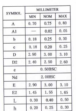
10 Packaging Information TDFN Apr Page 10 of 11

11 ESOP8-04 Apr Page 11 of 11