LASER MICROMACHINING A New Tool for Precision Engineers
|
|
|
- Shavonne Dickerson
- 6 years ago
- Views:
Transcription
")
1 LASER MICROMACHINING A New Tool for Precision Engineers Nadeem Rizvi UK Laser Micromachining Centre Laser Applications for Micro and Nano Engineering AILU Workshop 14 June 2006 (Oxford)

2 FOCUS ON MICRO & NANOTECHNOLOGY Major push in MNT sectors. DTI and RDAs investing heavily in supporting microfabrication. UK-LMC established in 2005 as the national Centre of Excellence for laser micromachining. Primary aim of UK-LMC is to provide laser micromachining services to UK industry and research: - Commercial service - Fast Response - No Job Too Small UK-LMC: wide customer base covering many sectors in UK and Europe. Experience of working with large companies, SMEs, research centres. MNT is an umbrella covering many technologies Precision is the key.
3 TYPCIAL MNT CUSTOMERS REQUIREMENTS EXPECTATIONS Materials: glass, polymers, silicon, thin metals, thin films, composites. Features: holes, slots, channels, complex shapes in 2D/3D parts. Quality: high precision, tight tolerances, precise control. Dimensions: ~1um to ~500um. Produce desired features in selected materials to design specification and deliver high quality finished article. Fast turnaround, competitive prices, 1off to larger numbers. Novel designs and product ideas make something for the first time. Basic demands are similar to traditional users of laser machining except for smaller features, tighter tolerances and wider range of materials.
4 FABRICATION TRENDS Nano tag on many products, fabrication of most parts on micro scale. Traditional precision products are extending into the micro domain. FABRICATION NEEDS NANO MICRO MACRO MNT companies require microfabrication MNT-PRECISION LASER JOB SHOP Non-MNT companies require precision parts


5 LASER JOB SHOPS TRADITIONAL Well-established. >100 in UK. Highly competitive market. Integral part of supply chains. Pressures on pricing. Fast turnaround for standard jobs. Mainly metal cutting & welding. MNT-PRECISION Relatively new. ~6 in UK. Niche expertise areas. Diverse customers. Work gained by level of expertise. Delivery governed by complexity and novelty. Any material. Operating model for traditional job shops can be applied to MNT-Precision sectors as demand grows.
6 ROUTE TO MANUFACTURE - 1 DESIGN Material choice. Tolerances. Quality issues. Manufacturability. Design of part to be made

7 ROUTE TO MANUFACTURE - 2 CONVERSION Transfer design into suitable format. Account for laser machining process. Decide on type of laser and method of machining. Laser cut paths defined


8 ROUTE TO MANUFACTURE - 3 MACHINING Set-up laser tool. Optimise process for job requirements. Produce parts. Finished part in 25um stainless steel 1mm 100um

9 PRECISION JOB SHOP SERVICE Complete service from design advice, process optimisation, production. Quote for work (price, deliverables, completion time). Deliver parts on time according to quote, including report on work with pictures of results. Service includes free advice on design and manufacturing options.

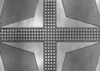
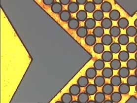
10 MICROELECTRODES SENSORS High resolution patterning of complex features. Demetallisation of 30nm gold on glass. Electrode pattern is ~4mm x 3mm Rapid, scalable technique for the production of multiple samples. VIDEO 10um gap Sectors: Microelectronics, Sensors, Biotech
11 MICROMACHINING OF POLYMERS 150um holes VIDEO Sectors: Biomedical, Electronics

12 MICROFLUIDIC DEVICES 50µm wide x 45µm deep microchannels in polycarbonate Ideal for rapid evaluation of different designs. Highly flexible technique. No requirement for new masks for each stage. VIDEO Sectors: Medical, Biotech, Nanoparticles


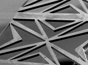
13 MACHINING EXPERTISE Slots in Ø125um fibre Ø50um microlenses in polymer 50um wide bars in nickel Precision tasks, Standard service Cutting of 6 silicon wafer
14 SUMMARY Precision engineers can now expect the same laser micromachining service as that provided by traditional laser job shops. Fabrication demands and needs of MNT and Precision users are very similar. Traditional laser job shop model can be applied to the MNT- Precision sectors. Ease of access and high-quality service provision are extending the uses of lasers into new areas. Contact: Nadeem Rizvi
Applications of High-Performance MEMS Pressure Sensors Based on Dissolved Wafer Process
 Applications of High-Performance MEMS Pressure Sensors Based on Dissolved Wafer Process Srinivas Tadigadapa and Sonbol Massoud-Ansari Integrated Sensing Systems (ISSYS) Inc., 387 Airport Industrial Drive,
LOW TEMPERATURE PHOTONIC SINTERING FOR PRINTED ELECTRONICS. Dr. Saad Ahmed XENON Corporation November 19, 2015
 LOW TEMPERATURE PHOTONIC SINTERING FOR PRINTED ELECTRONICS Dr. Saad Ahmed XENON Corporation November 19, 2015 Topics Introduction to Pulsed Light Photonic sintering for Printed Electronics R&D Tools for
Innovative Laser Processing Technologies
 Innovative Laser Processing Technologies Reinhard Ferstl Director Sales & Marketing EMEA / Asia Corning Laser Technologies September 21, 2016 2016 Corning Incorporated Corning Market Segments and Additional
Leveraging the Precision of Electroforming over Alternative Processes When Developing Nano-scale Structures
 VOLUME 4 - ELECTROFORMING Leveraging the Precision of over Alternative Processes When Developing Nano-scale Structures Electrical and mechanical component and subsystem designers generally have five techniques
Nanoimprinting in Polymers and Applications in Cell Studies. Albert F. YEE Chemical Engineering & Materials Science UC Irvine
 Nanoimprinting in Polymers and Applications in Cell Studies Albert F. YEE Chemical Engineering & Materials Science UC Irvine Presentation outline Motivation Reversal imprinting Soft inkpad imprinting on
Micro and nano structuring of carbon based materials for micro injection moulding and hot embossing
 Micro and nano structuring of carbon based materials for micro injection moulding and hot embossing Victor Usov, Graham Cross, Neal O Hara, Declan Scanlan, Sander Paulen, Chris de Ruijter, Daniel Vlasveld,
Large Area Functional Surfaces By Roll-to-Roll Nanoimprint Lithography Project: APPOLO
 Large Area Functional Surfaces By Roll-to-Roll Nanoimprint Lithography Project: APPOLO Mr. Theodoros Tachtsidis Nanotypos 23rd and 24th of June Amsterdam Core Overview Nanotypos is a pioneering research
Lecture 19 Microfabrication 4/1/03 Prof. Andy Neureuther
 EECS 40 Spring 2003 Lecture 19 Microfabrication 4/1/03 Prof. ndy Neureuther How are Integrated Circuits made? Silicon wafers Oxide formation by growth or deposition Other films Pattern transfer by lithography
Challenges for Embedded Device Technologies for Package Level Integration
 Challenges for Embedded Device Technologies for Package Level Integration Kevin Cannon, Steve Riches Tribus-D Ltd Guangbin Dou, Andrew Holmes Imperial College London Embedded Die Technology IMAPS-UK/NMI
ADVANCING ADDITIVE MANUFACTURING IN AEROSPACE AM-AERO14
 ADVANCING ADDITIVE MANUFACTURING IN AEROSPACE AM-AERO14 ADDITIVE MANUFACTURING Aerospace is leading the way in adopting additive manufacturing (AM) for the manufacturing industry. AM allows aerospace manufacturers
Lecture 5. SOI Micromachining. SOI MUMPs. SOI Micromachining. Silicon-on-Insulator Microstructures. Agenda:
 EEL6935 Advanced MEMS (Spring 2005) Instructor: Dr. Huikai Xie SOI Micromachining Agenda: SOI Micromachining SOI MUMPs Multi-level structures Lecture 5 Silicon-on-Insulator Microstructures Single-crystal
Learning about the nanoscale and the SI system of measurement
 NNIN Nanotechnology Education Learning about the nanoscale and the SI system of measurement Student Worksheet Materials candy assorted sizes coins assorted sizes Metric ruler NanoRuler Paper pencil, construction
Mater. Res. Soc. Symp. Proc. Vol Materials Research Society
 Mater. Res. Soc. Symp. Proc. Vol. 940 2006 Materials Research Society 0940-P13-12 A Novel Fabrication Technique for Developing Metal Nanodroplet Arrays Christopher Edgar, Chad Johns, and M. Saif Islam
Tackling the optical interconnection challenge for the Integrated Photonics Revolution
 Tackling the optical interconnection challenge for the Integrated Photonics Revolution Dr. Ir. TU Delft, Precision and Microsystems Engineering m.tichem@tudelft.nl Microfabrication and MEMS Si microfabrication
EXPLORING VACUUM CASTING TECHNIQUES FOR MICRON AND SUBMICRON FEATURES. Campus Ker Lann, av Robert Schumann Bruz, France
 EXPLORING VACUUM CASTING TECHNIQUES FOR MICRON AND SUBMICRON FEATURES M. Denoual *, P. Mognol **, B. Lepioufle * * Biomis-SATIE ENS-Cachan antenne de Bretagne, Campus Ker Lann, av Robert Schumann 35170
High-throughput three-dimensional (3D) lithographic microfabrication in biomedical applications
 lithographic microfabrication in biomedical applications") High-throughput three-dimensional (3D) lithographic microfabrication in biomedical applications The MIT Faculty has made this article openly available. Please share how this access benefits you. Your story
High-throughput three-dimensional (3D) lithographic microfabrication in biomedical applications The MIT Faculty has made this article openly available. Please share how this access benefits you. Your story
A Microtensiometer for Large-Range Measurement of Water Potential in Plants, Soils and Other Materials
 School of Chemical and Biomolecular Engineering A Microtensiometer for Large-Range Measurement of Water Potential in Plants, Soils and Other Materials Vinay Pagay, Alan Lakso, and Abraham Stroock Departments
Multiphoton lithography based 3D micro/nano printing Dr Qin Hu
 Multiphoton lithography based 3D micro/nano printing Dr Qin Hu EPSRC Centre for Innovative Manufacturing in Additive Manufacturing University of Nottingham Multiphoton lithography Also known as direct
Biomedical sensor technology: state - of the art and future roadmap
 Biomedical sensor technology: state - of the art and future roadmap Ralph W. Bernstein SINTEF Microsystems and nanotechnology 1 MiNaLab Clean room area: SINTEF: 800 m 2 University of Oslo: 600 m 2 Micro
Surface micromachining and Process flow part 1
 Surface micromachining and Process flow part 1 Identify the basic steps of a generic surface micromachining process Identify the critical requirements needed to create a MEMS using surface micromachining
Advances in Intense Pulsed Light Solutions For Display Manufacturing. XENON Corporation Dr. Saad Ahmed Japan IDW 2016
 Advances in Intense Pulsed Light Solutions For Display Manufacturing XENON Corporation Dr. Saad Ahmed Japan IDW 2016 Talk Outline Introduction to Pulsed Light Applications in Display UV Curing Applications
3D inkjet printing of conductive structures using in-situ IR sintering
 3D inkjet printing of conductive structures using in-situ IR sintering E. Saleh*, J. Vaithilingam, C. Tuck, R. Wildman, I. Ashcroft, R. Hague, P. Dickens University of Nottingham, Additive Manufacturing
In-Situ Monitoring of Pattern Filling in Nano-Imprint Lithography Using Surface Plasmon Resonance
 Copyright 2011 American Scientific Publishers All rights reserved Printed in the United States of America Journal of Nanoscience and Nanotechnology Vol. 11, 1 6, 2011 In-Situ Monitoring of Pattern Filling
Producing Metal Parts
 Producing Metal Parts CNC vs. Additive Manufacturing www.3dhubs.com METAL KIT 2 Introduction This Kit discusses how to select the right manufacturing process for metal parts by comparing CNC and Additive
BOROFLOAT & Glass Wafers: A Union of Inspiration & Quality
 Home Tech SCHOTT North America, Inc. 553 Shepherdsville Road Louisville, KY 4228 USA Phone: +1 (52) 657-4417 Fax: +1 (52) 966-4976 Email: borofloat@us.schott.com www.us.schott.com/borofloat/wafer BOROFLOAT
Engel Diversified Industries Inc.
 Engel Diversified Industries Inc. PO Box 85 1060 Quaker Avenue Jordan, MN 55352 Represented by: Duane Jaworski & Associates 763-792-2184 Toll Free 877-562-5070 Fax 763-785-9065 Toll Free 877-280-2087 EDi
Vacuum casting, a new answer for manufacturing biomicrosystems
 1 Vacuum casting, a new answer for manufacturing biomicrosystems M Denoual 1 *, P Mognol 2, and B Lepioufle 1 1 Biomis-SATIE ENS-Cachan antenne de Bretagne, Bruz, France 2 IRCCyN Nantes, France The manuscript
KARIM FORESIGHTING ON MICROINJECTION MOULDING TECHNOLOGY
 Karim Market Report: Opportunities for European SMEs Demonstrator microfluidics component and Ra plot of moulded surface (6nm baseline) KARIM KARIM FORESIGHTING ON MICROINJECTION MOULDING TECHNOLOGY Executive
Photonic Drying Pulsed Light as a low Temperature Sintering Process
 Photonic Drying Pulsed Light as a low Temperature Sintering Process Lou Panico Xenon Corporation W E S T E R N M I C H I G A N U N I V E R S I T Y PRESENTATION OVERVIEW What is Printed Electronics Materials
Superionic Solid State Stamping (S4)
") Superionic Solid State Stamping (S4) Lead Faculty Researcher: Placid Ferreira Department: Materials Science & Engineering Hsu et al, Nano Letters, 2007 1. Description: This dry, single step, electrochemical
Superionic Solid State Stamping (S4) Lead Faculty Researcher: Placid Ferreira Department: Materials Science & Engineering Hsu et al, Nano Letters, 2007 1. Description: This dry, single step, electrochemical
Implantable Microelectronic Devices
 ECE 8803/4803 Implantable Microelectronic Devices Fall - 2015 Maysam Ghovanloo (mgh@gatech.edu) School of Electrical and Computer Engineering Georgia Institute of Technology 2015 Maysam Ghovanloo 1 Outline
NovoPlan. The Coating Experts. PlanoTek Functional layers. Quality. Perfection. Expertise. Consulting
 The Coating Experts NovoPlan Quality Perfection Expertise Consulting PlanoTek Functional layers for plastics processors, injection moulders, tool and mould makers and mechanical engineers PlanoTek The
ALTERNATIVES TO SOLDER IN INTERCONNECT, PACKAGING, AND ASSEMBLY
 ALTERNATIVES TO SOLDER IN INTERCONNECT, PACKAGING, AND ASSEMBLY Herbert J. Neuhaus, Ph.D., and Charles E. Bauer, Ph.D. TechLead Corporation Portland, OR, USA herb.neuhaus@techleadcorp.com ABSTRACT Solder
Conveyor System Technology. krones AirCo. Air Conveyor
 Conveyor System Technology krones AirCo Air Conveyor Gentle Product Conveyance The krones AirCo conveyor links the systems of a bottling line, and provides an important integral part of a smoothly running
Photolithography I ( Part 2 )
") 1 Photolithography I ( Part 2 ) Chapter 13 : Semiconductor Manufacturing Technology by M. Quirk & J. Serda Bjørn-Ove Fimland, Department of Electronics and Telecommunication, Norwegian University of Science
1 Photolithography I ( Part 2 ) Chapter 13 : Semiconductor Manufacturing Technology by M. Quirk & J. Serda Bjørn-Ove Fimland, Department of Electronics and Telecommunication, Norwegian University of Science
SCHOTT MEMpax New options for the MEMS industry. NMN Technology Day Schott AG Grünenplan
 SCHOTT MEMpax New options for the MEMS industry NMN Technology Day Schott AG Grünenplan 06.11.2012 Agenda 2 Agenda 1. SCHOTT thin glass for Electronics & Biotech 2. MEMS Industry and Motivation for MEMpax
Procese de depunere in sistemul Plasma Enhanced Chemical Vapor Deposition (PECVD)
") Procese de depunere in sistemul Plasma Enhanced Chemical Vapor Deposition (PECVD) Ciprian Iliescu Conţinutul acestui material nu reprezintă in mod obligatoriu poziţia oficială a Uniunii Europene sau a
Procese de depunere in sistemul Plasma Enhanced Chemical Vapor Deposition (PECVD) Ciprian Iliescu Conţinutul acestui material nu reprezintă in mod obligatoriu poziţia oficială a Uniunii Europene sau a
Fabrication Techniques for Thin-Film Silicon Layer Transfer
 Fabrication Techniques for Thin-Film Silicon Layer Transfer S. L. Holl a, C. A. Colinge b, S. Song b, R. Varasala b, K. Hobart c, F. Kub c a Department of Mechanical Engineering, b Department of Electrical
Abstract. Introduction CMP FILTER CHARACTERIZATION WITH LEADING SLURRY PARTICLES. Authors: Yi-Wei Lu, Bob Shie, Steven Hsiao, H.J.
 APPLICATION NOTE CMP FILTER CHARACTERIZATION WITH LEADING SLURRY PARTICLES Authors: Yi-Wei Lu, Bob Shie, Steven Hsiao, H.J. Yang, Sherly Lee Abstract Chemical mechanical planarization (CMP) slurries contain
TEWA ELECTRONICS GROUP HIGH PRECISION NTC THERMISTORS AND TEMPERATURE SENSORS
 TEWA TEMPERATURE SENSORS TEWA TERMICO ul. ul.litewska 14, 21-010 Łęczna, THE COMPANY PROFILE EXPERIENCE is a leading NTC Thermistor and Temperature Probe manufacturer located in Lublin, serving the European
Learning about the nanoscale and the SI system of measurement
 NNIN Nanotechnology Education Teacher s Preparatory Guide Learning about the nanoscale and the SI system of measurement Purpose: To help students understand the size of the nanoscale. To relate the size
Free standing Multilayer Thin Film of Cellulose Nanocrystals
 Free standing Multilayer Thin Film of Cellulose Nanocrystals Chaoyang Jiang Department of Chemistry The University of South Dakota Edmonton, June 25, 2009 Cellulose Nanocrystals Nanotechnology R&D Priority
SUMMiT V Five Level Surface Micromachining Technology Design Manual
 SUMMiT V Five Level Surface Micromachining Technology Design Manual Version 1.3 09/22/2005 MEMS Devices and Reliability Physics Department Microelectronics Development Laboratory Sandia National Laboratories
EXCIMER LASER ANNEALING FOR LOW- TEMPERATURE POLYSILICON THIN FILM TRANSISTOR FABRICATION ON PLASTIC SUBSTRATES
 EXCIMER LASER ANNEALING FOR LOW- TEMPERATURE POLYSILICON THIN FILM TRANSISTOR FABRICATION ON PLASTIC SUBSTRATES G. Fortunato, A. Pecora, L. Maiolo, M. Cuscunà, D. Simeone, A. Minotti, and L. Mariucci CNR-IMM,
The application of nano metal powder
 The application of nano metal powder Nano material and nanotechnology respectively belong to the new material and advanced technology that emerged in the late 20 th century. Due to the small size effect,
A Novel Extrusion Microns Embossing Method of Polymer Film
 Modern Mechanical Engineering, 2012, 2, 35-40 http://dx.doi.org/10.4236/mme.2012.22005 Published Online May 2012 (http://www.scirp.org/journal/mme) A Novel Extrusion Microns Embossing Method of Polymer
Poly-SiGe MEMS actuators for adaptive optics
 Poly-SiGe MEMS actuators for adaptive optics Blake C.-Y. Lin a,b, Tsu-Jae King a, and Richard S. Muller a,b a Department of Electrical Engineering and Computer Sciences, b Berkeley Sensor and Actuator
Development and Characterization of Large Silicon Microchannel Heat Sink Packages for Thermal Management of High Power Microelectronics Modules
 Development and Characterization of Large Silicon Microchannel Heat Sink Packages for Thermal Management of High Power Microelectronics Modules Hengyun Zhang*, Qingxin Zhang*, Ser-Choong Chong*, Damaruganath
ME 189 Microsystems Design and Manufacture. Chapter 9. Micromanufacturing
 ME 189 Microsystems Design and Manufacture Chapter 9 Micromanufacturing This chapter will offer an overview of the application of the various fabrication techniques described in Chapter 8 in the manufacturing
IMRE/ETPL Flagship Project
 IMRE/ETPL Flagship Project Nanoparticulate Barrier Films & Gas Permeation Measurement Techniques for Thin Film Solar & Display Application Problems Senthil Ramadas Institute of Materials Research & Engineering
Sensors and Actuators Designed and Fabricated in a. Micro-Electro-Mechanical-Systems (MEMS) Course. Using Standard MEMS Processes
 Course. Using Standard MEMS Processes") Sensors and Actuators Designed and Fabricated in a Micro-Electro-Mechanical-Systems (MEMS) Course Using Standard MEMS Processes M.G. Guvench University of Southern Maine guvench@maine.edu Abstract Use
Sensors and Actuators Designed and Fabricated in a Micro-Electro-Mechanical-Systems (MEMS) Course Using Standard MEMS Processes M.G. Guvench University of Southern Maine guvench@maine.edu Abstract Use
A new Glass GEM with a single sided guard-ring structure
 A new Glass GEM with a single sided guard-ring structure RD-51 session! 5 July, 2013!! Yuki MITSUYA a, Takeshi FUJIWARA b, Hiroyuki TAKAHASHI a!! a Department of Nuclear Engineering and Management, The
Atomic Layer Deposition
 Atomic Layer Deposition Ville Malinen R&D Engineer Nanopinnoitteita koneenrakentajille 2010 1 Introduction 1) Overview of Beneq 2) Atomic Layer Deposition (ALD), to deposit thin films, which Are dense
AC : ROAD TO NANO-TECHNOLOGY EDUCATION IN ENGINEERING TECHNOLOGY: AN AREA OF INTERDISCIPLINARY STUDIES
 AC 2007-1087: ROAD TO NANO-TECHNOLOGY EDUCATION IN ENGINEERING TECHNOLOGY: AN AREA OF INTERDISCIPLINARY STUDIES Jinwen Zhu, Missouri Western State University JINWEN ZHU, Ph.D., is Assistant Professor of
Soft Lithography. Jin-Goo Park. Materials and Chemical Engineering Hanyang University, Ansan. Electronic Materials and Processing Lab.
 Hanyang University Soft Lithography Jin-Goo Park Materials and Chemical Engineering Hanyang University, Ansan Electronic Materials and Processing Lab. Introduction to Soft Lithography Research Micro- Electro-
Low-Cost Bioreactor to Enable Microbe Productivity Optimization
 Low-Cost Bioreactor to Enable Microbe Productivity Optimization Design Team David Christianson, Elizabeth Duffy Bryan Keen, Andrew Mazzotta Jameson Stark Design Advisor Prof. Jeffrey Ruberti Email: j.ruberti@neu.edu
3D-Micromac AG. Micromachining Excellence
 3D-Micromac AG Micromachining Excellence Our international customers place great value on future-oriented and user-friendly processes. Our solutions help them increase production efficiency and lower cost.
Nontraditional Machining Processes
 Nontraditional Machining Processes The NTM processes can be divided into four basic categories: I. Chemical (Chemical reaction), II. Electrochemical (Electrolytic dissolution), III. Mechanical (Multipoint
11.3 Polishing with Laser Radiation
 196 E. Willenborg 11.3 Polishing with Laser Radiation Edgar Willenborg The surface roughness of a part or product strongly influences its properties and functions. Among these can be counted abrasion and
NanoSystemsEngineering: NanoNose Final Status, March 2011
 1 NanoSystemsEngineering: NanoNose Final Status, March 2011 The Nanonose project is based on four research projects (VCSELs, 3D nanolithography, coatings and system integration). Below, the major achievements
PART FABRICATION USING LASER MACHINING AND WELDING
 PART FABRICATION USING LASER MACHINING AND WELDING M S Pridham and G Thomson Department of Applied Physics and Electronic and Manufacturing Engineering University of. Dundee Dundee DD14HN UK Abstract This
Life Cycle Assessment of micro manufacturing process chains - Application to the microfactory concept.
 Life Cycle Assessment of micro manufacturing process chains - Application to the microfactory concept. A. De Grave a, S.I. Olsen a, H.N. Hansen a a Department of Manufacturing Engineering and Management,
Lecture 10: MultiUser MEMS Process (MUMPS)
") MEMS: Fabrication Lecture 10: MultiUser MEMS Process (MUMPS) Prasanna S. Gandhi Assistant Professor, Department of Mechanical Engineering, Indian Institute of Technology, Bombay, 1 Recap Various VLSI based
MEMS: Fabrication Lecture 10: MultiUser MEMS Process (MUMPS) Prasanna S. Gandhi Assistant Professor, Department of Mechanical Engineering, Indian Institute of Technology, Bombay, 1 Recap Various VLSI based
YIELD & TENSILE STRENGTH OF STEEL & ALUMINIUM USING MICROINDENTATION
 YIELD & TENSILE STRENGTH OF STEEL & ALUMINIUM USING MICROINDENTATION Prepared by Duanjie Li, PhD & Pierre Leroux 6 Morgan, Ste156, Irvine CA 9618 P: 949.461.99 F: 949.461.93 nanovea.com Today's standard
The most important parameters determining the performance of a cutting blade are:
 Diamond blades exceptionally wear resistant and extremely sharp P. Gluche 1, S. Strobel 1, H.-J. Fecht 2 1 GFD Gesellschaft für Diamantprodukte mbh, Lise-Meitner-Str. 13, 89081 Ulm, Germany 2 University
A Renishaw solution approach to AM part quality. Michael McClelland (MEng) Software Manager Renishaw PLC
 Software Manager Renishaw PLC") A Renishaw solution approach to AM part quality Michael McClelland (MEng) Software Manager Renishaw PLC About Renishaw World leading metrology & engineering company A FTSE 250 company with headquarters
A Renishaw solution approach to AM part quality Michael McClelland (MEng) Software Manager Renishaw PLC About Renishaw World leading metrology & engineering company A FTSE 250 company with headquarters
Precision Engineered Parts
 Precision Engineered Parts Photoetching Laser Cutting Forming Finishing Thin Metal Parts Flexible Circuits EMI Shielding Gaskets www.tech-etch.com PHOTOETCHING Tech-Etch specializes in the manufacture
R Sensor resistance (Ω) ρ Specific resistivity of bulk Silicon (Ω cm) d Diameter of measuring point (cm)
 ρ Specific resistivity of bulk Silicon (Ω cm) d Diameter of measuring point (cm)") 4 Silicon Temperature Sensors 4.1 Introduction The KTY temperature sensor developed by Infineon Technologies is based on the principle of the Spreading Resistance. The expression Spreading Resistance derives
4 Silicon Temperature Sensors 4.1 Introduction The KTY temperature sensor developed by Infineon Technologies is based on the principle of the Spreading Resistance. The expression Spreading Resistance derives
Chips Face-up Panelization Approach For Fan-out Packaging
 Chips Face-up Panelization Approach For Fan-out Packaging Oct. 15, 2015 B. Rogers, D. Sanchez, C. Bishop, C. Sandstrom, C. Scanlan, TOlson T. REV A Background on FOWLP Fan-Out Wafer Level Packaging o Chips
ACA Permi Online Porosity Analyzer for Optimization of Paper Production Process, and Calendering control by ACA RoQ Roll Hardness Profiler.
 ACA Permi Online Porosity Analyzer for Optimization of Paper Production Process, and Calendering control by ACA RoQ Roll Hardness Profiler. Jyrki Laari, ACA Systems Oy 1 System configuration, online porosity
Optical Inspection for the Field of Thin-Film Solar
 Top quality for the photovoltaic industry Optical Inspection for the Field of Thin-Film Solar Thin-film solar cells are playing an increasingly important role in the photovoltaic industry. Even though
Q-Sensors. Your world on a sensor
 Q-Sensors Your world on a sensor [ Q-SENSORS ] Our quality your research success Q-Sense takes pride in the extensive range of high quality sensors developed and produced in our world class in-house facilities.
FABRICATION PROCESSES FOR MAGNETIC MICROACTUATORS WITH POLYSILICON FLEXURES. Jack W. Judy and Richard S. Muller
 FABRICATION PROCESSES FOR MAGNETIC MICROACTUATORS WITH POLYSILICON FLEXURES Jack W. Judy and Richard S. Muller Berkeley Sensor & Actuator Center (BSAC) Department of EECS, University of California, Berkeley,
Microfluidizer Processors:
 30 Ossipee Road Newton, MA 02464 www.microfluidicscorp.com Microfluidizer Processors: Technology and Applications Presented by: Thomai Mimi Panagiotou, Ph.D. CTO Microfluidics at a Glance Headquartered
MICROFABRICATION OF OPTICALLY ACTIVE InO X MICROSTRUCTURES BY ULTRASHORT LASER PULSES
 Journal of Optoelectronics and Advanced Materials Vol. 4, No. 3, September 2002, p. 809-812 MICROFABRICATION OF OPTICALLY ACTIVE InO X MICROSTRUCTURES BY ULTRASHORT LASER PULSES Foundation for Research
Serving Industry Since 1921 PRECISION FABRICATION OF PLASTIC PARTS
 Serving Industry Since 1921 PRECISION FABRICATION OF PLASTIC PARTS 2 Franklin s Solution People Care About Your Business Since 1921 businesses worldwide have depended on Franklin Fibre- Lamitex Corporation
Lecture 6. Through-Wafer Interconnect. Agenda: Through-wafer Interconnect Polymer MEMS. Through-Wafer Interconnect -1. Through-Wafer Interconnect -2
 Agenda: EEL6935 Advanced MEMS (Spring 2005) Instructor: Dr. Huikai Xie Lecture 6 Through-wafer Interconnect EEL6935 Advanced MEMS 2005 H. Xie 1/21/2005 1 Motivations: Wafer-level packaging CMOS 3D Integration
An evaluation of the machinability of nitinol shape memory alloy by electrochemical polishing
 Journal of Mechanical Science and Technology 25 (4) (2011) 963~969 www.springerlink.com/content/1738-494x DOI 10.1007/s12206-011-0209-2 An evaluation of the machinability of nitinol shape memory alloy
Electron Microscopy Sciences Industry Road. P.O. Box 550. Hatfield, PA Introduction. DuraSiNTM
 DuraSiNTM Electron Microscopy Sciences Introduction DuraSiN TM Film and Mesh products have revolutionized the way samples are prepared for and analyzed in the transmission electron microscope. DuraSiN
PARAMETER EFFECTS FOR THE GROWTH OF THIN POROUS ANODIC ALUMINUM OXIDES
 10.1149/1.2794473, The Electrochemical Society PARAMETER EFFECTS FOR THE GROWTH OF THIN POROUS ANODIC ALUMINUM OXIDES S. Yim a, C. Bonhôte b, J. Lille b, and T. Wu b a Dept. of Chem. and Mat. Engr., San
3D In Vitro Living Systems for Biological Application
 3D In Vitro Living Systems for Biological Application Hossein Hosseinkhani Graduate Institute of Biomedical Engineering, National Taiwan University of Science and Technology (TAIWAN TECH), Taipei, Taiwan
PCB Production Process HOW TO PRODUCE A PRINTED CIRCUIT BOARD
 NCAB Group Seminars PCB Production Process HOW TO PRODUCE A PRINTED CIRCUIT BOARD NCAB GROUP PCB Production Process Introduction to Multilayer PCBs 2 Introduction to multilayer PCB s What is a multilayer
Jongen UNI-MILL VHC milling cutter
 Jongen Werkzeugtechnik Jongen UNI-MILL VHC milling cutter Trochoidal milling at the highest level Jongen UNI-MILL VHC milling cutter Static and dynamic "trochoidal milling" is a combination of circular
DWS Takes Bold Steps to Widen Its Additive Manufacturing Leadership and Presence Globally
 DWS Takes Bold Steps to Widen Its Additive Manufacturing Leadership and Presence Globally Extends its industrial and dental portfolio adding new printers and materials Announces strategic manufacturing
Preprint - Mechatronics 2008, Le Grand-Bornand, France, May
 Potentialities of piezoresistive cantilever force sensors based on free standing thick films Hélène Debéda(*), Isabelle Dufour, Patrick Ginet, Claude Lucat University of Bordeaux 1, IMS Laboratory, 51
MOVING AND NON-MOVING MICRO PUMPS FOR FLUID DELIVERY: A STUDY OF CURRENT TECHNOLOGIES. ME2082 Dr. Wang Class Project Presenter: Susan Felix
 MOVING AND NON-MOVING MICRO PUMPS FOR FLUID DELIVERY: A STUDY OF CURRENT TECHNOLOGIES ME2082 Dr. Wang Class Project Presenter: Susan Felix Introduction! Micropump History! In existence since before 1970s!
ENERGY CONVERSION USING NEW THERMOELECTRIC GENERATOR
 uthor manuscript, published in "N/P" Stresa, Italy, 6-8 pril 6 ENERGY CONVERSION USING NEW THERMOEECTRIC GENERTOR G. Savelli,, M. Plissonnier, J. Bablet, C. Salvi, J.M. Fournier, CE/ITEN/DTNM/CH, 7 rue
Troubleshooting of Electrolytic Color Anodizing of Aluminum
 Troubleshooting of Electrolytic Color Anodizing of Aluminum Bob Srinivasan, Bob S. CONSULTING, Brookfield, Wisconsin, USA Electrolytic color anodized aluminum offers a highly durable finish for architectural
NRC capabilities in smart infrastructure and cities of the future
 NRC capabilities in smart infrastructure and cities of the future Key opportunities for Canada North America is one of the most urbanised regions in the world (82 % living in urban areas in 2014). With
Surface Micromachining Process for the Integration of AlN Piezoelectric Microstructures
 Surface Micromachining Process for the Integration of AlN Piezoelectric Microstructures Saravanan. S, Erwin Berenschot, Gijs Krijnen and Miko Elwenspoek Transducers Science and Technology Laboratory University
SOIMUMPs Design Handbook
 SOIMUMPs Design Handbook a MUMPs process C. J. Han, Allen Cowen, Greg Hames and Busbee Hardy MEMScAP Revision 3.0 Copyright 2002 by MEMScAP. All rights reserved. Permission to use and copy for internal,
Dedicated to Quality, Service & Partnerships
 Dedicated to Quality, Service & Partnerships Company Introduction With a focus on investment casting, Acewell was established in 1998 and over the years has forged a reputation for dependable quality manufacturing.
Gases for welding carbon and low-alloy steels.
 Carbon & low alloy steels - New Zealand edition Shielding gas. Gases for welding carbon and low-alloy steels. 03 Steel forms the largest and most widely used group of structural and engineering alloys
Applications of Nanotechnology in Medical Device Design James Marti, Ph.D. Minnesota Nano Center
 Applications of Nanotechnology in Medical Device Design James Marti, Ph.D. Minnesota Nano Center November 4, 2015 The University of Minnesota Nano Center An open-use nanotechnology lab with tools for fabricating
MEMS Indium FEEP Thruster: Manufacturing Study and First Prototype Results
 MEMS Indium FEEP Thruster: Manufacturing Study and First Prototype Results M. Tajmar * ARC Seibersdorf research, A-2444 Seibersdorf, Austria Miniaturization of Field-Emission-Electric-Propulsion (FEEP)
Micro components continue. Micro Manufacturing Keeps Shrinking the Envelope. Micro Manufacturing
 Photo courtesy Microfabrica Inc. Micro Manufacturing The MICA Freeform manufacturing process from Microfabrica combines aspects of both 3-D printing and semiconductor manufacturing and creates feature
Oligomer-Coated Carbon Nanotube Chemiresistive Sensors for Selective Detection of Nitroaromatic Explosives
 Supporting information for Oligomer-Coated Carbon Nanotube Chemiresistive Sensors for Selective Detection of Nitroaromatic Explosives Yaqiong Zhang, Miao Xu, Benjamin R. Bunes, Na Wu, Dustin E. Gross,,
HVM Graphene Conference Oxford, UK 15 May uk.com
 HVM Graphene+ 2014 Conference Oxford, UK 15 May www.hvm- uk.com Electronic inks and pastes for packaging, ba4eries, sensors, displays and touchscreens Dr Paul Reip Founder & Director, Government and Strategic