Pouzdření pro moderní elektronické aplikace. Ing. Jiří Starý, SMT Plus. 17. října 2011
|
|
|
- Brenda Nicholson
- 6 years ago
- Views:
Transcription

1 Pouzdření pro moderní elektronické aplikace Ing. Jiří Starý, SMT Plus 17. října

2 Od čipu k pouzdru a aplikacím


3 Obsah přednášky Cu Wire, Multi-row QFN, Stacked Die, Flip Chip CSP, Cu Pillar Conventional IPD, Packages WLCSP, Fanout, Embedded Packages Deep Submicron (Low K, ELK, ULK), CPI, Si Interposer, TSV, TSV Die Assembly Large Die/Package FCBGA 3
4 Postup pouzdření Package Roadmap 4

5 25+ Years of Semiconductor Packaging Embedded FCBGA TSV WLCSP Polymer WLCSP IPD RF-Module P-DIP PLCC SOJ Enhanced QFP QFP SOP LQFP TQFP TSOP SSOP Enhance d BGA BGA Film BGA LBGA ubga TFBGA (mini BGA) Bumping BCC FCCSP LGA Finger Print COS BGA Sensor MCM BGA Stacked-BGA VFBGA WFBGA Hybrid FC+WB PIP PoP Fan out WLCSP FC PiP MAP- POP FC-POP as 3 BGA 3D-TSV FC-QFN QFN aqfn Leading edge CMOS node (approx): 0.25um 0.18um 0.13um 90nm 65nm 40nm 28nm Sophistication & diversification increasing over time 2011

6 Packaging Roadmap ASIC 1 st Generation LF & TAB 2 nd Generation BGA More Moore 90nm 3 rd Generation FC, WL & SiP 4 th Generation TSV, WL SiP 20 nm FCBGA LK 40nm LF LF 28nm ELK LF 20nm ULK 2.5D IC SiP Cu Pillar plating TSV 3D IC SiP QFP HD PBGA FCCSP Cu Wire aqfn CoC a-fccsp as 3 Module PDIP PLCC SOJ SOP W/B Package QFN FBGA MCP Stacked Die SBS FCCSP Hybrid CoC FC+WB FCCSP FCCSP Overmold module System Integration PiP / PoP PoP TRD PoP WLCSP WLCSP/aCS P MAP PoP awlp Conformal Shielding Bare-die FC PoP amap PoP Exposed-die Exposed-die amap FC PoP PoP SBS awlp awlp PoP CoC PoP awlp+discrete awlp PoP 3D IC PoP EDS PoP aedsi aedsi PoP
7 Pouzdra na úrovni čipu Wafer Level Packaging (WLP) 7

8 WLP Packaging Technology 8
 Advanced Development iwlp Wafer Bumping Single Die awlp Memory Stacking Integrated R/L/C WLMEMS Ball on Nitride WLCSP Multi Die 2D 2 Die Side by Side Silicon")
9 Vývoj pouzder kopírujících velikost čipu Integrated Wafer Level Packaging iwlp Wafer Level Chip Scale Package (WLCSP) Wafer Level Fan-out Package (awlp) Wafer Level Through Silicon Via (WLTSV) Wafer Level Integrated Passive Devices (WLIPD) Advanced Development iwlp Wafer Bumping Single Die awlp Memory Stacking Integrated R/L/C WLMEMS Ball on Nitride WLCSP Multi Die 2D 2 Die Side by Side Silicon Interposer Stacking Integrated xfrmr, Balun, Diplexer Additional WLP Development Repassivated WLCSP Through Vias Double sided RDL/Pads Multipurpose Die Stacking Integrated Die & Passives Current WLP Redistributed WLCSP Vertical Stacked Multi-die Modules Double Sided WLCSP New WLP Opportunities 9


10 Next Generation: WLCSP Fan-out WLP Fan-In WLCSP Fan-Out Molded Area Fan-Out WLP Chip RDL Metal RDL Dielectric Layers 10


11 awlp Basic Process Flow Wafer Saw Wafer Reconstitution Wafer Redistribution awlp Package with Solder Balls & Singulated 11
12 awlp Reconstituted Wafer - Infineon 12
13 Reconstituted Wafer


14 Advantages of awlp over FCCSP Improved electrical performance 66% reduction in Resistance & Inductance over FCCSP Better thermal performance >30% reduction in thermal resistance Size reduction 29% reduction in package volume Allows finer pitch pad array, allowing for die size reduction at advanced technology nodes FCCSP >=150µm awlp = 80µm Allows 2D & 3D Multiple die packages


15 Opportunities for awlp WLCSP Alternatives Allows the manufacture of WLCSP Like packages where the die is smaller than the ball array. FCCSP Migration of FCCSP to Fanout WLP. High Frequency Applications Infineon demonstrated 77 Ghz device in ewlb Multiple Die & SIP Solutions Combine die and/or discrete devices into multiple die packages using 2D and 3D structures. Through polymer vias for double-sided metallization and connectivity.


16 First ewlb/awlp Production Devices RDL routing and balls Examp le: AGOLD radio+ PG- WFWLB -216 Cross section - Infineon
17 awlp Evolution Roadmap Basic Single Die awlp Package 2D Multiple Die Package 2D Multiple Die/Passives Package awlp Package On Package (awlpop) Double-sided awlp Package with Backside components (3D Module)

 Wafer")


18 Wafer Level Through Silicon Via (WLTSV) Integrated Wafer Level Packaging iwlp Wafer Level Chip Scale Package (WLCSP) Wafer Level Fanout Package (FOWLP) Wafer Level Through Silicon Via (WLTSV) Wafer Level Integrated Passive Devices (WLIPD) Advanced Development iwlp Allows Silicon die stacking, wafer stacking, and back side interconnections. ASE is developing this technology for: Silicon Interposers 3D Stacked wafers and/or die MEMS Wafer Level Packages Double sided WLCSPs -VTI Technologies


")
 Through")
")


19 Wafer Level Integrated Passive Device (WLIPD) Integrated Wafer Level Packaging iwlp Wafer Level Chip Scale Package (WLCSP) Wafer Level Fanout Package (FOWLP) Wafer Level Through Silicon Via (WLTSV) Wafer Level Integrated Passive Devices (WLIPD) Advanced Development iwlp Allows integration of Inductors, Couplers, Resistors, and Capacitors into WLPs.
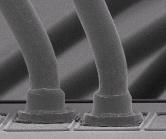
20 Kontaktování měděným drátkem Copper Wire Bond 20

21 Cu Wire Bond Proliferation: Advantages of Cu Wire bond becoming better known in industry, main driver is cost Migration from gold wire to cu wire for fine wire applications is moving quickly ASE conversion accounts for over 29% of total wire bond shipments, expected to reach >40% by end of
 Wire Bond Package (Cu Wire) Challenges : Surface Oxidation. Higher hardness. Al pad splash. Slow IMC growth. Cu Corrosion.")
22 Motivation: Significant cost benefit Expect 8% - 15% saving 100% Wire Cost Other Cost August 22 nd, 2011: 1,898$USD/ounce 50% 0% Wire Bond Package (Au Wire) Wire Bond Package (Cu Wire) Challenges : Surface Oxidation. Higher hardness. Al pad splash. Slow IMC growth. Cu Corrosion.

23 Cu Wire Bond Over three years in production 4+ billion units shipped: vast experience Multiples sites Taiwan, China, Korea, Japan, Malaysia Broad spectrum of market applications Cu wire bond at deep submicron nodes

24 Cu Wire Bond Technology Cu Wire Bonder sets installed by Q Aggressive ramp, culminating in 6700 sets by end of Q1 Q2 Q3 Q4 Q1 Q2 Q3 Q4

25 Cu Wire Bond Shipments Billion units More than 2 Billion units Billion units by the end of Estimates
26 Industry Migration by Package Cu wire bond shipments for QFNs 7.2% of 2010 unit shipments 19% of 2011 unit shipments Projected to be 78% in 2015 Cu wire bond shipments for PBGAs 4% of 2010 unit shipments 10% of 2011 unit shipments Projected to be 72% of unit shipments in 2015 Cu wire bond shipments for FBGAs 2.8% of 2010 unit shipments 8% of 2011 unit shipments Projected to be 36% of unit shipments by 2015 Cu wire bond shipments for stacked die CSPs Less than 1% of 2010 unit shipments 4.4% of 2011 unit shipments Projected to be 32% by 2015 Stacked die slowest application to transition, two-die stacks in early production, high number of die stacks remain in gold due to mechanical and material requirements of thin die Source: Techsearch International August
27 Cu Wire Bond Package Type 2009 Shipment by Volume 2010 Shipment by Volume 2010 Shipment by Revenue FBGA 7% PBGA 4% SOIC/ PLCC 14% TQFP 8% aqfn 0.3% QFN 16% LQFP 43% PQFP 8% PBGA 12% FBGA 18% SO/PLCC 7% TQFP 7% aqfn 1.5% LQFP 24% QFN 25% PQFP 6% BGA 47% SOIC/ PLCC 4% Discrete 1% QFN; 15% QFP 33%


28 Cu Wire Bond Wafer Technology 2010 Wafer Technology 2009 Wafer Technology 0.35um 10% 0.25um 5% >=0.4um 14% 65/60 nm 2% 90/80 nm 10% 0.13um 22% 0.25um 3% 0.35um 9% >= 0.4um 12% 40/45 nm 1% 60/65 nm 7% 0.13um 18% 90/80 nm 14% 0.18um 37% 0.18um 36%

29 Cu Wire Bond - Applications 2010 Applications 2009 Applications Auto 0.2% Communic ation 21% Power 10% Computing 15% Communication 24% Power 8% Computing 20% Consumer 54% Consumer 48%
30 Technology Roadmap Technology HVM Available Min wire Dia. 18(um) Die pad structure Tri-tiers/ Quadtiers Tri-tiers/ Quad-tiers Tri-tiers/ Quad-tiers Tri-tiers/ Quad-tiers Tri-tiers/ Quad-tiers Cu Wire Technology Min bond pad pitch Min bond pad opening Cu-LK wafer technology Bond pad surface Al Al 50(um) (um) /65(nm) 45/ Al / Au / Ni-Au / Ni-Pd / Ni-Pd-Au Al / Au / Ni-Au / Ni-Pd / Ni-Pd-Au Al / Au / Ni-Au / Ni-Pd / Ni-Pd-Au Low loop 75um 75um 55um 45um 45um Pad to pad Au+Cu Au+Cu Cu only Cu only Cu only
31 2010 Worldwide Copper Capacity Addition In 2010, ASE was the most aggressive in Cu bonder addition Cu Bonder Installation by Region 2010 IDM & SATS combined: 13K to 15K total Korea 1% Japan 3% Thailand 1% Europe 0% America 0% Others 2% Singapore 4% OSAT: ASE, SPIL IDMs: STM, FCS China 12% Taiwan 39% ASE SPIL Philippines 18% IDMs: TI, Renesas, FCS, On Semi Malaysia 20% OSAT: Carsem, Unisem IDMs: TI, Renesas, FCS Source: Kulicke & Soffa, Feb Gartner, Dec 2010.
32 3D integrace s mezivrstvovými propojkami (TSV, Through Silicon VIA) 32

33 3D SiPs to Meet Product Trends - Technology Integration, Form Factor & Performance QFP
34 3D IC TSV Package Development in ASE TSV in development since 2007 CIS TSV since 2008 (Via Last) Image Sensor Digital Signal Processor Si interposer since 2008 MEMS TSV in 2010 (Via Last) Memory stack on Logics since 2008 Heterogeneous chip integration in Memory Logic / CPU RF MEMS Memory Processor Si Interposer


35 Wafer Level Capabilities for 3D Via Formation Package Thin Wafer Handling um thick - 50 um under develop Double Side Photo- Litho - 15um/ 15um L/S qualified - 10um/10um L/S pro type - 2L metal layer - 20~100 um via - Aspect ratio 6~7 - Full-fill and lining available Microbump - 20um size/ 40um pitch - AR > Plating uniformity < 10% 40 um pitch Microbump


36 TSV Structure - with Polymer Isolation Isolation thickness up to 10 + um Good electrical performance & low leakage Good sidewall conformity & uniformity Low process temp. (<250ºC) Low via/ Si stress 12 um isolation/ 230um depth
 C2C/C2W Bonding Thermo-sonic bonding")
 Cu pillar/cu post (40um pitch)")

 50um chip-to-chip (under development) Encapsulation CUF")
 Cu pillar bump 80um/40um (under development)")
37 Major Process Challenges & Capabilities Micro bumps (C2C/C2W) Solder bump (100um) C2C/C2W Bonding Thermo-sonic bonding Thermo-compression bonding High precision FC bonding (3um) TSV-Via Last Au stud bump (50um pitch) Cu pillar/cu post (40um pitch) Micro solder bump (100um) Au stud Top chip Bottom chip 40um pitch Cu pillar F2F w/ wire bond Thin Wafer Handling 100um chip-to-substrate (qualified) 50um chip-to-substrate (Prototype available) 50um chip-to-chip (under development) Encapsulation CUF (< 15um gap) NCP NCF Wafer level dispenser (12 ) Bump pitch (chip-to-substrate) Cu pillar bump 80um/40um (under development) Solder bump 150um Au stud bump 60um 60um
38 Assembly Process Flow ASIC with RDL & Bump Wafer Saw Substrate Wafer Backside Grinding Si interposer die FC Si interposer Wafer saw ASIC die FC Underfill dispensing & cure Reflow oven Ball Mount & Singulation
39 2,5 D Si mezivložka 2.5D Si Interposer 2.5D IC Middle-end & Assembly
40 Si Interposer Benefits Alleviate ELK/ ULK stress in large die Bridge organic substrate gap for dense & complex substrate Package advanced wafer node w/ tighter bump pitch Integrate multi-chip SiP platform Match advanced wafer pitch Fan-out to match existing substrate capability Chip 1 Chip 2 Si Interposer Si - Si to minimize CTE impact on ELK


41 Si Interposer Enabling Chip Integration Alternative SoC Solution (Allow IC designer to partition chips and re-organize in Si interposer platform) Provide platform for heterogeneous chip integration (IPD, MEMS, Sensor ) +


42 Si Interposer Incorporate IPD solution Prototype : June 10 Capacitor Capacitance: 824 pf /mm 2 Range: pF Resistor Rs value: 85 ohm/sq Standard type: 12 10k ohm Inductor Inductance: 1~15nH Diplexer Balance Filter Band Pass Filter Balun
43 3D Si Mezivložka 3D Si Interposer 3D IC Middle-end & Assembly
44 Memory on ASIC Assembly Process Flow (D2S) Processor wafer 1. Processor Wafer (w/ Cu pillar bump) carrier 2. Mount processor wafer onto Carrier carrier 3. Middle-end Process carrier 4. Release Processor Wafer from Carrier 5. Processor Wafer Dicing 9. Marking, Ball Mount & Singulation Saw 8. Wafer Level Mold 7. Memory die TC Bonding to Processor * 6. Processor die TC Bonding to Substrate * ASE has developed a proprietary solution to control warpage
")
 C2S (H=50 um, Prototype) C2C (H=50 um,")
 Solder Bump (C2S) Cu Pillar Bump (Pitch=72um, Developing) Solder")
45 2.5D & 3D IC FC Assembly Capabilities C2C / C2W Bonding Micro Bumps (C2C / C2W) Thermo-sonic bonding Thermo-compression bonding High precision FC bonding (3um) Cu Pillar/Cu Post (Pitch=40um) Micro SnAg Solder Bump (Pitch=100um) Thin Wafer Handling C2S (H= 100 um, Ready) C2S (H=50 um, Prototype) C2C (H=50 um, Developing) Underfill CUF (< 15um Gap) Wafer Level Dispenser (8 ) MUF (Developing) Solder Bump (C2S) Cu Pillar Bump (Pitch=72um, Developing) Solder Bump (Pitch=150um)


46 2.5D & 3D IC FC Assembly Capabilities 50um thick bottom die 20um bump size/ 40um bump pitch 80um bump size/ 150um bump pitch


47 Concurrent Design on Electrical, Thermal & Mechanical Performance TSV RLC Modeling System Thermal Analysis 10% 9% Stress / Reliability Modeling Via R, L, C Modeling 81% Electro-Thermal Current Crowding Modeling Viscoplastic/ Creep Constitutive Model Darveaux/ Coffin-Manson Fatigue Model Validation Chip Substrate Maximum Stress Bump Crack Inter-delamination


48 Future 3D SiP Integration - Leverage building block portfolio (Ultimate SiP, System-in-a-Package) 3D TSV Embedded Actives Embedded Passives IPD EMI Shielding WLCSP Stacked Dies Advanced Materials (UF, MCP, Epoxy,..)
49 Děkuji za pozornost
3D Package Technologies Review with Gap Analysis for Mobile Application Requirements. Apr 22, 2014 STATS ChipPAC Japan
 3D Package Technologies Review with Gap Analysis for Mobile Application Requirements Apr 22, 2014 STATS ChipPAC Japan T.Nishio Contents Package trends and roadmap update Advanced technology update Fine
Challenges and Solutions for Cost Effective Next Generation Advanced Packaging. H.P. Wirtz, Ph.D. MiNaPAD Conference, Grenoble April 2012
 Challenges and Solutions for Cost Effective Next Generation Advanced Packaging H.P. Wirtz, Ph.D. MiNaPAD Conference, Grenoble April 2012 Outline Next Generation Package Requirements ewlb (Fan-Out Wafer
Nanium Overview. Company Presentation
 Nanium Overview Company Presentation Nanium Overview Our name and logo nano prefix of Greek origin referring to small objects ium suffix of Latin origin that includes the formation of scientific terms
System-in-Package (SiP) on Wafer Level, Enabled by Fan-Out WLP (ewlb)
 on Wafer Level, Enabled by Fan-Out WLP (ewlb)") System-in-Package (SiP) on Wafer Level, Enabled by Fan-Out WLP (ewlb) Steffen Kröhnert, José Campos, Eoin O Toole NANIUM S.A., Vila do Conde, Portugal Outline Short Company Overview NANIUM Introduction
System-in-Package (SiP) on Wafer Level, Enabled by Fan-Out WLP (ewlb) Steffen Kröhnert, José Campos, Eoin O Toole NANIUM S.A., Vila do Conde, Portugal Outline Short Company Overview NANIUM Introduction
Wire-Bond CABGA A New Near Die Size Packaging Innovation Yeonho Choi February 1, 2017
 Amkor Technology, Inc. White Paper Wire-Bond CABGA A New Near Die Size Packaging Innovation Yeonho Choi February 1, 2017 Abstract Expanding its ChipArray Ball Grid Array (CABGA) package form factor miniaturization
Outline. Market Size Industry Trends Material Segment Trends China Summary. Packaging Materials Market Trends, Issues and Opportunities
 Packaging Materials Market Trends, Issues and Opportunities Dan Tracy Sr. Director Industry Research SEMI 8 th December 2015 Outline Market Size Industry Trends Material Segment Trends China Summary 1
IME Technical Proposal. High Density FOWLP for Mobile Applications. 22 April High Density FOWLP Consortium Forum
 IME Technical Proposal High Density FOWLP for Mobile Applications 22 April 2014 Packaging driver for portable / mobile applications Key drivers/needs Smaller form-factor lower profile, substrate-less Higher
Cu Pillar Interconnect and Chip-Package-Interaction (CPI) for Advanced Cu Low K chip
 for Advanced Cu Low K chip") EPRC 12 Project Proposal Cu Pillar Interconnect and Chip-Package-Interaction (CPI) for Advanced Cu Low K chip 15 th Aug 2012 Page 1 Introduction: Motivation / Challenge Silicon device with ultra low k
EPRC 12 Project Proposal Cu Pillar Interconnect and Chip-Package-Interaction (CPI) for Advanced Cu Low K chip 15 th Aug 2012 Page 1 Introduction: Motivation / Challenge Silicon device with ultra low k
Hot Chips: Stacking Tutorial
 Hot Chips: Stacking Tutorial Choon Lee Technology HQ, Amkor Enabling a Microelectronic World Mobile Phone Technology Change Feature Phone Smartphone Smartphones as a Percentage of All Phones Source : The
Chips Face-up Panelization Approach For Fan-out Packaging
 Chips Face-up Panelization Approach For Fan-out Packaging Oct. 15, 2015 B. Rogers, D. Sanchez, C. Bishop, C. Sandstrom, C. Scanlan, TOlson T. REV A Background on FOWLP Fan-Out Wafer Level Packaging o Chips
Copper Wire Bonding: the Last Frontier of Cost Savings. Bernd K Appelt Business Development ASE (U.S.) Inc. April 11, 2012
 Inc. April 11, 2012") Copper Wire Bonding: the Last Frontier of Cost Savings Bernd K Appelt Business Development ASE (U.S.) Inc. April 11, 2012 Outline Introduction Fundamental Study Reliability Study Monitoring Data High Volume
Copper Wire Bonding: the Last Frontier of Cost Savings Bernd K Appelt Business Development ASE (U.S.) Inc. April 11, 2012 Outline Introduction Fundamental Study Reliability Study Monitoring Data High Volume
Semiconductor IC Packaging Technology Challenges: The Next Five Years
 SPAY025 May 2006 White Paper Mario A. Bolanos, Director Semiconductor Group Packaging Technology Development, Texas Instruments In the era of communications and entertainment, growth of consumer electronics
Panel Discussion: Advanced Packaging
 Dr. Steve Bezuk Senior Director IC Packaging Engineering Qualcomm Technologies, Inc. Panel Discussion: Advanced Packaging PAGE 1 Technical Challenges of Packaging (Mobile Focus) Materials Die materials
Semiconductor Packaging and Assembly 2002 Review and Outlook
 Gartner Dataquest Alert Semiconductor Packaging and Assembly 2002 Review and Outlook During 2002, the industry continued slow growth in unit volumes after bottoming out in September 2001. After a hearty
IMPLEMENTATION OF A FULLY MOLDED FAN-OUT PACKAGING TECHNOLOGY
 IMPLEMENTATION OF A FULLY MOLDED FAN-OUT PACKAGING TECHNOLOGY B. Rogers, C. Scanlan, and T. Olson Deca Technologies, Inc. Tempe, AZ USA boyd.rogers@decatechnologies.com ABSTRACT Fan-Out Wafer-Level Packaging
Close supply chain collaboration enables easy implementation of chip embedded power SiP
 Close supply chain collaboration enables easy implementation of chip embedded power SiP Gerald Weidinger, R&D Project Leader, AT&S AT & S Austria Technologie & Systemtechnik Aktiengesellschaft Fabriksgasse13
Thin Wafers Bonding & Processing
 Thin Wafers Bonding & Processing A market perspective 2012 Why New Handling Technologies Consumer electronics is today a big driver for smaller, higher performing & lower cost device configurations. These
RF System in Packages using Integrated Passive Devices
 RF System in Packages using Integrated Passive Devices by Kai Liu, YongTaek Lee, HyunTai Kim, Gwang Kim, and Billy Ahn STATS ChipPAC 1711 W. Greentree Drive, Suite #117, Tempe, AZ 85284, USA Tel: 480-222-1722
Cost effective 300mm Large Scale ewlb (embedded Wafer Level BGA) Technology
 Technology") Cost effective 300mm Large Scale ewlb (embedded Wafer Level BGA) Technology by Meenakshi Prashant, Seung Wook Yoon, Yaojian LIN and Pandi C. Marimuthu STATS ChipPAC Ltd. 5 Yishun Street 23, Singapore 768442
Cost effective 300mm Large Scale ewlb (embedded Wafer Level BGA) Technology by Meenakshi Prashant, Seung Wook Yoon, Yaojian LIN and Pandi C. Marimuthu STATS ChipPAC Ltd. 5 Yishun Street 23, Singapore 768442
Fan-out Wafer Level ewlb Technology as an Advanced System-in- Package Solution
 Fan-out Wafer Level ewlb Technology as an Advanced System-in- Package Solution by Jacinta Aman Lim and Vinayak Pandey, STATS ChipPAC, Inc. Aung Kyaw Oo, Andy Yong, STATS ChipPAC Pte. Ltd. Originally published
"ewlb Technology: Advanced Semiconductor Packaging Solutions"
 "ewlb Technology: Advanced Semiconductor Packaging Solutions" by Sharma Gaurav@, S.W. Yoon, Yap Yok Mian, Shanmugam Karthik, Yaojian Lin, Pandi C. Marimuthu and Yeong J. Lee* STATS ChipPAC Ltd. 5 Yishun
Innovative Integration Solutions for SiP Packages Using Fan-Out Wafer Level ewlb Technology
 Innovative Integration Solutions for SiP Packages Using Fan-Out Wafer Level ewlb Technology Jacinta Aman Lim, Vinayak Pandey* STATS ChipPAC Inc. 46429 Landing Parkway, Fremont, CA 94538, USA *STATS ChipPAC
TechARENA Packaging Exhibitor Session OCT/08, 2014 New WLP-Technology-Fusion Concept Steffen Kröhnert, Director of Technology, NANIUM S.A. V1.
 TechARENA Packaging Exhibitor Session OCT/08, 2014 New WLP-Technology-Fusion Concept Steffen Kröhnert, Director of Technology, NANIUM S.A. V1.0 EXT Notification NANIUM is highly committed to IP protection.
Challenges for Embedded Device Technologies for Package Level Integration
 Challenges for Embedded Device Technologies for Package Level Integration Kevin Cannon, Steve Riches Tribus-D Ltd Guangbin Dou, Andrew Holmes Imperial College London Embedded Die Technology IMAPS-UK/NMI
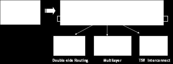
Innovative Substrate Technologies in the Era of IoTs
 Innovative Substrate Technologies in the Era of IoTs Dyi- Chung Hu 胡迪群 September 4, 2015 Unimicron Contents Introduction Substrate Technology - Evolution Substrate Technology - Revolution Glass substrate
IME Proprietary. EPRC 12 Project Proposal. 3D Embedded WLP. 15 th August 2012
 EPRC 12 Project Proposal 3D Embedded WLP 15 th August 2012 Motivation Factors driving IC market Higher density, lower cost, high yield Fan-out WLP/eWLP advantages Small footprint, low profile Low cost,
Advancements In Packaging Technology Driven By Global Market Return. M. G. Todd
 Advancements In Packaging Technology Driven By Global Market Return M. G. Todd Electronic Materials, Henkel Corporation, Irvine, California 92618, USA Recently, the focus of attention in the IC packaging
Mobile Device Passive Integration from Wafer Process
 Mobile Device Passive Integration from Wafer Process Kai Liu, YongTaek Lee, HyunTai Kim, and MaPhooPwint Hlaing STATS ChipPAC, Inc. 1711 West Greentree, Suite 117, Tempe, Arizona 85284, USA Tel: 48-222-17
3D-WLCSP Package Technology: Processing and Reliability Characterization
 3D-WLCSP Package Technology: Processing and Reliability Characterization, Paul N. Houston, Brian Lewis, Fei Xie, Ph.D., Zhaozhi Li, Ph.D.* ENGENT Inc. * Auburn University ENGENT, Inc. 2012 1 Outline Packaging
FOR SEMICONDUCTORS 2007 EDITION
 INTERNATIONAL TECHNOLOGY ROADMAP FOR SEMICONDUCTORS 2007 EDITION ASSEMBLY AND PACKAGING THE ITRS IS DEVISED AND INTENDED FOR TECHNOLOGY ASSESSMENT ONLY AND IS WITHOUT REGARD TO ANY COMMERCIAL CONSIDERATIONS
Recent Trends of Package Warpage and Measurement Metrologies (inemi Warpage Characterization Project Phase 3)
") Recent Trends of Package Warpage and Measurement Metrologies (inemi Warpage Characterization Project Phase 3) Wei Keat Loh 1, Ron Kulterman 2, Haley Fu 3, Masahiro Tsuriya 3 1 Intel Technology Sdn. Bhd.
Recent Trends of Package Warpage and Measurement Metrologies (inemi Warpage Characterization Project Phase 3) Wei Keat Loh 1, Ron Kulterman 2, Haley Fu 3, Masahiro Tsuriya 3 1 Intel Technology Sdn. Bhd.
Design and Assembly Process Implementation of 3D Components
 IPC-7091 Design and Assembly Process Implementation of 3D Components Developed by the 3-D Electronic Packages Subcommittee (B-11) of the Packaged Electronic Components Committee (B-10) of IPC Users of
Board Level Reliability Improvement in ewlb (Embedded Wafer Level BGA) Packages
 Packages") Board Level Reliability Improvement in ewlb (Embedded Wafer Level BGA) Packages by Seng Guan Chow, Yaojian Lin, Bernard Adams * and Seung Wook Yoon** STATS ChipPAC Ltd. 5 Yishun Street 23, Singapore 768442
Board Level Reliability Improvement in ewlb (Embedded Wafer Level BGA) Packages by Seng Guan Chow, Yaojian Lin, Bernard Adams * and Seung Wook Yoon** STATS ChipPAC Ltd. 5 Yishun Street 23, Singapore 768442
Novel Materials and Activities for Next Generation Package. Hitachi Chemical., Co.Ltd. Packaging Solution Center Hiroaki Miyajima
 Novel Materials and Activities for Next Generation Package Hitachi Chemical., Co.Ltd. Packaging Solution Center Hiroaki Miyajima 1. Activities of Packaging Solution Center 2. Novel Materials for Next Gen.
TSV CHIP STACKING MEETS PRODUCTIVITY
 TSV CHIP STACKING MEETS PRODUCTIVITY EUROPEAN 3D TSV SUMMIT 22-23.1.2013 GRENOBLE HANNES KOSTNER DIRECTOR R&D BESI AUSTRIA OVERVIEW Flip Chip Packaging Evolution The Simple World of C4 New Flip Chip Demands
An Innovative High Throughput Thermal Compression Bonding Process
 An Innovative High Throughput Thermal Compression Bonding Process Li Ming 2 September 2015 Outline Introduction Throughput improved TCB Process Liquid Phase Contact (LPC) bonding Flux-LPC-TCB under inert
Fanout Flipchip ewlb (embedded Wafer Level Ball Grid Array) Technology as 2.5D Packaging Solution
 Technology as 2.5D Packaging Solution") Fanout Flipchip ewlb (embedded Wafer Level Ball Grid Array) Technology as 2.5D Packaging Solution by Seung Wook Yoon,*Patrick Tang, **Roger Emigh, Yaojian Lin, Pandi C. Marimuthu, and *Raj Pendse STATS
Fanout Flipchip ewlb (embedded Wafer Level Ball Grid Array) Technology as 2.5D Packaging Solution by Seung Wook Yoon,*Patrick Tang, **Roger Emigh, Yaojian Lin, Pandi C. Marimuthu, and *Raj Pendse STATS
System in Package: Identified Technology Needs from the 2004 inemi Roadmap
 System in Package: Identified Technology Needs from the 2004 inemi Roadmap James Mark Bird Amkor Technology Inc System in package (SiP) technology has grown significantly in the past several years. It
Copyright 2009 Year IEEE. Reprinted from 2009 Electronic Components and Technology Conference. Such permission of the IEEE does not in any way imply
 Copyright 2009 Year IEEE. Reprinted from 2009 Electronic Components and Technology Conference. Such permission of the IEEE does not in any way imply IEEE endorsement of any of Institute of Microelectronics
3D Integrated ewlb /FO-WLP Technology for PoP & SiP
 3D Integrated ewlb /FO-WLP Technology for PoP & SiP by Yaojian Lin, Chen Kang, Linda Chua, Won Kyung Choi and *Seung Wook Yoon STATS ChipPAC Pte Ltd. 5 Yishun Street 23, Singapore 768442 *STATS ChipPAC
Advanced Analytical Techniques for Semiconductor Assembly Materials and Processes. Jason Chou and Sze Pei Lim Indium Corporation
 Advanced Analytical Techniques for Semiconductor Assembly Materials and Processes Jason Chou and Sze Pei Lim Indium Corporation Agenda Company introduction Semiconductor assembly roadmap challenges Fine
FRAUNHOFER INSTITUTE FOR RELIABILITY AND MICROINTEGRATION IZM DEPARTMENT WAFER LEVEL SYSTEM INTEGRATION BERLIN
 FRAUNHOFER INSTITUTE FOR RELIABILITY AND MICROINTEGRATION IZM DEPARTMENT WAFER LEVEL SYSTEM INTEGRATION BERLIN WAFER LEVEL SYSTEM INTEGRATION ELECTRONIC PACKAGING AT FRAUNHOFER IZM The Fraunhofer Institute
Development of Next-Generation ewlb Packaging
 Development of Next-Generation ewlb Packaging by Seung Wook Yoon, Yaojian Lin, Pandi Chelvam Marimuthu and *Rajendra Pendse STATS ChipPAC Singapore *Fremont, California USA Ganesh V. P, Andreas Bahr and
II. A. Basic Concept of Package.
 Wafer Level Package for Image Sensor Module Won Kyu Jeung, Chang Hyun Lim, Jingli Yuan, Seung Wook Park Samsung Electro-Mechanics Co., LTD 314, Maetan3-Dong, Yeongtong-Gu, Suwon, Gyunggi-Do, Korea 440-743
Package Solutions and Innovations
 Package Solutions and Innovations with Compression Molding IEEE SVC CPMT Aug 2015 Presented by C.H. Ang Towa USA Company Profile www.cpmt.org/scv 1 Corporate Overview Company: Towa Corp., Kyoto Japan Established:
TSV Processing and Wafer Stacking. Kathy Cook and Maggie Zoberbier, 3D Business Development
 TSV Processing and Wafer Stacking Kathy Cook and Maggie Zoberbier, 3D Business Development Outline Why 3D Integration? TSV Process Variations Lithography Process Results Stacking Technology Wafer Bonding
Recent Advances in Die Attach Film
 Recent Advances in Die Attach Film Frederick Lo, Maurice Leblon, Richard Amigh, and Kevin Chung. AI Technology, Inc. 70 Washington Road, Princeton Junction, NJ 08550 www.aitechnology.com Abstract: The
Failure Modes in Wire bonded and Flip Chip Packages
 Failure Modes in Wire bonded and Flip Chip Packages Mumtaz Y. Bora Peregrine Semiconductor San Diego, Ca. 92121 mbora@psemi.com Abstract The growth of portable and wireless products is driving the miniaturization
Thales vision & needs in advanced packaging for high end applications
 Thales vision & needs in advanced packaging for high end applications M. Brizoux, A. Lecavelier Thales Global Services / Group Industry Chemnitzer Seminar June 23 th -24 th, 2015 Fraunhofer ENAS - Packaging
Ultra Fine Pitch Bumping Using e-ni/au and Sn Lift-Off Processes
 Ultra Fine Pitch Bumping Using e-ni/au and Sn Lift-Off Processes Andrew Strandjord, Thorsten Teutsch, and Jing Li Pac Tech USA Packaging Technologies, Inc. Santa Clara, CA USA 95050 Thomas Oppert, and
SEMI MEMS Tech Seminar (Sept 26, Cornaredo, Italy)
") SEMI MEMS Tech Seminar (Sept 26, 2013 - Cornaredo, Italy) Opportunities of Wafer Level Embedded Technologies for MEMS Devices T. Braun ( 1 ), K.-F. Becker ( 1 ), R. Kahle ( 2 ), V. Bader ( 1 ), S. Voges
SEMI MEMS Tech Seminar (Sept 26, 2013 - Cornaredo, Italy) Opportunities of Wafer Level Embedded Technologies for MEMS Devices T. Braun ( 1 ), K.-F. Becker ( 1 ), R. Kahle ( 2 ), V. Bader ( 1 ), S. Voges
Chip Packaging for Wearables Choosing the Lowest Cost Package
 Chip Packaging for Wearables Choosing the Lowest Cost Package Alan Palesko alanp@savansys.com (512) 402-9943 www.savansys.com Slide - 1 Agenda Introduction Wearable Requirements Packaging Technologies
Next Generation ewlb (embedded Wafer Level BGA) Packaging
 Packaging") Next Generation ewlb (embedded Wafer Level BGA) Packaging by Meenakshi Prashant, Kai Liu, Seung Wook Yoon Yonggang Jin, Xavier Baraton, S. W. Yoon*, Yaojian Lin*, Pandi C. Marimuthu*, V. P. Ganesh**, Thorsten
Next Generation ewlb (embedded Wafer Level BGA) Packaging by Meenakshi Prashant, Kai Liu, Seung Wook Yoon Yonggang Jin, Xavier Baraton, S. W. Yoon*, Yaojian Lin*, Pandi C. Marimuthu*, V. P. Ganesh**, Thorsten
TSV Interposer Process Flow with IME 300mm Facilities
 TSV Interposer Process Flow with IME 300mm Facilities Property of Institute of Microelectronics (IME)-Singapore August 17, 2012 Outline 1. TSV interposer (TSI) cross sectional schematic TSI with BEOL,
Forschung für die Elektroniksysteme von morgen
 Forschung für die Elektroniksysteme von morgen R. Aschenbrenner Outline Trends in Advanced Packaging Was ist Panel Level Packaging Embedding für Fan Out Embedding für LP Beispiele Trend on ICs and Packages
Silicon Interposers with Integrated Passive Devices: Ultra-Miniaturized Solution using 2.5D Packaging Platform
 Minapad 2014, May 21 22th, Grenoble; France Silicon Interposers with Integrated Passive Devices: Ultra-Miniaturized Solution using 2.5D Packaging Platform Stéphane Bellenger, Laëtitia Omnès, Jean-René
3D & 2½D Test Challenges Getting to Known Good Die & Known Good Stack
 1 3D & 2½D Test Challenges Getting to Known Good Die & Known Good Stack Advantest Corporation 2 The final yield Any Multi-die Product Must Consider the Accumulated Yield Assume Test Can Provide 99% Die
Thermo-Mechanical Reliability of Through-Silicon Vias (TSVs)
") 1 Thermo-Mechanical Reliability of Through-Silicon Vias (TSVs) Xi Liu Ph.D. Student and Suresh K. Sitaraman, Ph.D. Professor The George W. Woodruff School of Mechanical Engineering Georgia Institute of
1 Thermo-Mechanical Reliability of Through-Silicon Vias (TSVs) Xi Liu Ph.D. Student and Suresh K. Sitaraman, Ph.D. Professor The George W. Woodruff School of Mechanical Engineering Georgia Institute of
2.5D and 3D Semiconductor Package Technology: Evolution and Innovation
 2.5D and 3D Semiconductor Package Technology: Evolution and Innovation Vern Solberg Solberg Technical Consulting Saratoga, California USA Abstract The electronics industry is experiencing a renaissance
Basic PCB Level Assembly Process Methodology for 3D Package-on-Package
 Basic PCB Level Assembly Process Methodology for 3D Package-on-Package Vern Solberg STC-Madison Madison, Wisconsin USA Abstract The motivation for developing higher density IC packaging continues to be
Bridging Supply Chain Gap for Exempt High-Reliability OEM s
 Bridging Supply Chain Gap for Exempt High-Reliability OEM s Hal Rotchadl hrotchadl@premiers2.com www.premiers2.com Premier Semiconductor Services Tempe, AZ RoHS exempt high reliability OEMs breathed a
Test Flow for Advanced Packages (2.5D/SLIM/3D)
") 1 Test Flow for Advanced Packages (2.5D/SLIM/3D) Gerard John Amkor Technology Inc. Gerard.John@amkor.com 2045 East Innovation Circle, Tempe, AZ 85284, USA Phone: (480) 821-5000 ADVANCED PACKAGE TEST FLOW
1 Test Flow for Advanced Packages (2.5D/SLIM/3D) Gerard John Amkor Technology Inc. Gerard.John@amkor.com 2045 East Innovation Circle, Tempe, AZ 85284, USA Phone: (480) 821-5000 ADVANCED PACKAGE TEST FLOW
Ultralow Residue Semiconductor Grade Fluxes for Copper Pillar Flip-Chip
 Ultralow Residue Semiconductor Grade Fluxes for Copper Pillar Flip-Chip SzePei Lim (Presenter), Jason Chou, Maria Durham, and Dr. Andy Mackie Indium Corporation 1 Outline of Presentation Roadmaps and challenges
The 3D Silicon Leader
 The 3D Silicon Leader TSV technology embedding high density capacitors for advanced 3D packaging solutions IMAPS Device Packaging Conference 2014 Catherine Bunel 2014.03.12 Outline Introduction IPDiA s
Alternative Approaches to 3-Dimensional Packaging and Interconnection
 Alternative Approaches to 3-Dimensional Packaging and Interconnection Joseph Fjelstad SiliconPipe, Inc. www.sipipe.com IC Packaging a Technology in Transition In the past, IC packaging has been considered
White Paper Quality and Reliability Challenges for Package on Package. By Craig Hillman and Randy Kong
 White Paper Quality and Reliability Challenges for Package on Package By Craig Hillman and Randy Kong Background Semiconductor technology advances have been fulfilling Moore s law for many decades. However,
Die Attach Materials. Die Attach G, TECH. 2U. TECHNICAL R&D DIV.
 Die Attach Materials Die Attach G, TECH. 2U. TECHNICAL R&D DIV. 2 Topics 3 What it is X 5,000 X 10,000 X 50,000 Si Chip Au Plating Substrate Ag Resin 4 Current Products Characteristics H9890-6A H9890-6S
Roundtable 3DIC & TSV: Ready for HVM? European 3D TSV Summit
 Roundtable 3DIC & TSV: Ready for HVM? European 3D TSV Summit Infineon VTI Xilinx Synopsys Micron CEA LETI 2013 Yann Guillou Business Development Manager Lionel Cadix Market & Technology Analyst, Advanced
Innovative Advanced Wafer Level Packaging with Smart Manufacturing Solutions YOON Seung Wook, Ph.D MBA
 Innovative Advanced Wafer Level Packaging with Smart Manufacturing Solutions YOON Seung Wook, Ph.D MBA Director, STATS ChipPAC Outline 1 2 3 Introduction of Smart Manufacturing & Wafer Level Packaging
FABRICATION AND RELIABILITY OF ULTRA-FINE RDL STRUCTURES IN ADVANCED PACKAGING BY EXCIMER LASER ABLATION
 FABRICATION AND RELIABILITY OF ULTRA-FINE RDL STRUCTURES IN ADVANCED PACKAGING BY EXCIMER LASER ABLATION NCCAVS Joint Users Group Technical Symposium San Jose, June 7 th, 2017 Markus Arendt, SÜSS MicroTec
Warpage Mechanism of Thin Embedded LSI Packages
 Nakashima et al.: Warpage Mechanism of Thin Embedded LSI Packages (1/10) [Technical Paper] Warpage Mechanism of Thin Embedded LSI Packages Yoshiki Nakashima*, Katsumi Kikuchi*, Kentaro Mori*, Daisuke Ohshima**,
Avatrel Stress Buffer Coatings: Low Stress Passivation and Redistribution Applications
 Avatrel Stress Buffer Coatings: Low Stress Passivation and Redistribution Applications Ed Elce, Chris Apanius, Jeff Krotine, Jim Sperk, Andrew Bell, Rob Shick* Sue Bidstrup-Allen, Paul Kohl Takashi Hirano,
TGV and Integrated Electronics
 TGV and Integrated Electronics Shin Takahashi ASAHI GLASS CO., LTD. 1 Ambient Intelligence Green Energy/Environment Smart Factory Smart Mobility Smart Mobile Devices Bio/Medical Security/Biometrics 2 Glass
Design for Flip-Chip and Chip-Size Package Technology
 Design for Flip-Chip and Chip-Size Package Technology Vern Solberg Solberg Technology Consulting Madison, Wisconsin Abstract As new generations of electronic products emerge they often surpass the capability
3D Wirebondless IGBT Module for High Power Applications Dr. Ziyang GAO Jun. 20, 2014
 3D Wirebondless IGBT Module for High Power Applications Dr. Ziyang GAO Jun. 20, 2014 1 1 Outline Background Information Technology Development Trend Technical Challenges ASTRI s Solutions Concluding Remarks
YOUR Strategic TESTING ENGINEERING CONCEPT SMT FLIP CHIP PRODUCTION OPTO PACKAGING PROCESS DEVELOPMENT CHIP ON BOARD SUPPLY CHAIN MANAGEMENT
 YOUR Strategic TECHNOLOGY PARTNER Wafer Back-End OPTO PACKAGING PROCESS DEVELOPMENT CONCEPT FLIP CHIP PROTOTYping ENGINEERING TESTING SMT PRODUCTION CHIP ON BOARD SUPPLY CHAIN MANAGEMENT Next Level 0f
Silicon Wafer Processing PAKAGING AND TEST
 Silicon Wafer Processing PAKAGING AND TEST Parametrical test using test structures regularly distributed in the wafer Wafer die test marking defective dies dies separation die fixing (not marked as defective)
Graser User Conference Only
 2.5D/3D Design Solution Eric Chen & Scott Liu 31/Oct/2014 Roadmap data is provided for informational purposes only and does not represent a commitment to deliver any of the features or functionality discussed
Wafer Level Packaging
 1 IEEE CPMT Meeting, San Jose, CA Wafer Level Packaging L. Nguyen National Semiconductor Corp. Santa Clara, CA Acknowledgments: N. Kelkar, V. Patwardhan, C. Quentin, H. Nguyen, A. Negasi, E. Warner Feb-02
Development of System in Package
 Development of System in Package In recent years, there has been a demand to offer increasingly enhanced performance for a SiP that implements downsized and lower-profile chips at lower cost. This article
Power Electronics Packaging Solutions for Device Junction Temperature over 220 o C
 EPRC 12 Project Proposal Power Electronics Packaging Solutions for Device Junction Temperature over 220 o C 15 th August 2012 Page 1 Motivation Increased requirements of high power semiconductor device
Development of Exposed Die Large Body to Die Size Ratio Wafer Level Package Technology
 Development of Exposed Die Large Body to Die Size Ratio Wafer Level Package Technology by J. Osenbach 1, S. Emerich1, L. Golick1, S. Cate 2, M. Chan3, S.W. Yoon 3, Y.J. Lin 4 & K. Wong 5, 1LSI Corporation
28nm Mobile SoC Copper Pillar Probing Study. Jose Horas (Intel Mobile Communications) Amy Leong (MicroProbe) Darko Hulic (Nikad)
 Amy Leong (MicroProbe) Darko Hulic (Nikad)") 28nm Mobile SoC Copper Pillar Probing Study Jose Horas (Intel Mobile Communications) Amy Leong (MicroProbe) Darko Hulic (Nikad) Overview Introduction to IMC Copper Pillar Implementation at IMC Low force
28nm Mobile SoC Copper Pillar Probing Study Jose Horas (Intel Mobile Communications) Amy Leong (MicroProbe) Darko Hulic (Nikad) Overview Introduction to IMC Copper Pillar Implementation at IMC Low force
Selection and Application of Board Level Underfill Materials
 Selection and Application of Board Level Underfill Materials Developed by the Underfill Materials Design, Selection and Process Task Group (5-24f) of the Assembly and Joining Committee (5-20) of IPC Supersedes:
Copper Wire Packaging Reliability for Automotive and High Voltage
 Copper Wire Packaging Reliability for Automotive and High Voltage Tu Anh Tran AMPG Package Technology Manager Aug.11.2015 TM External Use Agenda New Automotive Environments Wire Bond Interconnect Selection
Bonding Wires for Semiconductor Technology
 Bonding Wires for Semiconductor Technology Contents History 4 Superior Bonding Wire Technology 5 Research & Development 6 Bonding Wire Technology Laboratory & Applications 7 Commitment to Product and Service
Flip Chip - Integrated In A Standard SMT Process
 Flip Chip - Integrated In A Standard SMT Process By Wilhelm Prinz von Hessen, Universal Instruments Corporation, Binghamton, NY This paper reviews the implementation of a flip chip product in a typical
Flexible Carrier Enables Automated Test-in-Tray. Dr. Tom Di Stefano Centipede Systems
 Flexible Carrier Enables Automated Test-in-Tray Dr. Tom Di Stefano Centipede Systems Running in Parallel TnT is limited only by Test Electronics Parallel test at fixed DUT positions Parallel to 256+ DUTS
Development of Multi Chip Modules for Extreme Environments. Hyun Joong Lee
 Development of Multi Chip Modules for Extreme Environments by Hyun Joong Lee A thesis submitted to the Graduate Faculty of Auburn University in partial fulfillment of the requirements for the Degree of
FLIP CHIP CHIP ON BOARD SMT ENGINEERING OPTO PACKAGING SUPPLY CHAIN MANAGEMENT TESTING YOUR INNOVATIVE TECHNOLOGY PARTNER PRODUCTION CONCEPT
 YOUR INNOVATIVE TECHNOLOGY PARTNER CHIP ON BOARD OPTO PACKAGING PROCESS DEVELOPMENT CONCEPT FLIP CHIP ENGINEERING TESTING PRODUCTION SMT SUPPLY CHAIN MANAGEMENT PROTOTYPES HIGH-PRECISION ASSEMBLY OF MICRO-
Effectiveness of Conformal Coat to Prevent Corrosion of Nickel-palladium-goldfinished
 As originally published in the IPC APEX EXPO Conference Proceedings. Effectiveness of Conformal Coat to Prevent Corrosion of Nickel-palladium-goldfinished Terminals Michael Osterman Center for Advanced
Low Temperature Co-fired Ceramics (LTCC) Multi-layer Module Boards
 Multi-layer Module Boards") Low Temperature Co-fired Ceramics () Multi-layer Module Boards Example: Automotive Application Example: Communication Application Murata's Low Temperature Co-fired Ceramics offer highly integrated substrates
Low Temperature Co-fired Ceramics () Multi-layer Module Boards Example: Automotive Application Example: Communication Application Murata's Low Temperature Co-fired Ceramics offer highly integrated substrates
A New Company & Approach In MEMS Semiconductor Materials & Engineering Services
 A New Company & Approach In MEMS Semiconductor Materials & Engineering Services www.ubotic.com Semi Networking Day Italy Founded & Location Founded in 2009 Hong Kong & Dongguan, China Company Background
23 rd ASEMEP National Technical Symposium
 THE EFFECT OF GLUE BOND LINE THICKNESS (BLT) AND FILLET HEIGHT ON INTERFACE DELAMINATION Raymund Y. Agustin Janet M. Jucar Jefferson S. Talledo Corporate Packaging & Automation/ Q&R STMicroelectronics,
High Density PoP (Package-on-Package) and Package Stacking Development
 and Package Stacking Development") High Density PoP (Package-on-Package) and Package Stacking Development Moody Dreiza, Akito Yoshida, *Kazuo Ishibashi, **Tadashi Maeda, Amkor Technology Inc. 1900 South Price Road, Chandler, AZ 85248, U.S.A.
High Density PoP (Package-on-Package) and Package Stacking Development Moody Dreiza, Akito Yoshida, *Kazuo Ishibashi, **Tadashi Maeda, Amkor Technology Inc. 1900 South Price Road, Chandler, AZ 85248, U.S.A.
Embedded Cooling Solutions for 3D Packaging
 IME roprietary ERC 12 roject roposal Embedded Cooling Solutions for 3D ackaging 15 th August 2012 age 1 Technology & ower Dissipation Trends IME roprietary Cannot continue based on Moore s law scaling
New Technology for High-Density LSI Mounting in Consumer Products
 New Technology for High-Density Mounting in Consumer Products V Hidehiko Kira V Akira Takashima V Yukio Ozaki (Manuscript received May 29, 2006) The ongoing trend toward downsizing and the growing sophistication
Encapsulation Selection, Characterization and Reliability for Fine Pitch BGA (fpbga )
") Encapsulation Selection, Characterization and Reliability for Fine Pitch BGA (fpbga ) Henry M.W. Sze, Marc Papageorge ASAT Limited 14th Floor, QPL Industrial Building, 138 Texaco Road, Tseun Wan, Hong
Encapsulation Selection, Characterization and Reliability for Fine Pitch BGA (fpbga ) Henry M.W. Sze, Marc Papageorge ASAT Limited 14th Floor, QPL Industrial Building, 138 Texaco Road, Tseun Wan, Hong
Analog Devices ADSP KS-160 SHARC Digital Signal Processor
 Construction Analysis Analog Devices ADSP-21062-KS-160 SHARC Digital Signal Processor Report Number: SCA 9712-575 Global Semiconductor Industry the Serving Since 1964 17350 N. Hartford Drive Scottsdale,