Design For Probe: Probe Card Selection Process
|
|
|
- Alicia Dorsey
- 5 years ago
- Views:
Transcription


1 Design For Probe: Probe Card Selection Process Brandon Mair Dawn Copeland 6/10/2014
2 Agenda DFP Overview TI Qualified Vendors Qualification Process Probe Technologies Specifications / Documentation Benefits of DFP Process Questions / Discussion B. Mair and D. Copeland 2


3 Design For Probe Overview DFP Design For Probe is a risk review process involving a cross functional team of experienced probe test members whose objective is to target probe solutions that are aligned to TI's Roadmap and Best Practices. Probe Card Tech ISMI External Benchmarks Tester Dev Wafer Probe Solution Prober Mech Interface WPL/PCB Benefits Optimize the Probe Card technology selection! Build the right Probe Card for your device. Take advantage of the latest qualifications Understand each test floor s strengths for smooth offload. Maintain Probe Card Build Spec Monitor vendor compliance to avoid probe card mis builds and lost cycle time WPL assists with RFQ to ensure best pricing! Design Rules for various silicon technologies. Help to provide robust solutions that can easily be transferred across various TI sites worldwide. LBE Die /Test Req ds Adv Package Req ds Ex: Cantilever design rules below for pad layout. Test Flr Operations Infra-HW B. Mair and D. Copeland 3


4 Design For Probe Organization Brandon Mair DFP Team Lead Test Sites Probe Test Solutions Business Units B. Mair and D. Copeland 4
5 Design for Probe Process Flow Approved PC Vendor List TI Probe Roadmap Additional CTFs, COO, RFQ DEVICE LIST Probe Feature Surface Type Minimum Probe Pitch (microns) Test Feature Pattern on Die Test Application (RF/NRF/NRF-Kelvin) Total Number of Probes per Die Multi- Site Number Total Number of Probes / TD? Maximum Signal Frequency? (MHz) CCC- Current Carrying Capability (ma) Probe Test Temperature? ( C) Probe Test Temperature? C) Business Unit (SBE) Business Unit (LBE) Program Mgr Test Engr CMOS / Analog Technology Probe Feature Surface Metallurgy Minimum Probe Pad/Bump Size Separate Probe / Bond areas? (Y/N) Probing on Bond area? (Y/N) Mixed Pad Dimensions? (Y/N) PC Selection Tool Vendor A, B,.? DFP Review Selected PC Vendor/ Tech Roadmap Development Device Test Modification The Design for Probe Team utilizes the Business Unit s device input to determine the best probe card technology and vendor. The recommendations are based on cost of ownership models for pricing and lifetime performance. B. Mair and D. Copeland 5


6 Device Input for the Selection Process Device Input list requests relevant information about the device. All parameters are input into the Probe Card Selection Tool to select qualified probe card vendors and technologies. B. Mair and D. Copeland 6

7 DFP Device Spreadsheet Data Sample from Device List. Collecting different data from each device to allow for easy tracking / review of data. B. Mair and D. Copeland 7
8 Probe Card Selection Tool: Objective: In the past, DFP has relied on manual inputs and tribal knowledge of DFP members or TI test community to select an appropriate probe card technology and vendor. As a result, the Probe Card Selection Tool was developed to automate / capture the probe CTFs critical to function parameters, to make better and more consistent decisions in a timely and cost effective manner for TI WW. PTS used third party software from Logicnets to aid in automation of the probe card technology decision process in a systematic manner. B. Mair and D. Copeland 8
9 Probe Card Selection Tool The first set of screens ask for the basic parameters to identify and track the device being processed. B. Mair and D. Copeland 9


10 Probe Card Selection Tool: Required Inputs Core Pads 50 um B. Mair and D. Copeland 10
11 Probe Card Selection Tool: Supplemental Device Inputs Supplemental information helps to further narrow down vendor / technology decision. B. Mair and D. Copeland 11
12 Probe Card Selection Tool: Input and Output Input: EXAMPLE Device Output: 2 Qualified PC Vendors / technologies. WPL Submits RFQ for LBE review and selection. Output: Vendor Technology Technology Name Vendor Contact Vendor Vendor Website Superman Inc Vertical Kryptonite Clark Kent clarkkent@superman.com Batman Technologies Vertical Crusader Bruce Wayne bwayne@batman.com B. Mair and D. Copeland 12

13 2013 DFP Results Breakout of which groups are using DFP and how many devices they had this year. Devices run through DFP this year 66% Pad devices 33% Bump devices B. Mair and D. Copeland 13
14 WPL Quoting Process WPL helps to provide cost analysis between available technologies for each device. Rebuild cost is also a factor considered when comparing the various vendors. B. Mair and D. Copeland 14


15 Stepping Efficiency Tool can go through multiple designs in a matter of minutes to find most optimal design based upon wafer layout. Stepping Efficiency Tool can help to quickly determine most optimal stepping efficiency pattern as well as stepping pattern across the wafer. B. Mair and D. Copeland 15

16 Current Modeling Tool Developed a tool to help provide guidelines on which technologies / vendors can handle device required current. Tool available to use in DFP process so that we can make sure technology chosen can handle required current. B. Mair and D. Copeland 16
17 TI Qualified Vendors B. Mair and D. Copeland 17
18 TI Qualified Vendors For each vendor used, an extensive qualification process is used to ensure that the vendor / technology performs up to standard mechanically and electrically over time. Part of this qualification is also a cleaning evaluation to ensure that cleaning procedures / cleaning media are optimal. B. Mair and D. Copeland 18
19 Qualification Process Technology Production QUALIFICATION PASSES Category PASSES Category DOES NOT QUALIFY DOES NOT QUALIFY Meets required CTF Critical To Function parameters. Passes qualification category for the particular probe requirements envelope or node intended. e.g. 70 um, x32/x64 multi site enablement Meets most CTF Critical To Function parameters. Passes qualification step. However, contingent on additional data, data analysis either on line or off line to resolve. Does not meet most CTF critical to function parameters. Does not pass qualification category. Not considered a show stopper; however, ARs required to be resolved Does not meet required CTF critical to function parameters. Does not pass qualification category. Considered a show stopper, significant work required to resolve. TECH QUAL PROD QUAL INTEGRATION B. Mair and D. Copeland 19
20 Qualification Worksheet bin to bin correlation Dielectric cracking Punch through Cres over time Test Cleaning rotation as it relates to Cres and contact related bin fails New material has a requirement of a MSDS, no polyethylene allowed, high temp transfer study is needed Requirement 98% bin to bin from baseline card to new probe technology or LBE/PDE acceptance Dielectric cracking study Automotive requirement 9x TD in the same location and max production probing OT) No under layer metal exposure on automotive products QSS states for Al technologies shall not expose underlying passivation or underlying metal equal to or greater than 25% of the pad width adjacent to the edge of the pad or exceeds 1.0mil2 near the center of the bond pad. 3 Ohms Standard deviation 100k TD and a minimum 100 wafers Probed How many rotations of the cleaning material? 100k TD and a minimum 100 wafers Probed in production or accelerated probing and cleaning wear study to show the TD vs. Tip length as it relates to probe card end of life. (life expected must be Life time study (>750K TD) Prober device file set up needle tip alignment settings Total Qual X X X X X Cleaning Qual Results Data Pass/Fail X X 94% bin to bin correlation approved by the LBE Yvonne So Bin2Bin Pass No dielectric cracking report needed for Bump Material No punch through report need for bump material Cleaning Media 1um Grit ProbeLapp Cleaning Settign 25 wafer TD 10 Cres across 9k dies 0.15Ω Stdev Cres Data Pass Cleaning Media 1um Grit ProbeLapp Cleaning Settign 25 wafer TD 10 Cres across 9k dies 0.15Ω Stdev Cres Data Pass X X ProbeLap is currently used in production at C MSDS Pass X X X Card Life Data shows TD production probing Needle tip Algorithm 0 Standard size Life Time Data NA NA Pass Pass PHYSICAL DESIGN PROCESS MANUFACTURING SUSTAINABILITY TEST PERFORMANCE RELIABILITY TEST OPERATIONS FUTURE APPLICABLITY COST OF OWNERSHIP OVERALL ASSESSMENT AVI fail rate Bump Damage Thermal agility fail rate must be less the 0.25% across 20 EWR lots at all temperatures. Damage must meet all packaging requirments X, Y, Z correction across a wafer must be lest the 30um min to max without dramatic swings not including stops to the prober with in a wafer once the card gets to temps X X X No AVI data for Bump probing Mushroom probing showed no damage Reflow bumps require packaging sample eval YIELD: FT % PB % PB % Bump devices do not probe at high temp no optical alignment data needed Bump Damage NA Pass NA B. Mair and D. Copeland 20
21 Probe Card Technology B. Mair and D. Copeland 21
22 Probe Card Technologies Categories vs. TI Device Node/Test Feature Probe Requirements RM: WSP Wafer Socket Probe (Pogo Pin) AFC Advanced Flip Chip C VPC Conventional Vertical A VPC Advanced Vertical Cantilever / Canti 2 WCSP Balls.. FC / Cu Bumps Min Pitch um Al Pads (BOAC)NiPd Pads um TI-Node RM >> WCSP FC / Cu Pillar C28 C027 C021 C014 LBCX / HPA07 Pitch um /80/ /60 NA Size um x75 55x65 45x x45 NA TI Probe RM / CTFs Feature Shape Rows / Array Full Array / 1500 pins Full Array / pins 3 Rows Cores 8000pins 1 Row 2000pins 1 Row Cores 3000 pins 2 Rows Cores 4000pins Full Array / 1600 pins % Max Scrub Area <33% <33% *<10% <25% <75% *<10% TBD B. Mair and D. Copeland 22


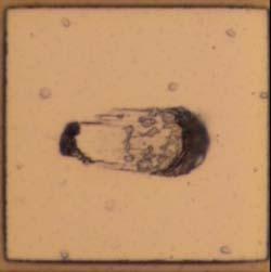


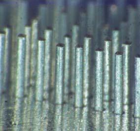
23 Probe Card Technologies Technology Cantilever Example Probe Mark Vertical Conventional VPC WSP Pogo Pin B. Mair and D. Copeland 23
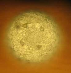
 High RF Example")

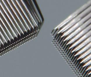
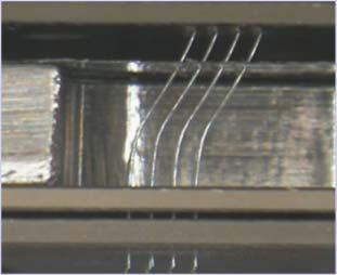
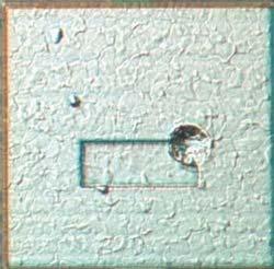
24 Recent Quals Ultra High Temp Cu Pillar Probing High Voltage (>1KV) High RF Example of Cu pillar structures. Example of Cu Pads probed with a WSP technology. B. Mair and D. Copeland 24
25 Probe Test Solution Specifications / Documentation B. Mair and D. Copeland 25
26 ` Probe Card Build Spec Released Probe Card Build Spec This document is to provide guidelines for probe card vendors on specifications to build probe cards Example Info from Spec: TI Mounting Standard table highlights different mounting hardware available for use with WCSP products Diagram shows that the build direction of the probes for cantilever cards must either be straight or all diagonal. No mixing of straight and diagonal builds. Cantilever Acceptance Guidelines recently added to place some general guidelines when cantilever versus vertical technology makes sense. B. Mair and D. Copeland 26
27 Design Review Process Flow Probe Cards Probe Card Design SUBMIT DRB Data Review Pass API Test Probe Card DRB Program Review Pass Production Release Fail Fail Resolve Issues Update Docs Benefits to Test Sites: The PBD provides TI Test Groups with the documentation needed to repair, maintain, and order new builds for production probe cards Onsite repair reduces tester downtime and offsite repair time Dual sourcing of New Orders and Rebuilds help control cycle time and cost. Benefits to TI: All probe card documentation resides in TI systems Accurate build data reduces build errors and avoids reverse engineering. Having the information needed to complete the order helps vendors control their cycle times. B. Mair and D. Copeland 27


28 Probe Card Build Data PBD Sources and Benefits The Probe Build Document (PBD) provides the details required to build TI s Probe Cards Today Probe Card build data is scattered across multiple documents until combined in the PBD. PBD Sources: Arc, ChipOpt, Cadence, M/B diagram; Vendor; etc Once Completed and released on EDGE, it is ready for review by a TI test site Test Site Design Review PBD Benefits: Design For Probe Support Multiple Suppliers Design data for new technology Repair/Maint support at test sites EDGE Release Complete PBD Finalized B. Mair and D. Copeland 28
29 What are the benefits of Design For Probe Process??? We are a support organization that has constant communication with the various pieces required for probe card solution. Probe Card Tech Tester Dev Prober Mech Interface Meet on a weekly basis with test floors to get feedback and discuss any issues that have surfaced as well as any new qualifications / optimizations that are taking place. We maintain many specifications that help to provide the outline for how probe card should be designed. ISMI External Benchmarks LBE Die /Test Req ds Wafer Probe Solution Adv Package Req ds WPL/PCB Test Flr Operations Infra-HW Interface with WPL and PC vendors so can help work through issues where cards not performing as should and make sure communicated back to vendors Utilizing the DFP team and its resources helps to provide the most optimal robust probe solutions for TI! 29 B. Mair and D. Copeland
30 Questions Brandon Mair Probe Test Solutions Engineer WW MAKE PTS Probe Test Solutions TEXAS INSTRUMENTS, INC Office: (214) Cell: (469) B. Mair and D. Copeland 30
31 Thanks! DFP Team Dawn Copeland Al Wegleitner Piper Oostdyk Dale Anderson Harry Singh Walt Edmonds TI BUs TI Test Floors The many probe card vendors we interface with! B. Mair and D. Copeland 31