Growth of monocrystalline In 2 O 3 nanowires by seed orientation dependent vapour-solid-solid mechanism
|
|
|
- Maude Freeman
- 5 years ago
- Views:
Transcription
1 Electronic Supplementary Material (ESI) for Journal of Materials Chemistry C. This journal is The Royal Society of Chemistry 2014 Electronic Supplementary Information (ESI) Growth of monocrystalline In 2 O 3 nanowires by seed orientation dependent vapour-solid-solid mechanism Sven Barth *, a, Michael S. Seifner a and Johannes Bernardi b Experimental procedure The alkoxide precursor, [In(O t Bu) 3 ] 2, was synthesized following a reported procedure. 1 The alkoxide was purified by sublimation at 90 C (10-3 mbar) and characterised by NMR. All experimental manipulations were performed in a modified Schlenk type vacuum assembly, taking stringent precautions against atmospheric moisture. Tert-butyl alcohol (Fluka), hexamethyldisilazane (ACROS) and solvents used for the synthesis were purified and dried by standard methods and stored over molecular sieves. Indium oxide nanowire synthesis was carried out in a horizontal CVD reactor in which a high frequency field was used to inductively heat the substrates (Au coated Si and Al 2 O 3 ) by placing them on a graphite susceptor ( o C). Substrates were coated with a 1 nm thick Au layer by sputtering. The thickness of Au films was precisely monitored using a quartz microbalance. [In(O t Bu) 3 ] 2 was introduced in the reactor through a glass flange by applying dynamic vacuum (10-3 mbar) and heating the precursor reservoir to the desired temperature (75-80 o C). The solid precursor was always used in powder form without bigger crystallites to ensure similar vapour pressure. For the growth of nanowires 30 mg [In(O t Bu) 3 ] 2 was used and the growth duration was 120 min. Slow evaporation is crucial to obtain nanowire growth in the investigated low temperature range. A similar arrangement for the use of molecular species to grow thin films on inductively heated large substrates was described in a previous paper. 2 The morphology of 1D nanostructures was analysed using a FEI Inspect F50 scanning electron microscope (SEM). The nanowires were deposited on lacey carbon and carbon film copper grids for TEM characterisation (Alfa Aesar) using mechanical force. In this study, a FEI TECNAI F20 operated at 200 kv and equipped with high angle annular dark field (HAADF) STEM and EDX detector was used. The images were recorded and treated using Digital Micrograph software.
![Weight [%] 110 100 90 80 70 60 50 40 30 20 10 0 100 200 300 400 Temperature [ C] S1: The thermogravimetric analysis of the [In(O t Bu) 3 ] 2 shows the single-step decomposition of the precursor at](/docs-images/89/100208113/images/2-0.jpg "190-210 C. The resulting mass is very close to the theoretical value 38 % for a conversion to pure In 2 O 3.")
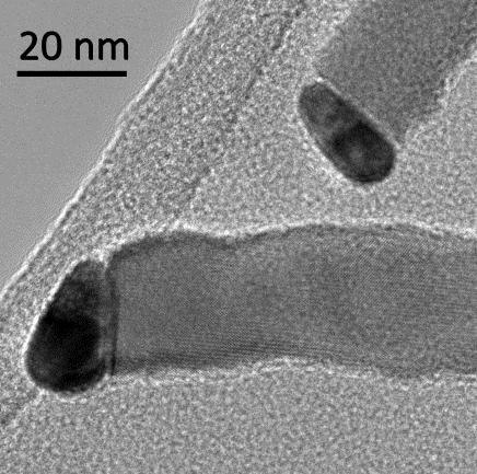
2 Weight [%] Temperature [ C] S1: The thermogravimetric analysis of the [In(O t Bu) 3 ] 2 shows the single-step decomposition of the precursor at C. The resulting mass is very close to the theoretical value 38 % for a conversion to pure In 2 O 3. The initial mass loss is due to the partial hydrolysis of the alkoxide by the nitrogen gas used. S2: TEM image of an indium oxide nanowire grown at 500 C with secondary film formation towards the nanowire base (1 µm from the growth seed) leading to tapering of the nanowires.

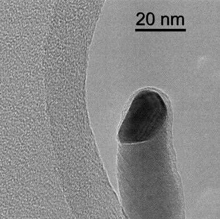
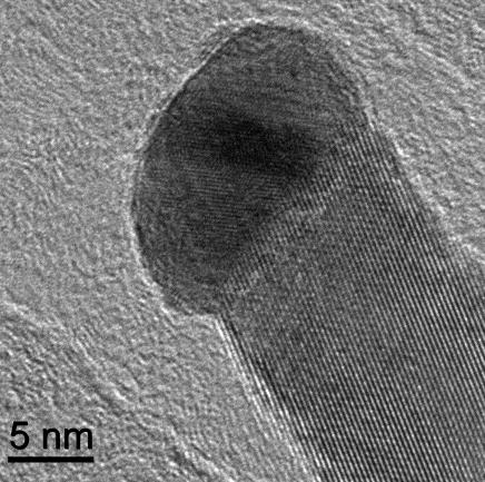
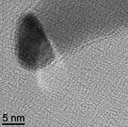
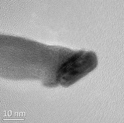
3 S3: The TEM images show the different non-hemispherical shapes of the growth seeds leading to the conclusion that the particles are solid during the In 2 O 3 nanowire growth.
.")


4 a) b) c) S4: The EDX spectrum of the nanowire tip in (a) reveals the non-alloyed Au growth seed, which is illustrated in (b). The red frame highlighted with the arrow shows the location of the probed sample. The HAADF image in (c) is clearly showing the small diameter of the nanowires obtained and also the gold growth seeds terminating the wires tips are clearly visible by the Z-contrast.
 In 2")
 (0 44) Au")

5 a) 45 Au (200) nm Au (100) In 2 O 3 (400) In 2 O 3 (2 22) (0 44) Au (200) In 2 O 3 (440) [011] In 2 O 3 zone axis b) 56
 S5: The HRTEM images show more examples of the orientation dependent lattice matching of the Au growth seeds and the indium oxide nanowire.")
 Au (100) in an angle of 45 to a smooth interface 0.574 nm effective spacing five Au (100) to four In 2 O 3 (110) with 0.716 nm 0.")
6 c) nm Au (111) Au (200) (222) In 2 O nm In 2 O 3 (222) S5: The HRTEM images show more examples of the orientation dependent lattice matching of the Au growth seeds and the indium oxide nanowire. According to the widening of the lattice fringes at the interface due to the tilting and with the assumption of a smooth interface between both materials, the following mismatches can be calculated: a) Au (100) in an angle of 45 to a smooth interface nm effective spacing five Au (100) to four In 2 O 3 (110) with nm 0.2 % lattice mismatch b) Au (100) in an angle of 56 to a smooth interface nm effective spacing nine Au (111) to ten In 2 O 3 (400) with nm 0.5 % lattice mismatch c) Au (100) in an angle of 40 to a smooth interface nm effective spacing five Au (111) to four In 2 O 3 (222) with nm (inclined by 60 ; original spacing nm) 0.9 % lattice mismatch


7 a) b) c) d) Figure S6: Heat treated single crystal surfaces and resulting nanostructure nucleation on (a-b) (0001) c-plane sapphire and (c-d) (1120) a-plane sapphire. The gold thickness was 0.2 nm and the heat treatment was at 750 C for 15 min. References: 1. S. Suh and D. M. Hoffman, Journal of the American Chemical Society, 2000, 122, S. Mathur, S. Barth and H. Shen, Chem. Vapor Depos., 2005, 11,