Amorphous silicon thin film solar cells
|
|
|
- Marsha Heath
- 5 years ago
- Views:
Transcription
1 Amorphous silicon thin film solar cells c-si a-si large concentration of intrinsic defects N T >10 16 cm -3 ( dangling bonds D +, D -, D o ) doping more difficult, e.g. if we increase a number of free electrons by adding P the concentration of D - defects increases also passivation of defects by hydrogen a-si:h - decreases N T to ~10 15 cm -3 doping and creation of pn junction becomes possible! 1
2 Absorption in a-si direct bandgap 1.7 ev, E g >E g (c-si) no well-defined E(k) dependence no conservation of momentum k absorption coefficient ~ times higher thin film solar cell cell (~5 µm) possible λ(µm) 2

3 Gap states in a-si D - D + very high density of defect levels in the gap doping not effective passivation of defects by hydrogen doping possible in Si:H! 3
4 Steabler-Wronski effect device degradation: efficiency loss due to photo-generation of defects power Best modules: η=10.5 % (stabilized) Problem: more degradation when more Si-H 2 bonds present 4

5 Deposition process rf PECVD deposition system large area deposition (more than 1 m2) low deposition temperature (100 C < Ts < 400 C) use of any cheap and arbitrarily shaped substrates effective p- and n-type doping and alloying deposition of composition-graded layers deposition of multi-layer structures by control of gas mixtures in a continuous process easy patterning and integration technology low cost good mass-producibility 5
6 a-si cell parameters short diffusion length ~100 nm and decreases more with doping minority carrier lifetime 10 ns solution: p-i-n cell extended electric field region Jsc Voc Fill factor Efficiency [ma/cm2 [V] [%] UNSW mono c-si PERL structure USSC a-si:h p-i-n structure 6


7 a-si cell basic design p-i-n cell p i n band diagram Thin doped regions reduced degradation TCO - transparent conducting oxide (ZnO, SnO 2 ) 7
 laser scribing sputtering SiH4, glow discharge process metalization, laser scribing, polymer coating")
8 a-si solar cell Fabrication steps: TCO (spray deposition) laser scribing p-asi (10 nm) i-a-si (500 nm) n-asi (10 nm) laser scribing sputtering SiH4, glow discharge process metalization, laser scribing, polymer coating 8
9 HIT solar cells (Heterojunction with intrinsic thin layer) Sanyo good surface passivation low temperature processing (<200 C) η= 25,6% modules up to 19% 9


10 Multijunction devices double junction better stability 10
11 Thin film heterojunction solar cells window(e g1) absorber (E g2 ) polycrystalline materials good absorption properties 2-5 µm absorbers p-n heterojunctions low costs, low energy- and material -consuming technologies 100 x less material than for c-si 11
12 Heterojunction photovoltaic structure advantages: maximum generation in the electric field region of absorber: no problem with front surface recombination disadvantages: interface recombination, band edge discontunuities at interface CdTe, Cu(In,Ga)Se 2 absorber E g2 CdS, Zn(O,S), In 2 S 3...,.. okno window 3... absorber: bandgap close to 1.5 ev p-type doping ~10 16 cm -3 high absorption coeffient p 2 µm E g1 n window: large bandgap (transparent) good conduction band alignement with absorber n-type doping cm -3 12
13 Heterojunction advantages of window-absorber concept pn junction heterojunction E E Max. generation density of e-h pairs at the front surface surface recombination losses necessity of surface passivation Generation at maximum outside of the juntion field Max. generation density in the absorber far from the front surface in the region of maximum electric field 13
14 Current transport in the heterojunction o recombination in the bulk of absorber o recombination via interface states o tunnelling to interface states Conduction band alignement cliff spike bad: loss in the barrier height increased interface recombination bad: barrier for photoelectrons 14
15 Material requirements absorber direct bandgap E g 1.4 ev p-type electrical conductivity high diffusion barrier long diffusion length window high energy gap high conductivity good ohmic electrical contacts similar lattice constants good band alignement stable junction availability and low cost of materials and technology low toxity of materials There is not so many materials meeting these requirements! Highest efficiencies achieved with CIGS and CdTe-based solar cells 15
16 Semiconducting chalcopyrites from CIGS family direct bandgap, very high absorption coefficient CuInSe 2 E g = 1.04 ev CuGaSe 2 E g = 1.68 ev CuInS 2 E g = 1.55 ev Solid solutions Cu(In,Ga)Se 2 i CuIn(Se,S) 2 Highest efficiency (record 22.3%) achieved with CuIn 1-x Ga x Se 2 x = E g = 1,12-1,20 ev 16
17 CuGa x In 1-x Se 2 solid solutions as absorbers Lower efficiency for Ga/(In+Ga)>0.3 Bad conduction band alignement? 17
 n-cds (50 nm) p-cuin 1-x Ga x Se 2 (2 µm) Mo ncds buffer good alignement of conduction bands lattice constant matches that")
18 Baseline CIGS device window buffer n + - ZnO:Al (0.3 µm) i - ZnO (0.1 µm) n-cds (50 nm) p-cuin 1-x Ga x Se 2 (2 µm) Mo ncds buffer good alignement of conduction bands lattice constant matches that of CIGS electrochemical treatment of the absorber surface 18

19 CIGS cell band diagram 3.4 ev absorber buffor okno 19
20 ZnO - sputtering CdS - CBD (chemical bath deposition) Cu(In,Ga)Se 2 - co-evaporation - selenization of metal layers in Se lub H 2 Se vapour - bilayer, 3 stage process, Mo - RF sputtering soda-lime glass 20
21 Preparation of CIGS absorber layer 21
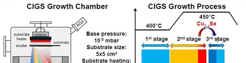
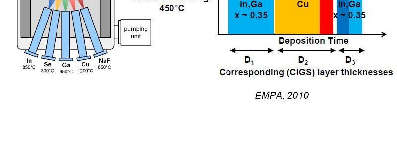
22 Absorber preparation- 3 stage process 22

23 Grain boundaries in CIGS c GB Si i GaAs GB v c Grain boundaries in CuInSe 2 GB v h + in CIGS neutral grain boundaries, lower E v? policrystalline material makes better cells than single crystal segregation of impurities at GB? 23
24 Native defects and doping Specific problems p-doping by Cu vacancies: Cu-poor composition Cu/(In+Ga)<1 large concentration of native defects: Se vacancies, In Cu antisites, etc large deviation from stechiometry (Cu/(In+Ga) down to 0.8) tolerated! metastable changes of photovotaic parameters light soaking improves the efficiency! Influence of sodium diffusing from soda-lime glass Na increases net doping and improves morhology of the layer: grain boundaries passivated? compensating donors passivated? growth improved by better incorporation of Se (Na 2 Se topotaxy)? NaF source of sodium when deposition on sodium-free substrate Cd-free buffers: worse performance (???) Zn(Mg)O by ALD, Zn(O,S) by CBD and In x S y by PVD almost as good as CdS 24
25 Metastabilities of junction parameters morning sickness current [ma] K -30 0,2 0,4 0,6 0,8 voltage [V] I-V after a long time in darkness - I-V after white light soaking: V oc and FF improves! Recent theoretical and experimental findings: specific properties of V Se and In Cu- related defects 25
")

26 Flexible substrates 20.4% on polyimide foil (2013) EMPA (Switzerland) NaF precursor provides neccesary sodium 26
 post-deposition treatment very thin CdS steep Ga gradient")
27 New record CIGS cell 22.6% ZSW Germany new alkali (Na,K) post-deposition treatment very thin CdS steep Ga gradient towards back electrode Modules with K-treatment 17.5% (Solibro, Sweden) 27


28 Stability irradiation by proton flux s exceptionally good if protected against humidity radiation hardeness more than 1 order of magnitude better than crystalline absorbers good for space application! 28
29 Kesterites new photovoltaic materials remedy for shortage of indium, earth-abundant matrials CuIn InSe 2 Eg=1.5 ev Cu 2 ZnSn(S,Se) S,Se) 4 η=12.6% (IBM ( 2014) (from hydrazine solution) Problems: many secondary phases very defected material 29
 superstrate configuration absorber: CdTe 3-5 µm intrinsic p-type doping ~10 15 cm -3 direct")
30 CdS/CdTe heterojunction solar cell efficiency 22.6 (First Solar 2016) (modules up to 18.6%) superstrate configuration absorber: CdTe 3-5 µm intrinsic p-type doping ~10 15 cm -3 direct bandgap Eg =1.5 ev 30
 CSS Solar Cell Inc. (USA) 15.8 / 1.05 cm 2 8.4 / 7200 cm 2 electrodeposition BP Solar 14.2 / 0.")
31 Absorber preparation: CdTe: PVD, CSS, electrodeposition, spray pyrolysis CdCl 2 treatment at T>400 C: recrystallisation of CdTe grains passivation interface improvement Close space sublimation process ohmic back contact: difficult Cu-Au alloy or ZnTe:Cu, Sb 2 Te 3, s process company efficiency(%) CSS Solar Cell Inc. (USA) 15.8 / 1.05 cm / 7200 cm 2 electrodeposition BP Solar 14.2 / 0.02 cm / 706 cm 2 Screen printing Matsushita 12.8 / 0.78 cm / 1200 cm 2 Spray pyrolysis Golden Photon 12.7 / 0.3 cm / 832 cm 2 VTD First Solar 18,6 / 1200 cm 2 sputtering 10.4 / 0.1 cm 2 31
32 Life cycle assesment of Cd Cd is a by product of production of metals from zink ores (~80%) and lead ores (~20%) (from wastes) V.M. Fthenakis g of Cd per GWh during life time of CdTe module power plants based on coal emit minimum of 2 g of Cd/GWh! 32