Low Temperature Atomic Layer Deposition of Tin Dioxide, SnO\(_2\)
|
|
|
- Myrtle Arnold
- 5 years ago
- Views:
Transcription
1 Low Temperature Atomic Layer Deposition of Tin Dioxide, \(_2\) The arvard community has made this article openly available. Please share how this access benefits you. Your story matters Citation eo, Jaeyeong, Adam S. ock, and Roy G. Gordon Low temperature atomic layer deposition of tin dioxide, \(_2\). Presentation slides. 10th International Conference on Atomic Layer Deposition. Seoul, South Korea. Citable link Terms of Use This article was downloaded from arvard University s DAS repository, and is made available under the terms and conditions applicable to ther Posted Material, as set forth at nrs.harvard.edu/urn-3:ul.instrepos:dash.current.terms-ofuse#laa
2 Low Temperature Atomic Layer Deposition of Tin Dioxide, 2 Jaeyeong eo, Adam S. ock and Roy G. Gordon arvard University Cambridge, MA USA arvard University
3 utline Earth-abundant, non-toxic transparent conductor: 2 ALD process for 2 new tin precursor growth per cycle 2 film properties composition structure optical properties p electrical properties applications arvard University 2
4 2 : Transparent Conductor and eat Mirror igh visible ibl transmission i (high h bandgap (E g ~ 4.1 ev) igh electrical conductivity (high electron concentration and mobility) igh environmental stability Constituent elements are non-toxic and abundant Known ALD processes require high temperatures, > 200 o C or produce impure films (C, N), amorphous, low conductivity arvard University 3
5 Tin(II) Cyclic Stannylene as ALD Precursor t-bu N N t-bu N 2,N 3 -di-tert-butyl-butane-2,3-diamido-tin(ii) ydrocarbon ligand => high volatility (30 Torr at 60 o C) Chelate structure => thermal stability -N bonds => reactive to hydrogen peroxide, 2 2 Synthesis and properties described by Adam ock, Wednesday 14:15 arvard University 4
6 ALD Process for 2 Source temperature: 40 o C Growth per cycle: 0.18 nm Substrate temperature: 120 o C Induction period: only a few cycles 80 Thickne ess (nm) Cycles arvard University 5
7 ALD Saturation Curves Increasing doses of cyclic stannylene precursor for tin Increasing doses of oxygen precursor, hydrogen peroxide Refractive index ~ 1.94 for saturated growth (3 doses) arvard University 6
8 Temperature Dependence of Growth 0.20 Dep osition Rat te (nm/cyc le) Temperature ( o C) ALD window from 50 to 150 o C arvard University 7
9 x Composition Rutherford Backscattering Spectroscopy (RBS) ield Normalized Yi Carbon Substrate Energy (MeV) C in film N Channel No C or N in film o / Rati As-depo o C anneal Number of 2 2 doses 2 for 2-3 doses arvard University 8
10 X-Ray Photo-Electron Spectroscopy (XPS) No impurities detected (C, N) inside film arvard University 9


11 Smooth Morphology of 2 Films x 2 Si 2 µm nm Si nm 200nm µm AFM 400 cycles => 71 nm RMS roughness = 2 nm < 3 % of thickness arvard University 10


12 Step Coverage Uniform thickness in holes with aspect ratio 50:1, grown at 50 o C arvard University 11
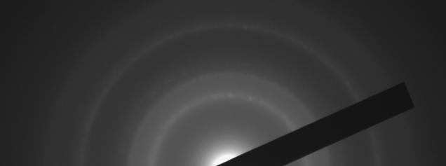


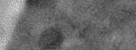


13 Polycrystalline Rutile Structure of 2 Films TEM Si (110) (211) (101) (301) (200) electron diffraction 5 nm 2 X-Ray Diffraction (XRD) arvard University 12
14 2 has Very Little Visible Absorption Transmission n & Reflection T R Wavelength (nm) absorption = 1-T-R Wavelength (nm) film 100 nm thick Band gap 4.13 ev nt 2 (cm -2 ) absorptio on coefficie 5x x x x x E (ev) arvard University 13
15 Electrical Properties >10 5 Resistivity minimum for stoichiometric 2 (2 to 4 doses) Resistivity ( cm) Number of 2 2 doses N-type semiconductor by all measurements electron concentration ~ cm -3 electron mobility ~ 6 cm 2 V -1 s -1 arvard University 14
16 Resistivity vs. Deposition Temperature m) Resisti ivity ( -cm 6x10⁻² 5x10⁻² 4x10⁻² 3x10⁻² 2x10⁻² (b) Temperature ( o C) minimum i resistivity it cm when deposited d at 120 o C arvard University 15
17 Proposed Mechanism Ligand exchange of precursor with hydroxylated surface t-bu N N t-bu t-bu N N t-bu t-bu N N t-bu xidative addition of hydrogen peroxide arvard University 16
18 Summary 2 is transparent semiconductor made of earth-abundant, abundant, inexpensive, non-toxic elements ALD from a cyclic tin(ii) amide and 2 2 => 2 Smooth films of pure, stoichiometric, polycrystalline 2 igh optical transparency and electrical conductivity Successfully used in several applications: organic solar cells (with Alan eeger, UCSB) conducting and protective coatings for plastics (with Michelle Schulberg, Physical Sciences Inc.) electron multipliers (Philippe derouffignac, Arradiance, to be presented on Wednesday at 13:30) another possible application: thin-film transistors on plastic arvard University 17
19 Acknowledgements all measurements done with Mark Winkler and Eric Mazur Support was provided by the following: Camille and enry Dreyfus Postdoctoral Program in Environmental Chemistry Air Force ffice of Scientific Research-STTR under contract FA C-0075 Center for Nanoscale Systems (CNS), a member of the National Nanotechnology Infrastructure Network (NNIN), which is supported by the National Science Foundation under NSF award no. ECS CNS is a part of the Faculty of Arts and Sciences and the School of Engineering and Applied Sciences at arvard University. arvard University 18