To explore the ability of the DVD technology to create dense, pinhole-free metal oxide
|
|
|
- Alexander Byrd
- 5 years ago
- Views:
Transcription
1 Chapter 4 Results 4.1 Strategy To explore the ability of the DVD technology to create dense, pinhole-free metal oxide layers and to develop an initial understanding of the relationship between various DVD processing conditions and deposited film properties, especially film density, the experiments outlined in Table 3.2 have been conducted. For the numerous results presented in this chapter, the figure captions will refer to the experiment numbers listed in Table 3.2. During each experiment, the process chamber pressure and the pressure in the carrier gas mixing chamber prior to the nozzle (See Fig. 1.4.) were recorded. For all experiments, these pressures were 8.0 Pa / 60 mtorr in the process chamber and 56 Pa / 420 mtorr in the carrier gas mixing chamber. The introduction of a small amount of argon through the plasma hollow cathode during select experiments generated only a nominal rise in these readings. 48
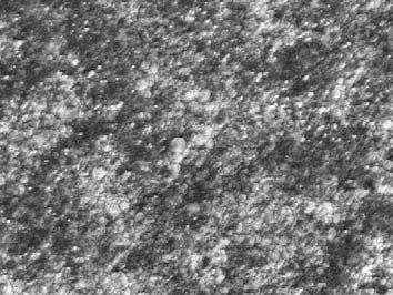
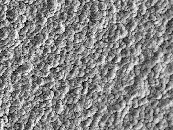
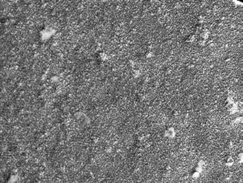
2 Deionized water test pictures After each DVD film was deposited, the sample was removed from the sample holder in the deposition chamber, and a deionized water test was immediately performed. The results of these water tests could be grouped into three categories. For samples 1, 2 and 3, the deionized water droplet soaked into the deposited film as soon as it was placed on the surface, suggesting a porous deposit (Fig 4.1). For samples 4 and 5, the deionized water droplet did not soak into the deposited film immediately. Rather the droplet spread out broadly across the film surface and absorbed into the film over a span of several minutes (Fig 4.2). This suggested that the DVD process conditions of these experiments had created a slightly denser film. For samples 6, 7 and 8, the deionized water droplet remained on the film surface for at least ten minutes, suggesting that these DVD deposits were the densest of all (Fig 4.3).


3 50 Figure 4.1 Deionized water test of sample 3. film quickly. Porous film, water penetrates through Figure 4.2 Deionized water test of sample 4. the film after several minutes. Denser film, water penetrates through

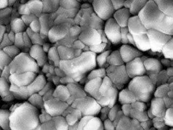
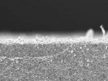
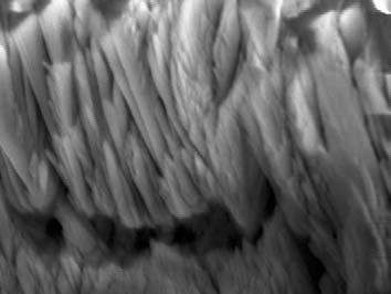
4 51 Figure 4.3 Deionized water test of sample 6. deposited film for 10 minutes. Dense film, water stays on top of the 4.3 SEM and XRD analysis of deposited films SEM and XRD analysis was designed to provide additional insight into the atomic structure of deposited films Analysis of Sample 1 Creation of this sample employed the experimental constants listed in Table 3.1 to deposit material onto an as-received anode substrate. No plasma activation or substrate biasing was employed. The SEM images and XRD results from this sample are shown in Figs
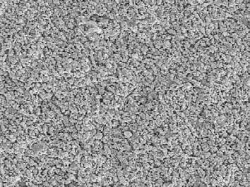
5 52 Figure 4.4 Top (deposition) surface of sample 1, 400x. 100 µm 10 µm Figure 4.5 Top (deposition) surface of sample 1, 3000x. This image reveals a highly faceted deposition surface.

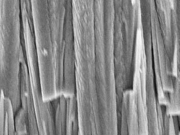
6 53 2 µm Figure 4.6 Top (deposition) surface of sample 1, 8000x. Large gaps (pores) are clearly visible between the faceted YSZ deposits. 100 µm Figure 4.7 Cross-section of sample 1, 400x. The deposited coating is approximately 120 µm thick, with clearly defined growth columns.
7 54 Figure 4.8 Cross-section of sample 1, 4000x. 5 µm Figure 4.9 XRD scan of sample 1. The x-ray diffraction scan reveals peaks for yttria-stabilized zirconia. The peak locations are consistent with cubic YSZ.
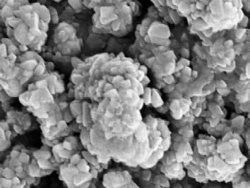
8 Analysis of Sample 2 Creation of this sample employed the experimental constants listed in Table 3.1 to deposit material onto an as-received anode substrate while also running the DVD plasma unit with a 60 A current. No substrate bias was applied to the sample during deposition. The SEM images and XRD results for this sample are shown in Figs Figure 4.10 Top (deposition) surface of sample 2, 400x. 100 µm
 betweeen YSZ")
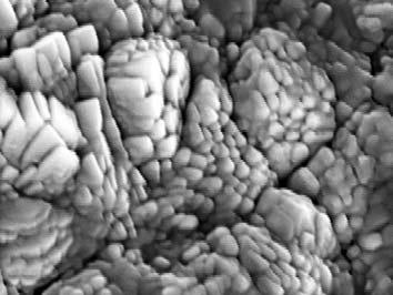
9 56 10 µm Figure 4.11 Top (deposition) surface of sample 2, 3000x. The faceted columns of sample 1 have been replaced by a cauliflower-like rough surface with apparent gaps (pores) betweeen YSZ deposits. Figure 4.12 Top (deposition) surface of sample 2, 8000x. 2 µm
10 µm Figure 4.13 Cross-section of sample 2, 400x. The deposited coating is approximately 84 µm thick. 5 µm Figure 4.14 Cross-section of sample 2, 4000x.
11 58 Figure 4.15 XRD scan of sample 2. This scan reveals the peaks for yttria-stabilized zirconia and nickel oxide (presumably from the anode substrate). The peaks for the nickel oxide are labeled s for substrate Analysis of Sample 3 Creation of this sample employed the experimental constants listed in Table 3.1 to deposit material onto an as-received anode substrate while also running the DVD plasma unit with a 60 A current and 50 V DC - substrate bias. The SEM images and XRD results from this sample are shown in Figs
 surface of sample 3, 400x.")
 surface of sample 3, 3000x.")
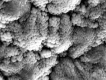
12 59 Figure 4.16 Top (deposition) surface of sample 3, 400x. 100 µm 10 µm Figure 4.17 Top (deposition) surface of sample 3, 3000x. visible between finely textured YSZ deposits. Gaps (pores) are clearly
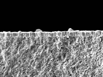
13 60 2 µm Figure 4.18 Top (deposition) surface of sample 3, 8000x. 100 µm Figure 4.19 Cross-section of sample 3, 400x. The deposited coating is approximately 30 µm thick.
14 61 Figure 4.20 Cross-section of sample 3, 4000x. 5 µm Figure 4.21 XRD scan of sample 3. This scan reveals peaks for yttria-stabilized zirconia, nickel oxide, and zirconia. The peaks for the nickel oxide are labeled s while the zirconia peaks are labeled z.

15 Analysis of Sample 4 Creation of this sample employed the experimental constants listed in Table 3.1 to deposit material onto an as-received anode substrate while also running the DVD plasma unit with a 120 A current and 50 V DC - substrate bias. The SEM images and XRD results from this sample are shown in Figs Figure 4.22 Top (deposition) surface of sample 4, 400x. 100 µm

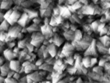
16 63 Figure 4.23 Top (deposition) surface of sample 4, 3000x. open porosity is again visible. 10 µm YSZ deposits between 2 µm Figure 4.24 Top (deposition) surface of sample 4, 8000x.
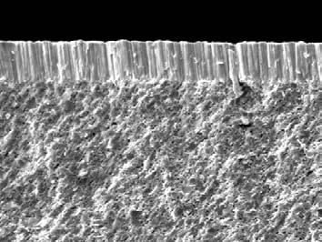
17 µm Figure 4.25 Cross-section 400x - sample 4. The deposited coating is approximately 20 µm thick. Introduction of plasma activation and substrate biasing is leading to reduced coating thicknesses. Figure 4.26 Cross-section of sample 4, 4000x. 5 µm
18 65 Figure 4.27 XRD scan of sample 4. Peaks are visible for YSZ and nickel oxide ( s ) Analysis of Sample 5 Creation of this sample employed the experimental constants listed in Table 3.1 to deposit material onto an as-received anode substrate while also running the DVD plasma unit with a 120 A current and 200 V DC - substrate bias. The SEM images and XRD analyses of this sample are shown in Figs
 surface of sample 5, 3000X.")
19 66 Figure 4.28 Top (deposition) surface of sample 5, 400x. 100 µm 10 µm Figure 4.29 Top (deposition) surface of sample 5, 3000X. Porosity is visible between deposits of YSZ but not as distinctly as in Fig

20 67 Figure 4.30 Top (deposition) surface of sample 5, 8000x. 2 µm 100 µm Figure 4.31 Cross-section of sample 5, 400x. The deposited coating is just 15 µm thick.
21 68 Figure 4.32 Cross-section of sample 5, 4000x. 5 µm Figure 4.33 XRD scan of sample 5. zirconia ( z ). Peaks are visible for YSZ, nickel oxide ( s ), and
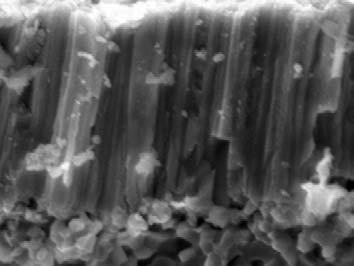
22 Analysis of Sample 6 Creation of this sample employed the experimental constants listed in Table 3.1 to deposit material onto an as-received anode substrate while also running the DVD plasma unit with a 120 A current and 200 V AC substrate bias. The SEM images and XRD results for this sample are shown in Figs Figure 4.34 Top (deposition) surface of sample 6, 400x. 100 µm
 surface of sample 6, 3000x.")

23 70 10 µm Figure 4.35 Top (deposition) surface of sample 6, 3000x. The appearance of this deposition is similar to that of sample 3, but at a different length scale. (See Fig ) Figure 4.36 Top (deposition) surface of sample 6, 8000X. 2 µm
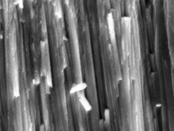
24 µm Figure 4.37 Cross-section 400x - sample 6. The deposited coating is just 13 µm thick. 5 µm Figure 4.38 Cross-section of sample 6, 4000x. The deionized water test suggests that this columnar film is dense enough to resist water penetration.
25 72 Figure 4.39 XRD scan of sample 6. zirconia ( z ). Peaks are visible for YSZ, nickel oxide ( s ), and Analysis of Sample 7 Creation of this sample employed the experimental constants listed in Table 3.1 to deposit material onto a polished anode substrate while also running the DVD plasma unit with a 120 A current and 200 V AC substrate bias. The SEM images and XRD analyses of this sample are shown in Figs
26 µm Figure 4.40 Top (deposition) surface of sample 7, 400x. 10 µm Figure 4.41 Top (deposition) surface of sample 7, 3000x. Porosity appears evident between growth columns.

27 74 Figure 4.42 Top (deposition) surface of sample 7, 8000x. 2 µm 100 µm Figure 4.43 Cross-section of sample 7, 400x. The deposited coating is just µm thick.
28 75 5 µm Figure 4.44 Cross-section of sample 7, 4000x. Figure 4.45 XRD scan of sample 7. zirconia ( z ). Peaks are visible for YSZ, nickel oxide ( s ), and

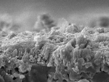
29 Analysis of Sample 8 Creation of this sample employed the experimental constants listed in Table 3.1 to deposit material onto a polished anode substrate while also running the DVD plasma unit with a 180 A current and 200 V AC substrate bias. The SEM images and XRD analyses of this sample are shown in Figs Figure 4.46 Top (deposition) surface of sample 8, 400x. 100 µm
30 77 Figure 4.47 Top (deposition) surface of sample 8, 3000x. 10 µm 2 µm Figure 4.48 Top (deposition) surface of sample 8, 8000x. in this thin YSZ deposit. Porosity is clearly evident
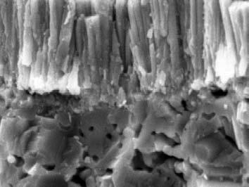
31 78 film substrate 100 µm Figure 4.49 Cross-section of sample 8, 400x. The deposited coating is just 5 µm thick. film substrate 5 µm Figure 4.50 Cross-section of sample 8, 4000x.
32 79 Figure 4.51 XRD scan of sample 8. zirconia ( z ). Peaks are visible for YSZ, nickel oxide ( s ), and SEM image comparison To faciliate comparison of atomic structures between samples, the SEM images presented on the previous pages are reproduced in the following Figures 4.52 through 4.56.


33 Figure 4.52 Top (deposition) surface of all samples, 400x.

")

34 Figure 4.53 Top (deposition) surface of all samples, 3000x.


35 Figure 4.54 Top (deposition) surface of all samples, 8000x.


36 Figure 4.55 Cross-section of all samples, 400x.


37 Figure 4.56 Cross-section of all samples, 4000x.
38 XRD results summary For the yttria-stabilized zirconia detected in each sample, Table 4.1 records the peak positions for the cubic YSZ observed in each of the eight samples. The table also shows the comparable reference data from the literature for Y 0.15 Zr 0.85 O 1.93 [69]. Table 4.2 records the normalized XRD peak intensities (I) with respect to the height of the {111} peak in each sample. Peak heights for a randomly oriented YSZ sample are also presented for comparison. While no discernible texture preference is evident, the deposited samples also have not grown in a purely random manner. It is interesting to note the change in preferred growth between samples 6 and 7 in which the only difference between experiments was the condition of the substrate, as-received versus polished. Table 4.1: Peak positions (d spacings) from XRD patterns of the YSZ films deposited with different process conditions (in Angstroms) Sample {111} {200} {220} {311} {400} Reference
39 86 Table 4.2: Relative peak intensities from XRD patterns of the yttria-stabilized zirconia films deposited with different process conditions Sample I {111} I {200} I {220} I {311} I {400} Random Summary The results of this chapter suggest that DVD plasma activation and substrate biasing can increase film density. The XRD results show that the deposited film has the same crystal structure as the vapor source. A more detailed examination of the results of this study will be presented in Chapter 5 Discussion.