Laser processing of TiO 2 films on ITO-glass for
|
|
|
- Clemence Pope
- 5 years ago
- Views:
Transcription
1 Laser processing of TiO 2 films on ITO-glass for Dye-sensitized solar cells A thesis submitted to the University of Manchester for the degree of Doctor of Philosophy in the Faculty of Science and Engineering 2017 Aseel Abdulkreem Hadi School of Materials 1
2 Table of Contents List of Tables... 7 List of Figures... 8 List of Abbreviations and Symbols Abstract Declaration Copyright statement Acknowledgements Chapter 1. General Introduction Background and Rationales Aims and Objectives of the Research Thesis outlines Chapter 2. Literature Review Introduction Solar cells and Photovoltaic Effect Dye sensitised solar cells Components of DSSCs Working Principle of DSSCs Mesoporous semiconductor thin films Mesopourous TiO Mesoporous TiO 2 thin films in DSSCs Blocking layers Synthesis methods for mesoporous TiO 2 thin films Screen printing or Doctor Blade Other methods Sintering process for mesoporous TiO 2 thin film formation Standard conventional thermal method Alternative methods Opportunities of using lasers for sintering Basic construction and principle operation of laser Laser beam Characteristics Industrial lasers Laser beam interaction with materials
3 Photo-thermal Processing (Lattice Heating) Photochemical Processing Spatial distribution of laser deposited energy Heat transfer mechanism by Laser Irradiation Influencing Factors in Laser processing Previous work on laser applications for DSSCs Sintering of the TiO 2 film Surface modification of furnace-sintered TiO 2 thin films Other laser processing for DSSCs Identified knowledge gaps...85 Chapter 3. Experimental Procedures and Characterization Techniques Introduction Chemicals and materials Preparation of TiO 2 paste Preparation of TiO 2 precursor Deposition of TiO 2 layers on ITO-glass Deposition of TiO 2 paste on ITO-glass Deposition of TiO 2 precursor on ITO-glass Deposition of TiO 2 paste on TiO 2 precursor deposited on ITO-glass Furnace sintering Furnace-sintering for formation of mesoporous TiO 2 films on ITO-glass Furnace-sintering for mesoporous TiO 2 and compact TiO 2 block layers on ITO-glass Excimer laser processing KrF Excimer laser Excimer laser processing Fibre laser processing Fibre laser Fibre laser sintering Temperature profile measurement Property measurement of TiO 2 paste TGA/DTGA measurement Optical property measurement Microstructural Characterization Evaluation of organic binder removal
4 Surface and cross sectional morphological observation Surface topographic measurement Cross sectional observation in depth Phase measurement X-Ray Diffraction XRD Raman Spectroscopy Surface chemistry analysis by X-ray photoelectron spectroscopy DSSC construction DSSC assembling Dye adsorption measurement Photovoltaic performance of DSSCs J-V characterisation Electrochemical impedance spectroscopy EIS characterisation Chapter 4. Surface Modification of as-sintered TiO 2 Thin Films by Excimer Laser Introduction Microstructural characterization of as-sintered TiO 2 thin films with and without Excimer laser treatment Surface morphology Surface Roughness Cross-sectional morphology Phase analysis Optical Characteristics Photovoltaic performance J-V Characteristics Electrochemical impedance spectroscopy Summary Chapter 5. Fibre Laser Fabrication of Mesoporous TiO 2 Thin Films on ITO Glass Introduction Thermal analysis of the TiO 2 paste Optical property measurement of the TiO 2 paste deposited on ITO-glass Initial observation of sintered TiO 2 films on ITO-glass by furnace and laser Temperature profiles of TiO 2 surface during laser sintering
5 5.5.1 Measurements of temperature profiles Analysis of organic binders within laser-sintered TiO 2 films on ITO-glass Laser sintering mechanism Microstructural characterisation of sintered TiO 2 films Surface morphology Surface Roughness Cross-sectional morphology Nano-structural Imaging by TEM Crystal structure and defects of TiO 2 films X-ray Diffraction (XRD) X-ray photoelectron spectroscopy (XPS) Photovoltaic performance J-V Characteristics Electrochemical impedance spectroscopy (EIS) Fibre laser sintering of thicker TiO 2 layers Summary Chapter 6. One-step laser sintering for Formation of TiO 2 Block Layer and Mesoporous TiO 2 Thin Films on ITO glass Introduction Temperatures profile of TiO 2 surface during laser sintering Crystal phase and defects analysis on the TiO 2 films Phase analysis Crystal defect analysis Microstructural characterization of compact TiO 2 and mp-tio 2 thin films Surface morphology of compact TiO 2 layers Surface morphology of mesoporous TiO 2 films Cross sectional view of TiO 2 -BLs and mesoporous thin films Photovoltaic performance of DSSCs J-V Characteristics EIS Characterization Summary Chapter 7. Conclusions and Future Work Conclusions Fibre laser sintering process
6 7.1.2 Excimer laser surface modification Future work References Publications Final Word Count: 62,589 6
7 List of Tables Table 2.1. Advantages of DSSCs in comparison with other semiconductor based solar cells, adopted from [27] Table 2.2. Photovoltaic parameters of the dye solar devices based TiO 2 photoanodes fabricated from various pastes, adopted from [104]...52 Table 2.3. Electron transport parameters, obtained from EIS results of DSSCs based on mp- TiO 2 sintered at different temperatures, adapted from [116] Table 2.4. Classification of industrial lasers, adapted from [139]...68 Table 3.1. The excimer laser parameters used for processing as-sintered TiO 2 films...94 Table 3.2. The laser parameters used for the sintering process Table 4.1. Photovoltaic performance parameters extracted from J-V curves and EIS results Table 5.1. Photovoltaic performances of DSSCs with sintered TiO 2 films at different conditions under illumination of 100 mw/cm 2 AM1.5 simulated solar light Table 5.2. Photovoltaic parameters of the DSSCs with the TiO 2 in the thickness of 9 μm sintered at different conditions Table 6.1. Photovoltaic parameters of the DSSCs from J-V curves at open circuit condition under one sun illumination Table 6.2. EIS parameters of the DSSCs with and without TiO 2 block layers at open circuit under one sun illumination
8 List of Figures Figure 2.1. Efficiency and cost projection for the three generations of solar cells technology conventional- (I), thin films- (II), and hybrid organic-inorganic generation (III) [32] Figure 2.2. Photovoltaic cell efficiency of the most promising research cells technology throughout 40-years periods [37]. Source ( NREL. [Online]. Retrieved from: 31 Figure 2.3. Certified improvement of DSSCs efficiency from 1990 to The National Renewable Energy Laboratory (NREL) report [38] Figure 2.4. A schematic representation of liquid dye-sensitized solar cell structures Figure 2.5. Optical properties of ITO thin films including Transmission (T), Reflectance (R) and Absorption (A) [47] Figure 2.6. Crystal unit cells for TiO 2 including rutile, anatase and brookite [51] Figure 2.7. The influence of the TiO 2 particle size and film thickness on the conversion efficiency of the DSSCs [52] Figure 2.8. Structures and conversion efficiencies of some dye Ru-based DSSCs [56] Figure 2.9. Schematic diagram for the adsorption mechanism between N719 molecules and TiO 2 thin film [57] Figure The relationship between dye adsorption on TiO 2 thin film and (a) Various dye concentration (b) Immersion time [58] Figure A schematic representation of most common used design for DSSCs (a) working principle and (b) energy level in (ev) for different materials in DSSCs. The black solid arrows represent the main pathway of electrons in the Dye device, while the dash arrows indicate the undesirable recombination loss of electron in TiO 2, SnO 2 -F with hole in electrolyte [72].. 43 Figure Schematic representation of the kinetics process in DSSCs [42] Figure Organised mesostructures with a) 2DHexagonal, b) Lamellar and c) Cage-type [75] Figure Photovoltaic performance of DSSCs. (a) Comparison of current density as a function voltage of DSSCs made from 3 different pastes, (b) Nyquist plot of the DSSCs (fabricated with two different pastes) [104] Figure Schematic representation of the screen printing mechanism, adapted from [109] Figure Schematic diagram of the procedures of the doctor blade method; (1) Placing colloidal paste, (2) Solution spreading and (3) Formation of the film onto conductive glass [110] Figure FE-SEM images of surface view of mesoporous TiO 2 films sintered at various temperatures. (a and b) 350 C, (c and d) 500 C, (e) I-V characteristics and EIS (Bode phase plots) spectra and (f) DSSCs based mp-tio 2 sintered at different temperatures [116] Figure Schematic diagram of the reaction procedure of the sol-gel process [118] Figure Representative scheme of the mesoporous formation via Evaporation Induced Self-Assembly (EISA) process [117] Figure Schematic representation of dip coating procedure: a) soaking, (b) wetting layer, and (c) substrate withdrawal [110] Figure Schematic representation of spin-coating technique, adopted from [129]
9 Figure Schematic representation of the laser generation mechanism (a) excitation of the active material, (b) spontaneous and stimulated emission of photons, (c) photon amplification, and (d) laser beam emission through the semi-transparent mirror [8] Figure A Schematic representation of a fibre laser [143] Figure Schematic diagram showing the main physical processes taking place in the material after the interaction with laser pulse (duration T i ). T e and T i is time of laser-induced heat transfer from free electrons to the lattice and the time that needs for energy to diffuse into the lattice, respectively [8] Figure Schematic representations of dissociation energies of various molecular bonds and photon energies associated with different laser radiations [149] Figure Spatial profile of deposited energy intensity (I) from a laser beam as function of depth z, adapted from [140] Figure Cross-sectional SEM images of dried nc-tio 2 thin film on FTO-coated glass substrates in an oven at 100 C for 12 h. (a) without laser sintering, (b) with laser sintering at 2 mm/min and (c) laser sintering at 1 mm/min [20] Figure Schematics representation of the laser scanning sintering procedure. (a) The characteristics of the Gaussian beam radius as a function of defocusing distance. (b) the integrated laser fluence as a function of defocusing distance, and (c) optical microscopy image of the heat affected zones for batch after one laser pass with an integrated laser fluence optimum value ɸ=500 J cm 2 and (d) for smaller defocusing distance z [13] Figure (Left) The spatial temperature profile (black circles) measured on the nc-tio 2 surface during the sintering of the film with an ultraviolet laser (P=3W) using a thermal camera, the red line is Gaussian distribution of laser beam intensity profile. (Right) the spatial temperature profile measured on the TiO 2 surface during laser irradiation [22] Figure Cross-sectional SEM images of furnace-sintered TiO 2 films irradiated with various laser pulse energies. All images have the same scale bars 200 nm [24] Figure SEM Images of furnace-sintered TiO 2 thin films. (a) Before laser irradiation, (b) after 11,200 shots of laser irradiation [156] Figure 3.1. Photograph of auto-mortar grinder machine Figure 3.2. Schematic of the basic screen print process and image of screen printing machine used to print TiO 2 paste Figure 3.3. Spin-coating setup for the TiO 2 precursor deposition on ITO glass substrates Figure 3.4. Schematic representation of deposition of TiO 2 paste on TiO 2 precursor layer on ITO glass Figure 3.5. Temperatures program used for sintering screen-printed TiO 2 films and image of the carbolite furnace used in the sintering process Figure 3.6. Images of the deposited TiO 2 paste on the ITO glass substrates thermally treated on a hot plate at 120 o C and 300 o C respectively Figure 3.7. The excimer laser KrF used for processing TiO 2 films on ITO-glass Figure 3.8. The beam intensity distribution of the KrF excimer laser in two-dimension (a), in three dimensions (b) [149], in which the red central area of the beam (labelled as 1) refers to a higher intensity than surrounding regions Figure 3.9. The IPG YLR SM fibre laser system used for sintering process with a thermal camera
10 Figure A typical TGA curve for a material showing decomposition starting and finish temperatures; T i and T f represent the temperatures of the initial and final degradation respectively [163] Figure A schematic representation of double-beam spectrophotometer Figure Schematic representation of Raman spectroscopy working mechanism [164]. 101 Figure Schematic representation of a scanning electron microscope [166] Figure Working principle of Laser Scanning Confocal Microscope [167] Figure Images of the prepared TiO 2 thin film cross-sections by FIB for the laser-sintered TiO 2 film (a) and furnace-sintered TiO 2 thin film (b) Figure Schematic diagram of diffraction occurring in crystalline lattice by XRD Figure Schematic diagram of photoelectric effect in semi-conductor, in which E v and E c are respectively the energy of the valence band maximum and the conduction band minimum, E f is the Fermi energy level of the system, φ the work function and BE the binding energy associated with the ejected electron. The electrons are represented by blue circles. Layout inspired by [172] Figure Schematic diagram and photograph of a DSSCs structure Figure A relationship between the absorbance and the concentration for the N719 dye solution at the 512 nm Figure The basic equivalent circuit model of a solar cell. This figure illustrated the components of the single diode model used to describe the shape of the current-voltage (J-V) curve of a DSSC under steady-state operating conditions, adopted from [175]. J ph is the photo-generated current source; J cell is the current passing through the diode, V cell load represent the output voltage; Rs represent the series resistance; and R sh represents the shunt resistance, adapted from [175] Figure A typical J-V curve. The figure illustrates the typical J-V characteristic for a DSSC exposed to illumination (red) and dark (blue). The parameters (I sc, V oc, P max, R s and R sh ) are extracted from an J-V curve, adapted from [175] Figure Power vs. voltage extracted from J-V characteristic. In line with the J-V characteristic described above, the power of a solar cell is given by the product of current and voltage, where cell power (P max ) hits its peak by increasing the voltage from 0 to V oc, before gradually decreasing back to 0 [175] Figure A typical EIS measurement (a) Bode plot and (b) Nyquist plot of the DSSCs. Data depicted and represented as magnitude and phase vs. frequency (Bode plot) or on a complex plane (Nyquist plot) [178] Figure General Transmission line model of DSSCs. The figure illustrates the following values r w electron transport resistivity; r k recombination resistance, Cμ chemical capacitance at TiO 2 /electrolyte interface, Z d is the Warburg element; R CE and C CE are the charge transfer resistance and double-layer capacitance at the counter electrode; R FTO/EL and C FTO/EL are the resistance of the charge transfer and capacitance due to the contact of TCO and electrolyte; R s is the series resistance, related to the conducting glass or any other elements of the circuit series due to electrical contacts and TCO [179] Figure 4.1. FEG-SEM images of as-sintered TiO 2 thin films before and after excimer laser treatment. (a, b) as-sintered; laser treated at 34 mj/cm 2 with 50 pulses (c, d), 100 (e, f) and 150 (g, h); inset white scale bar (500 nm)
11 Figure 4.2. SEM images of the top surface of the as-sintered TiO 2 thin films before and after excimer laser treatment. (a, b) as-sintered; laser treated at 50 pulses, with a laser fluence of 26 mj/cm 2 (c, d), 34 mj/cm 2 (e, f), 43 mj/cm 2 (g, h) and 51 mj/cm 2 (i, j) Figure 4.3. The relationship between the laser fluence and the structure size of the excimer laser treated TiO 2 thin films (Error bars refer to one standard deviation) Figure D topography images of the surface profiles of the TiO 2 thin films. (a) as-sintered, and after laser excimer irradiated at 50 pulses with a laser fluence of (b) 26 mj/cm 2, (c) 34 mj/cm 2, (d) 43 mj/cm 2 and (e)51 mj/cm Figure 4.5. The relationship between the surface roughness of excimer laser treated TiO 2 thin films with 50 pulses and laser fluence (Error bars refer to one standard deviation) Figure 4.6. SEM images of cross-sections of the TiO 2 thin films before and after excimer laser treatment with 50 pulses (a,b) as-sintered, laser treated at a laser fluence of 34 mj/cm 2 (c,d) and 51 mj/cm 2 (e) Figure 4.7. Raman spectra of as-sintered TiO 2 thin films before and after excimer laser treatment with variation of the laser fluence and 50 pulses Figure 4.8. Relationship between the laser fluence and phase transformation occurred in assintered TiO 2 films after excimer laser treatment. The amount of rutile phase was determined by using Raman spectroscopy and X-ray diffraction analysis Figure 4.9. X-Ray Diffraction patterns of the as-sintered TiO 2 thin films before and after excimer laser treatment with variation of laser fluence and fixed number of laser pulses of Figure Absorbance spectra of dye adsorbed TiO 2 photoanodes before and after excimer laser irradiation with 50 shots and variation of laser fluence Figure Optical Transmission spectra of the as-sintered TiO 2 thin films on ITO coated glass before and after laser treatment with 50 shots and variation of laser fluence Figure J-V plots of the DSSCs with the as-sintered TiO 2 thin film photoelectrodes before and after excimer laser treatment with 50 shots and variation of laser fluence Figure Equivalent circuit used to fit the EIS spectra Figure EIS Bode plots obtained at open circuit voltage under light illumination for the DSSCs with the TiO 2 thin films with and without excimer laser treatment. Laser irradiation was with 50 shots at varied laser fluence Figure 5.1. TGA/DTG curves of the TiO 2 paste measured at a ramp of 10 o C/min Figure 5.2. Absorbance spectra of the TiO 2 paste deposited on ITO-coated glass, furnace sintered mesoporous TiO 2 film on ITO-coated glass and ITO-coated glass Figure 5.3. Optical micrographs of the as-deposited TiO 2 paste on ITO-glass (a) and furnace sintered at 450 C for 30 min (b) Figure 5.4. Optical micrographs of the TiO 2 thin films on ITO-glass after fibre laser sintering at a constant laser power density of 78 W/cm 2 with variation of irradiation time spanning of 15 s, 30 s, 45 s and 60 s Figure 5.5. Measured temperatures profiles of the TiO 2 surfaces during laser sintering at the power density of 78 W/cm 2, 85 W/cm 2 and 92 W/cm 2 at a constant duty cycle of 100ms/50ms for irradiation of 1 min. The dashed lines at 380 C and 450 C represent the temperatures of vaporising organic binder and necking of TiO 2 nanoparticles respectively Figure 5.6. Raman spectra of ethyl cellulose thin film, un-sintered TiO 2 thin film and sintered- TiO 2 thin films by furnace and laser at different operating conditions Figure 5.7. Schematic diagram of fibre laser sintering process
12 Figure 5.8. SEM micrographs of the top view of the furnace-sintered TiO 2 thin film at 450 C for 30 mins (a), and fibre laser-sintered at 78 W/cm 2 (b), 85 W/cm 2 (c) and 92 W/cm 2 (d) with a constant duty cycle of 100 ms/50 ms for irradiation of 1 min Figure 5.9. High-resolution SEM micrographs of the top view of the furnace-sintered TiO 2 thin film at 450 C for 30 mins (a), and fibre laser-sintered at 78 W/cm 2 (b), 85 W/cm 2 (c) and 92 W/cm 2 (d) with a constant duty cycle of 100ms/50ms for irradiation of 1 min Figure D topography images of the surface profiles of the sintered-tio 2 films. (a) Furnace at 450 C for 30 mins, and fibre laser at constant duty cycle of 100ms/50ms for irradiation of 1 min with variation of power density of (b) 78 W/cm 2 (b), (c) 85 W/cm 2 and (d) 92 W/cm Figure Relationship between the surface roughness and laser sintering conditions in comparison with the furnace-sintered TiO 2 film. Error bars refer to one standard deviation Figure FEG-SEM micrographs of cross sectional view of the TiO 2 films. (a) TiO 2 paste deposited on ITO-glass, (b) furnace-sintered at 450 C for 30 mins, laser-sintered at (c) 78 W/cm 2, (d) 85 W/cm 2 and (e) 92 W/cm Figure TEM micro-graphs of the TiO 2 films cross-sections with their corresponding selected area diffraction patterns. (a-d) furnace-sintered at 450 C for 30 min. and (e-h) lasersintered at 85 W/cm 2 for 1 min Figure XRD patterns of the sintered TiO 2 films by furnace at 450 C for 30 min, and by laser at constant laser duty cycle of 100ms/50ms for 1 min. with various laser power densities Figure High-resolution Ti2p XPS spectra of the sintered TiO 2 films by furnace and laser at different power densities, in comparison with P25 TiO 2 powder Figure J-V plots of the DSSCs with the sintered TiO 2 photoelectrodes by furnace and fibre laser at different power densities Figure EIS Bode phase plots obtained at V oc under light illumination for the DSSCs with the TiO 2 photoanodes sintered with different conditions. (a) Z versus frequency, (b) phase as a function of frequency, and (c) Equivalent circuit used to fit the EIS spectra Figure SEM micrographs of cross-sectional view of the TiO 2 films by (a) furnace sintering at 450 C for 30 min and (b) laser sintering at 85 W/cm 2 and 150ms/50ms for irradiation of 1 min Figure 6.1. Measured Temperatures profile at the surface of the TiO 2 thin films at constant laser power density of 85 W/cm 2 with variable duty cycle of 75ms/25ms, 100ms/25ms and 125ms/25ms for irradiation of 1 min. The dashed lines at 380 C and 450 C represent the temperatures of vaporising organic binder and necking of TiO 2 nanoparticles respectively. 180 Figure 6.2. XRD patterns of the TiO 2 blocking layers on ITO coated glass with and without furnace and laser treatments Figure 6.3. XRD patterns of TiO 2 thin films sintered by the Furnace at 450 o C for 30min. and sintered by laser of constant laser power density of 85W/cm 2 for irradiation of 1 minutes at various duty cycles of 75ms/25ms, 100ms/25ms and 125ms/25ms respectively Figure 6.4. Raman spectra of the TiO 2 BLs. Black colour: un-treated, Red colour: one-step furnace-sintered at 450 o C for 30 min, Blue colour: two-step furnace-sintered at 500 o C for 30 min, and laser-sintered at the power density of 85 W/cm 2 for 1 min with duty cycle of 75 ms/25 ms (pink colour), 100 ms/25 ms (green colour) and 125 ms/25 ms (navy colour)
13 Figure 6.5. Raman spectra of the mp-tio 2 thin films sintered by the furnace at 450 o C for 30 min., and by laser at the power density of 85 W/cm 2 for 1 min with variation of duty cycles Figure 6.6. High resolution Ti2p XPS spectra of the sintered mp-tio 2 layers. (a) Furnacesintered at 450 o C for 30 min; Laser-sintered at the power density of 85 W/cm 2 for irradiation of 1 minute with duty cycle of (a) 75 ms/25 ms (b), 100 ms/25 ms (c) and 125 ms/25 ms (d) Figure 6.7. Top view SEM images of the TiO 2 -BLs coated on ITO-glass substrates of un-treated (a), one-step furnace-sintered at 450 o C for 30 minutes (b), two-step furnace-sintered at 500 o C for 30 minutes (c) and laser sintered at a power density of 85 W/cm 2 for 1 minute at (d) 75 ms/25 ms,(e) 100 ms/25 ms and 125 ms/25 ms (f) Figure 6.8. SEM images of the top view on the mp-tio 2 thin films of (a) un-treated, (b) furnace-sintered at 450 o C for 30 min; and laser-sintered at constant power density of 85 W/cm 2 for irradiation of 1 minutes with variation of duty cycles of 75 ms/25 ms (c), 100 ms/25 ms (d) and 125 ms/25 ms(e), red scale bar (100 nm) Figure 6.9. FEG-SEM images of cross sectional view of the TiO 2 thin films of un-treated (a), one-step furnace-sintered at 450 o C for 30 minutes (b), two-step furnace sintered at 450 o C for 30 min.(c); and Laser- sintered at constant 85 W/cm 2 at duty cycle of 75 ms/25 ms(d), 100 ms/25 ms (e) and 125 ms/25 ms (f) Figure Cross-sectional SEM images of the compact and mesoporous TiO 2 layers. (a) untreated, (b) one-step furnace sintered at 450 o C for 30 min, (c) two-step furnace sintered at 500 o C for 30min, and laser sintered at 85 W/cm 2 with duty cycles of 75 ms/25 ms (d), 100 ms/25 ms (e) and 125 ms/25 ms (f) Figure Photocurrent density-voltage (J-V) curves of the DSSCs with and without compact TiO 2 block layers Figure Photocurrent density voltage (J-V) curves of DSSCs with TiO 2 block layers produced by laser under different processing conditions and furnace Figure Bode plots at V oc under light illumination for the DSSCs with and without compact layer at different conditions. (a) Equivalent circuit, (b) Z versus frequency and (c) phase versus frequency for DSSCs
14 List of Abbreviations and Symbols Symbols Definition DSSC Dye sensitized Solar Cell AM 1.5 G Air-mass 1.5 Global PCE Power conversion efficiency HOMO Highest occupied molecular orbital LUMO Lowest unoccupied molecular orbital NIR Near Infrared Radiation TCO Transparent conducting oxide ITO Indium tin oxide doped SnO 2 conducting glass electrode EIS Electrochemical impedance spectroscopy FF Fill factor η col Collection efficiency η inj Injection efficiency λ Wavelength ν Frequency τ e Electron lifetime φ Phase angle ω Radial frequency R ct Charge transfer resistance R ITO/EL Charge transfer resistance at exposed ITO/electrolyte interface r w Electron transport resistance Z d Warburg element of the Nernst diffusion of 3I - in the electrolyte C pt Double layer capacitance at the platinised ITO Z Real part of impedance Z Imaginary part of impedance θ Diffraction angle C μ Chemical capacitance CPE Constant phase element J sc Short circuit photocurrent density V oc Open circuit voltage P in Incident light intensity SAED Selected area electron diffraction NOP Number of pulse PV Photovoltaic F Fluence energy P Power density Laser pulse Width t p 14
15 Abstract The University of Manchester Aseel Abdulkreem Hadi Doctor of Philosophy Laser Processing of TiO 2 films on ITO-glass for Dye-sensitized Solar Cells 2017 Mesoporous TiO 2 thin film has been considered as a benchmark material in the applications of dye sensitised solar cells (DSSCs) due to a combination of the physical properties that are inherent to the metal oxide and its particular structuring, in addition to its chemical stability and commercial availability. For DSSCs, a more important functionality of mesoporous TiO 2 thin films is their extremely high surface and internal surface areas, resulting in high adsorption of dye molecules. However, a major drawback of fabrication of mesoporous TiO 2 thin films is its high-temperature furnace sintering at 450 C-500 C for 30 min. The high-temperature process prevents the possibility of integrating different electro-optical devices on the same substrate, and the sintering time required would be a hurdle for potentially rapid manufacturing of mesoporous metal oxide thin films for DSSCs. This thesis demonstrates for the first time the use of a fibre laser with a wavelength of 1070 nm and a pulse width of milliseconds for generation of 1) mesoporous nanocrystalline (nc) TiO 2 thin films on ITO coated glass, and 2) compact TiO 2 layer and mesoporous TiO 2 film on ITO coated glass. The first one was achieved by complete vaporisation of organic binder and inter-connection of TiO 2 nanoparticles; and the second one was achieved by full crystallisation of TiO 2 precursor to form the compact TiO 2 layer and the same sintering process described above. Both processes were onestep, and achieved by stationary laser beam irradiation of 1 minute, compared with 30 min for furnace-sintering to form a mesoporous TiO 2 film, and 2 h for two-step furnace treatment to form compact layer and mesoporous film on ITO glass. No thermally damaging of the ITO layers and the glass substrates was observed. The DSSC with the laser-sintered TiO 2 photoanode at the optimised laser processing condition of 85 W/cm 2 and 100 ms/50 ms pulse mode reached higher power conversion efficiency (PCE) of 3.20% for the TiO 2 film thickness of 6 m compared with 2.99% for the furnace-sintered; the DSSC with the laser-treated compact TiO 2 layer and mesoporous TiO 2 film on ITO glass at the optimised laser treatment condition of 85 W/cm 2 and 125 ms/25 ms, reached 5.76% compared to 4.83% with the furnace-treated. Electrochemical impedance spectroscopy (EIS) studies revealed that the laser sintering effectively decreased charge transfer resistance and increased electron lifetime of the TiO 2 thin films. It is believed that the use of the fibre laser with over 40% wall-plug efficiency offers an economically-feasible, industrial viable solution to the major challenge of rapid fabrication of large scale, mass production of mesoporous metal oxide thin film based solar energy systems, potentially for perovskite and monolithic tandem solar cells, in the future. Another part of the thesis presents a detailed investigation on the improvement of photovoltaic performance of furnace-sintered TiO 2 films on ITO-coated glass using an excimer laser with a wavelength of 248 nm and possesses a rectangular beam profile and has a full width at half maximum (FWHM) pulse duration of ns. This was achieved by modifying the surface of the furnace-sintered TiO 2 films to increase the roughness, which led to increased optical absorbance via light-trapping. The laser process was carried out with variation of laser fluence and number of pulses per unit area. Under the optimised laser fluence of 34 mj/cm 2 and number of pulses of 50, the DSSC with the laser-modified TiO 2 photoanode showed a high power conversion efficiency of 2.99% than 2.10% without the laser treatment. EIS studies showed that the films modified under the optimised laser parameter effectively decreased charge transfer resistance and increased electron lifetime of the TiO 2 thin films. 15
16 Declaration I declare that no portion of the work referred to in the thesis has been submitted in support of an application for another degree or qualification of this or any other university or other institute of learning. 16
17 Copyright statement The author of this thesis (including any appendices and/or schedules to this thesis) owns certain copyright or related rights in it (the Copyright ) and s/he has given The University of Manchester certain rights to use such Copyright, including for administrative purposes. Copies of this thesis, either in full or in extracts and whether in hard or electronic copy, may be made only in accordance with the Copyright, Designs and Patents Act 1988 (as amended) and regulations issued under it or, where appropriate, in accordance with licensing agreements which the University has from time to time. This page must form part of any such copies made. The ownership of certain Copyright, patents, designs, trademarks and other intellectual property (the Intellectual Property ) and any reproductions of copyright works in the thesis, for example graphs and tables ( Reproductions ), which may be described in this thesis, may not be owned by the author and may be owned by third parties. Such Intellectual Property and Reproductions cannot and must not be made available for use without the prior written permission of the owner(s) of the relevant Intellectual Property and/or Reproductions. Further information on the conditions under which disclosure, publication and commercialisation of this thesis, the Copyright and any Intellectual Property and/or Reproductions described in it may take place is available in the University IP Policy (see in any relevant Thesis restriction declarations deposited in the University Library, The University Library s regulations (see and in The University s policy on Presentation of Theses. 17
18 Acknowledgements I would like to express my gratitude to Dr Zhu Liu, my supervisor, for the opportunity of working in such an interesting topic, for her kindness, patience, guidance, valuable discussions and for her support that was fundamental in the development of my work. I would like to thank my co-supervisor Dr Michele Curioni for his helpful insights and advice on the I-V measurement, the electrochemical tests and the analysis of DSSCs. I gratefully acknowledge Professor Robert Cernik and Dr Hong Liu for helping me with the XRD and XPS analysis. I am also thankful to Dr Guo Wei and Damian Crosby for their help in using the laser facilities in LPRC. Many thanks to my lab mates for their friendship and support. Also, my thanks go to my colleagues and staff at the School of Materials for their support during my study. I am grateful to the Ministry of Higher Education and Scientific Research, the University of Technology Baghdad-Iraq for the financial support in the form of granting the PhD Scholarship at the University of Manchester. Last but not least, I would like to heartily thank all my family members, who unconditionally supported me through the different stages of my life. 18
19 Chapter 1. General Introduction 1.1 Background and Rationales Over the past few decades, energy demand has been ever growing with population rise and causing energy crisis. This has been considered as one of the most important issues facing the world. Fossil fuel is the dominant energy source, but it usually causes environmental concerns, including global warming as well as environmental issues including air pollution, abnormal weather condition, and ozone depletion [1,2]. Therefore, there have been considerable studies on renewable energy resources, which have received a significant amount of attentions to meet the challenges of depletion of un-friendly fuel and to reduce degradation of the environment. Although the renewable energy resources like wind, nuclear power is one of the viable choices; wind power is changeable in aqueous environment and with climates. And highly radioactive leakage from nuclear power systems has been considered to be much more severe to human health. Among the available renewable energy candidates, solar energy is much less sitedependant [3] and it has been considered as an ideal energy source for large-scale applications, compared with the other renewable energy sources because it is abundant, sustainable and environmentally friendly in nature [4]. The abundance of solar energy flux of J per year can reach to the Earth s surface from the sun daily. It is said that just by employing solar cells with 10% efficiency and covering about 0.1% of the Earth s surface [4-6], the energy would be sufficient for the world s yearly demand. The utilization of solar energy, particularly via photovoltaic technology, has been considered as a promising solution to tackle the energy crisis [2,4]. Solar cells are photovoltaic devices that directly convert solar radiation into electricity. Since the first discovery of the commercial solar cells in the late 1950s, to date silicon-based solar cells are still dominant in the market [4]. However, the energy consumption and material purity required in the fabrication process of the siliconbased solar cells result in high cost which limits the use of this type of solar cells. Therefore, it was necessary to develop other solar cells which are cost-effective, nontoxic and easy to manufacture to compete with the common conventional solar cells in the markets. Based on this consideration, a new type of solar cell was invented, 19
20 which was called as Dye-sensitized solar cells (DSSCs) and has been considered as an ideal candidate to overcome the drawbacks of the first-generation silicon-based solar cells. Since it was firstly invented and reported by Grätzel et.al in 1991 [7], the DSSC has received massive attention as an alternative technology to silicon-based solar cells [8]. In addition to the advantages mentioned above, a DSSC works better than silicon solar cell especially under low illumination levels ( sun) [9,10]. The DSC independent on light incident angle, it exhibits highest conversion efficiency under low light conditions, whereas the highest conversion efficiency for silicon cells is seen at high irradiance, it exhibits poor performance under low-light condition, such as cloudy day, early morning and nightfall of a day. A beneficial photocurrent generation is seen for the DSC for increasing incidence angles which may be interpreted as the effect of increased light path within the active layers. The silicon cells exhibits a reduction in relative photocurrent for increasing incidence angles due to the increased reflection at the surface of the top-glass. Moreover, the low-light solar cell (DSSCs) enables new indoor applications such as smart home and intelligent building [9]. To date, the maximum power conversion efficiency (PCEs) of DSSCs on rigid conductive glass substrates has reached 13% [11,12]. For a typical DSSC, front photoanode is a TCO-glass coated with mesoporous nanocrystalline (nc) TiO 2 film and covered with a monolayer of the ruthenium-based dye, while the counter electrode is a TCO-glass coated with platinum, and an electrolyte solution with a dissolved iodide ion/triiodide ion redox couple between the electrodes. Among these components, the preparation of TiO 2 films, in a range of 7 to 14 µm in thickness, is a key factor in the optimisation of DSSCs due to its large influence on the anchoring of dye molecules, and the transfer and separation of charge carriers. To achieve a high PCE, the characteristics of TiO 2 films must include: (1) absence of cracks and defects together with a good crystallinity and good connections between TiO 2 particles for an efficient electron flow; (2) a large surface and internal areas allowing a maximum adsorption of the dye molecules for efficient harvesting of light; (3) a mesoporous structure that increases mass transport and diffusion of electrolyte in DSSC. However, there are two major concerns, detailed below. 20
21 1) Fabrication of mesoporous TiO 2 films on ITO-glass This is based on the common fabrication methods to generate mesoporous TiO 2 thin films on transparent conductive oxide (TCO) coated glass. In general, deposition of TiO 2 onto TCO-coated glass substrates is carried out by doctor blading or screen printing of a TiO 2 paste consisting of a mixture of TiO 2 nanoparticles and organic additives. In order to generate mesoporous film and achieve maximum PCEs, furnace sintering at 450 C-500 C for 30 mins is required to remove the organic additives and to achieve sufficient interconnectivity between the TiO 2 nanoparticles, and to ensure good adhesion of the TiO 2 film on TCO-coated substrate. However, this hightemperature process prevents the use of flexible substrates such as plastics, as most plastic substrates degrade at 150 C. At C, even conductive glass substrates could bend irregularly, and the quality of the film might be damaged because of exposing to heat and cooling for a long time [8]. In addition, high temperatures also prevent the possibility of integrating different electro-optical devices on the same substrate, and limits practical fabrication of monolithic tandem solar cell devices, as they could be thermally damaged [10,13]. In addition, the sintering time required in a furnace of at least 30 minutes would be a hurdle for potentially rapid manufacturing of mesoporous metal oxide thin films for DSSCs [14]. All these drawbacks in furnacesintering process for the generation of mesoporous metal oxide films should be considered and overcome in the manufacturing process of DSSCs. Therefore, lowering processing temperature and shortening sintering time for fabrication of mesoporous films are key factors for large-scale economic production of DSSCs. 2) Presence of pores in mesoporous TiO 2 films This is based on the effect of pores on photovoltaic performance of DSSCs. As mesoporous films contain small holes that allow direct contact between the electrolyte and the TCO glass, resulting in charge leakage at the TCO and electrolyte interface, which lower charge collection efficiency [15]. Therefore, a compact TiO 2 layer between the mesoporous TiO 2 and TCO has been recommended to act as a blocking layer to impede electrolyte invasion and showed a significant improvement in conversion efficiency of DSSCs [16,17]. Among various techniques to generate compact TiO 2 layers, spin coating and spray pyrolysis are two representative solution 21
22 processes, although atomic layer deposition, thermal oxidation, TiCl 4 chemical bath deposition as well as pulsed laser deposition have also been reported in the literature. Spin coating involves applying a few drops of a solution containing a dilute titanium precursor onto TCO coated glass, then spinning at high spinning rate and baking the substrate sequentially to form the compact layer. Spray pyrolysis involves using an atomiser to spray a titanium precursor onto a heated substrate at a temperature of 450 C [15]; the precursor droplets thermally decompose simultaneously to form the compact layer. Previous works have been demonstrated to explore alternative sintering methods to generate mesoporous nc-tio 2 thin films on TCO-glass substrates, including near infrared [12,14], microwave [18] and laser treatment [19-25]. Among these methods, laser processing is precise and highly localised; it offers a possibility of sintering process in ambient atmosphere, to generate nc-tio 2 films on TCO-coated glass, without damaging the TCO and the glass substrate. The flexibility of controlling the laser parameters and fully automated control systems are enable to achieve sintering with high selectivity, and shorten the required time and overall processing efficiency for large-scale manufacturing of DSSCs. Some works have been reported on the use of excimer lasers [21], demonstrating a low temperature process that produced fully 3D mesoporous TiO 2 thin films on both glass and plastic substrates via a layer-by-layer process. However, the PCE of 3.8% for the laser-sintered thin films was lower than that of 4.4% by standard thermal annealing process at 450 C. In addition, due to the limited depth of excimer laser treatment, the treatment is layer by layer, and does not seem to be practical for commercialisation. Up to date, the best achievement of the PCE of 7.1% with a significant improvement ipce, from 8.2 to 11.2 %, has been reported by Mincuzzi, using frequency-tripled (wavelength of 355 nm) Nd-YAG laser at 30 khz, with a pulse width of tens of ns and a raster scanning system to irradiate TiO 2 films on ITO-coated glass [13,22]. Apart from the UV lasers described above, a recent US patent [23] introduced a new method of enhancing the optical absorption of TiO 2 paste to IR and visible laser beams by adding pigments. After laser irradiation on modified TiO 2 paste, there was a need to apply UV lamp radiation to completely remove the residual organic by-products. The results showed that PCE for the DSSCs fabricated with green laser-sintered (at wavelength of 532 nm) 22
23 nc-tio 2 films and successively irradiated for 10 min under a UV lamp reached a similar PCE for the DSSCs prepared by conventional sintering (PCE=5.5 %). It is worth mentioning that the DSSCs with nc-tio 2 treated by UV lamp radiation for less than 10 min only yielded a PCE of 2.2 %, suggesting that the green laser sintering was not sufficient to remove all the organic binders and additives. On the other hand, UV lasers and IR nanosecond pulsed lasers have been also reported to irradiate furnacesintered TiO 2 thin films to modify surface textures to further enhance PCEs [24, 25]. So far, no work has been reported to generate compact layer and mesoporous TiO 2 film on ITO-glass, in a single-step using any other heating sources than conventional furnace for DSSCs. No work has been reported on it using lasers either. In addition, it is worth stating that several investigations have shown the effect of excimer laser on surface modification of mesoporous nc-tio 2 films which were produced by conventional furnace sintering, for further improvement in PCEs of DSSCs. Generally speaking, these works were initial, and the results showed some promising achievements. However, the correlation between the laser-induced microstructures of as-sintered TiO 2 films and their photovoltaic and electrical characteristics of the DSSCs remains unknown. Therefore, there has been a lack of knowledge on the science behind the PCEs improvement. Understanding the effects of the surface modification of as-sintered TiO 2 film by the excimer laser in the hypothesis of photovoltaic performance enhancement of DSSCs forms part of this research work. 1.2 Aims and Objectives of the Research The aim of this work was to explore the use of lasers for DSSC applications, including fibre laser and excimer laser. The use of the fibre laser was to investigate the possibility of achieving sintering to generate 1) mesoporous nc-tio 2 films on ITOcoated glass substrates and 2) compact TiO 2 layer and mesoporous TiO 2 films on ITOglass; the use of the excimer laser was to modify as-sintered mesoporous TiO 2 films on ITO-coated glass to further improve PCEs of DSSCs. Specific objectives were defined as follows: For the use of the fibre laser, 23
24 1) to generate mesoporous TiO 2 films on ITO-coated glass To prepare TiO 2 paste with appropriate proportion of TiO 2 nanoparticles and various organic additives and deposit the paste on ITO-coated glass using screen printing To understand laser sintering process through the measurements of 1) optical properties of individual layers of organic binders and TiO 2 paste, 2) thermal properties of the TiO 2 paste, and 3) temperature profiles of the TiO 2 surface during laser irradiation under different laser operating conditions. To characterise the laser-sintered TiO 2 films in terms of surface morphology, roughness, completion of organic binder removal, interconnection of TiO 2 nanoparticles, and dye adsorption. To evaluate photovoltaic properties of the DSSCs with the laser-sintered TiO 2 photoanodes using J-V curves and to calculate PCEs from the J-V curves; To obtain electrical properties of the laser-sintered TiO 2 films on ITO-coated glass using EIS technique. To correlate the photovoltaic performance with the electrical properties as well as the microstructural characteristics of the laser-sintered TiO 2 films on ITO-coated glass. To compare with conventional methods, furnace-sintered TiO 2 films on ITOcoated glass are obtained at 450 C for 30 mins. Microstructural characterisation, and photovoltaic performance and electrical properties of the furnace-sintered TiO 2 films and the DSSCs assembled with the furnacesintered TiO 2 photoanodes are carried out using the furnace-sintered samples are characterised using the same methods as described above. 2) To generate compact TiO 2 layer and mesoporous TiO 2 film on ITO-coated glass To prepare TiO 2 precursor and spin-coated on ITO-glass. To deposit TiO 2 paste on surface of TiO 2 precursor by screen-printing 24
25 To carry out laser processing with different laser operating conditions, and with temperature profile measurement. To characterise the laser-processed compact and mesoporous TiO 2 layers on ITO-glass in terms of surface morphology, completion of organic binder removal, interconnection of the TiO 2 nanoparticles and the crystallization of the spin-coated TiO 2 precursor layer. To evaluate photovoltaic properties of the DSSCs with the laser-sintered TiO 2 photoanodes using J-V curves and to calculate PCEs from the J-V curves; To obtain electrical properties of the laser-sintered TiO 2 films on ITO-coated glass using EIS technique. To compare with conventional methods, furnace treatments of one-step and two-step processes are carried out, and all the characterisation and evaluation of photovoltaic and electrical properties are made using the same methods as described above. For excimer laser surface modification process: to investigate the effects of excimer laser operating parameters, including laser fluence and number of pulses per unit area on surface morphology, and the occurrence of melting on as-sintered TiO 2 films. to characterise the microstructures of the as-sintered TiO 2 films before and after excimer laser treatment, in terms of phase transformation and crystalline sizes, using FEG-SEM, RMS Raman spectroscopy and XRD. to evaluate and compare photovoltaic characteristics of the DSSCs with the photoanodes with and without excimer laser treatment, to establish correlation between the photovoltaic parameters and laser-induced structures. 25
26 1.3 Thesis outlines The thesis outline is described below: Chapter 1: General Introduction is presenting an overview of dye sensitised solar cells, and focussing on the importance of mesoporous nc-tio 2 thin films on TCO glass as photoanodes, and the existing fabrication techniques for the mesoporous TiO 2 thin films with various drawbacks; also, is summarising the laser techniques with the limitations; highlight the aims of this research work with specific objectives. Chapter 2: Literature Review A literature review related to the photovoltaic solar cells and particularly DSSCs, including structure, working principle and theory is given. Various preparation methods of mesoporous nc-tio 2 thin films with a focus on sintering process of the films are introduced. This is then followed by a brief introduction on lasers and laser beam interaction with materials in the consideration of laser types including wavelength and pulse width. Laser sintering, particularly for the generation of mesoporous TiO 2 thin films is introduced with their merit and limitations. It also covers previous work on laser sintering for the applications of DSSCs. Chapter 3: Experimental Procedures and Characterization Techniques - Description of the experimental including the materials and chemicals used for the preparation of the nc-tio 2 paste, and compact layer as well as assembling DSSCs is given; then followed by preparation of TiO 2 paste and deposition techniques of the TiO 2 paste on ITO-coated glass including screen printing and spin-coating. Details on the laser systems utilized in the current work, including the experimental setups of the excimer laser surface modification and fibre laser sintering are presented. Various characterisation techniques, such as FEG-SEM, TEM, LSCM, XRD, RMS and UV-VIS-NIR spectroscopy are introduced. The procedures and methods employed for the construction of DSSCs and measurement of photovoltaic performance of the DSSCs are also described. Chapter 4: Surface Modification of as-sintered TiO 2 Thin Films by Excimer Laser is presented the characteristics of the mesoporous nc-tio 2 thin films on ITO-glass before and after excimer laser treatment, including surface morphology and optical properties of the TiO 2 films. The effect of laser operating parameters on the 26
27 modification of the TiO 2 films is assessed; photovoltaic characteristics of the DSSCs assembled by the as-sintered and modified-tio 2 films are measured and discussed. Chapter 5: Fibre Laser Fabrication of Mesoporous TiO 2 Thin Films on ITO Glass devoted to the new development and to gain an understanding of the fibre laser sintering processes by thermal measurement, organic removal assessment; investigating the influence of laser operating parameters on the sintering and sintered TiO 2 films including surface morphology, phase transformation, surface oxide states, and dye adsorption. Photovoltaic performance of the DSSCs assembled with the photoanodes fabricated by the fibre laser is evaluated and compared with the DSSCs by conventional furnace sintering. Chapter 6: One-step Fibre laser fabrication of TiO 2 compact Layer and Mesoporous TiO 2 Film on ITO-glass Devoted to the new development of a single-step fibre laser process to generate compact layer and mesoporous TiO 2 films on ITO-glass, to improve PCEs of DSSCs. The detailed description of the microstructural characterization of the compact layer and the mesoporous TiO 2 films, including surface morphology, phase transformation, surface oxide states, and dye adsorption is given. The photovoltaic performance of the DSSCs assembled with the photoanodes fabricated by the fibre laser is measured and compared with the DSSCs prepared by conventional furnace sintering. Chapter 7: Conclusions and Future Work Conclusions of the project are drawn, and suggestions for the future works are presented. 27
28 Chapter 2. Literature Review 2.1 Introduction This chapter presents the background information on solar cells, with a particular focus on dye sensitised solar cells. The structure and working principle of DSSCs are described. Among the components comprising the DSSCs, mesoporous TiO 2 thin films on ITO-coated glass are introduced, accompanied with a detailed description on their functionality and fabrication techniques. This includes conventional furnace-sintering and laser sintering methods. Previous work on laser sintering for fabrication of mesoporous TiO 2 thin films on ITO-coated glass is also spotlighted. Finally, a summary is given to identify the current knowledge gaps. 2.2 Solar cells and Photovoltaic Effect Solar cells are electronic devices that convert solar photons straight into electric energy based on the photovoltaic phenomenon. This has facilitated the emergence of a novel technology of generating electric energy from clean and renewable sources [1,6]. Photovoltaic cell is considered as a smart device that exploits unlimited sunlight to produce electricity [26]. The operation mechanism of these Photovoltaic PV devices is based on the separation of the charge carrier at the interface of two opposite materials [27]. The first discovery of the PV effects was in 1839 by Edmond Becquerel who found that a potential difference generated between two soaked platinum electrodes in a liquid (mixed solution of metal halide salt and electrolyte) when the latter was illuminated. This was followed by significant work in 1873 by Hermann Wilhelm Vogel, who discovered a method to produce black and white photographic films, by utilising dyes with photographic silver-halide emulsions to expand the photosensitivity to a longer spectrum. On the account of dye enhancement innovation, further work was carried out by Moser in 1887 from photography to photo-electrochemical cells using the erythrosine dye on silver halide electrodes [5,28]. The first silicon p-n junction solar cell with an efficiency of approximately 6% was fabricated in 1954 by Chapin, Fuller and Pearson in the Bell Labs. [29]. Since that pioneer work of Chapin et al, further models and fundamental theories such as the Shockley Queisser limit have been proposed and proven in Moreover, the influence of energy gap, temperature and electrical impedance, 28
29 and on the performance of the p-n junction device was investigated and reported [30,31]. These efforts led to the improvement of the photovoltaic efficiency by reducing the negative impacts. PV cell technologies are typically classified into three types of generation cells, and each class is usually based on the type of the absorbing material utilised, the fabricating technique adopted, and the type of junction formed. The term junction refers to the boundary interface where the two regions of semiconductor meet. The first generation or conventional solar cells are based on single junction of n-crystalline or polycrystalline silicon cells. Under this category of cells, the most dominant PV technology in the current market is of approximately 85% with conversion efficiency exceeding 20% [32]. The conversion efficiency depends on how pure is the crystallinity of the semiconductor Si that is adopted in the fabrication device [32-34]. Although, this generation type has been demonstrated to be highly efficient and thus competitive with other type of generation cells, the cost and manufacturing requirements (e.g. specific temperatures) of the conventional solar cells with high purity are still the primary problems in need to be tackled to achieve higher efficiency and profit. Thin film technologies such as multi-crystalline, amorphous Si, CdTe and CIGS, are referred to as the second generation of the solar cells. Structures of the thin film PV cells are based on the mono-junction or hetero-junctions, having ~ 15% quota in the present commercial market [32]. Unlike the first generation, the product cost and efficiencies of second generation s devices are currently lower by 5±10% [32]. They are integrated into building and construction. However, the toxicity of the several thin films based materials such as Cd, Te, Ga, and Se are major drawbacks and this should be taken into consideration relative to the impact of the second-generation solar panels on the environment [35]. Indeed, lowering the cost per peak watt relevant to the production of PV cells can be highly competitive for large-scale electricity production in the future. Thus, a new, third generation has been introduced. This comprises organic solar cells, quantum-dot-sensitised solar cells, dye-sensitised solar cells (DSSCs) and perovskite solar cells are rising and may be qualified enough to compete with other PV solar cells. This is mainly because the manufacturing costs of the third generation has been declining and are expected to 29
![reach $ 0.50/W by 2020 [36]. Solar cells efficiencies and the cost per unit power for the three PV generations are shown in Figure 2.1 [32].](/docs-images/90/101623040/images/30-0.jpg "Currently, the dominance of the traditional solid-state devices due to of their high efficiency as shown in the figure (2.")
30 reach $ 0.50/W by 2020 [36]. Solar cells efficiencies and the cost per unit power for the three PV generations are shown in Figure 2.1 [32]. Currently, the dominance of the traditional solid-state devices due to of their high efficiency as shown in the figure (2.2) will be challenged with the emergence of the DSSCs that can possibly replace the conventional solid-state devices in the predictable future [37]. Although the perovskite solar cells recorded power conversion efficiency PCE is over 20%, higher than 13% of the DSSCs, their short time stability and, toxicity limit their applicability and commercialisation acceptance [37,38]. However, out of the new generation PV solar cells, DSSCs reveal some advantages that will be discussed in the below. Figure 2.1. Efficiency and cost projection for the three generations of solar cells technology conventional- (I), thin films- (II), and hybrid organic-inorganic generation (III) [32]. 30

31 Figure 2.2. Photovoltaic cell efficiency of the most promising research cells technology throughout 40-years periods [37]. Source ( NREL. [Online]. Retrieved from: 31
32 2.3 Dye sensitised solar cells Dye-sensitised solar cells (DSSCs) are photo-electrochemical based solar cells that convert sunlight into electricity. In 1988 Vlachopoulos reported energy conversion from a dye-sensitised TiO 2 electrode soaked in an electrolyte. The mechanism of this photo-electrochemical cell mimics photosynthesis in plants. In DSSCs, dye molecules on the interface of the semiconductor and electrolyte work as a donor of charge carrier, injecting the excited electrons to the semiconductor surface and the holes to the electrolyte. Despite, the effective charge separation, the efficiency of the energy conversion of the monolayer dye (which is adsorbed on the semiconductor electrode) was lower than 1% in the model provided by ref.39 due to the limited light absorption of the dye on the flat surface [39]. The breakthrough work by Grätzel and O Regan in the early 1990 solved this problem of the limitation in the conversion efficiency by developing a new type of solar cell known, as Grätzel cell DSSC with a higher efficiency of 7% under standard AM 1.5G [7,40]. Grätzel and O Regan employed a sintered mesoporous TiO 2 thin film on photoanode with a higher amount of dye anchored on a high surface projected area. This raised the efficiency of the DSSCs from 1% for cells having flat surface to 7% for the cells with a mesoporous structure. Since then, DSSCs have gained a great attention as an alternative to the firstgeneration Si solar cells. Although potential efforts have been made to increase the performance of DSSCs, the progress of increasing the efficiency has been rather slow over the last ten years as shown in Figure 2.3 [38]. Recently, after a period of intensive efforts to enhance the conversion efficiency, an increase of 12.3% has been reported [41]. The authors achieved this considerable efficiency by using modern dyes: zinc porphyrin (YD2-o-C8) dye and a cobalt (II/III)-based redox electrolyte, where a large photocurrent was generated due to high harvest of photon light over the visible wavelength [41]. Table 2.1 presents the advantages of the DSSCs in comparison with other semiconductor based solar cells [27,42]. 32
33 Figure 2.3. Certified improvement of DSSCs efficiency from 1990 to The National Renewable Energy Laboratory (NREL) report [38]. Table 2.1. Advantages of DSSCs in comparison with other semiconductor based solar cells, adapted from [27]. Semiconductor DSSC solar cells Transparency Opaque Transparent Pro-Environment (Material &Process) Normal Great Power Generation Cost High Low Power Generation Efficiency High Normal Colour Limited Various To achieve commercially viable applications for the hybrid PV solar cell systems in general and DSSCs in particular, definitely product durability and stability for a longer lifetime over 20 years are greatly required. A minimal degradation of the DSSCs for 1000 h (under light irradiation at 1.5 AM in the air and temperature at o C) has been widely demonstrated [43]. Lately, with an optimised stability under un-interrupted light illumination over h at o C, a specific-product has been shown to have a potential lifetime of years under solar irradiation conditions [43,44]. 33
, a cathode electrode (such as platinum counter electrode) and, the electrolyte that mediates between the photoanode")
34 2.3.1 Components of DSSCs A DSSC consists of a photoanode which is typically, a layer of TiO 2 nanostructured thin film deposited on a conducting substrate such as ITO or FTO glass, a TiO 2 thin film that adsorbs dye molecules (usually Ru-dye, adsorbed on semiconductor thin film), a cathode electrode (such as platinum counter electrode) and, the electrolyte that mediates between the photoanode and the cathode. Figure 2.4 illustrates the schematic structure of DSSCs [27,32]. Figure 2.4. A schematic representation of liquid dye-sensitized solar cell structures. Photoanode (working electrode): The photoanode is considered the heart of DSSCs. The most utilised material to fabricate the photoelectrodes is one or more layers of fine-pore nanocrystalline TiO 2 printed or grown above a conductive substrate (particularly, Soda-Lime or Borosilicate) of a thickness of m [42]. Optical and electrical properties of the conductive substrates play a vital role in the performance of the DSSCs. To achieve high light harvesting with efficient electron collection in the photoanode, the light transmitted at visible-near infrared regions of the spectrum and conductivity of the substrate should be high e.g. by using a transparent conducting glass coated with low resistant thin films of Ω/sq. such as fluorine doped tin dioxide (FTO) or indium tin dioxide (ITO) [45,46]. The latter is widely used in the optoelectronic devices and particularly in solar cells due to the useful properties such as, low electric resistivity, 34
35 strong substrate contact, low absorption in the visible region and high infrared reflectance. Figure 2.5 illustrates transmission, absorption and reflectivity of the ITO coated glass [47]. Among various semiconductor metal oxide such as SnO 2, CeO 2, ZnO, Nb 2 O 5, TiO 2 is widely used in solar cells, because it provides fast charge carrier injection rate and, thus rapid collection electrons at the anode substrate [48,49]. TiO 2 is an intrinsically n-doped semiconductor with a band gap that capable for transmitting the visible light of the spectrum. Hitherto, TiO 2 thin film is the most popular and efficient structure for photoelectrodes, due to its wide band gap ~3.2 ev, high refractive index (n= ), non-toxicity, affordability, and high chemical stability. Moreover, availability of a variety of materials, to build up the TiO 2 thin film, makes it a strong candidate integrable into various applications such as photocatalysts, environmental purifiers, electronic devices, gas sensors, and photoelectrodes [50]. Figure 2.5. Optical properties of ITO thin films including Transmission (T), Reflectance (R) and Absorption (A) [47]. TiO 2 exists in three main crystalline polymorphs known as rutile, anatase and brookite as illustrated in Figure 2.6 below [51]. Although, rutile phase is the most stable phase at any temperature, anatase is preferred because it has higher conductive band edge energy (3.2 ev, 3.0 ev in rutile) which means the Fermi level of the anatase is 100 mv (higher than the reading of the rutile). This is in turn, leads to higher open circuit potential (V oc ) in DSSCs. Moreover, anatase has a high surface area which makes it 35
36 more suitable to accommodate efficient dye loading and hence, higher performance of DSSCs [26]. It is worth mentioning that ZnO has been used at early stage of the research on DSSCs and is considered as the most suitable material for dye solar cells due to its wide band gap (3.3 ev) [27]. The ZnO based DSSCs were demonstrated to possess a conversion efficiency of 1 to 2.5% due to the lower stability of dye sensitizer on the ZnO semiconductor surface. Since the structure and optical properties of the nc-tio 2 play crucial roles in the photon light harvest in solar cells, much empirical research has been conducted, on the textures of the TiO 2 thin films for DSSCs applications by different research groups [48]. Here, to improve the efficiency of the DSSCs, much more work is yet needed in order to increasing the surface area of the TiO 2 thin films and improving nanocrystal structure for fast electron path-way collection. A large number of studies have, therefore, been carried out to further develop the aforementioned structures towards improved conversion efficiency of the DSSCs [48]. When the porous TiO 2 thin films were produced by sintering TiO 2 paste (a mixture of TiO 2 nanoparticles plus organic binders) on ITO-coated glass. Furthermore, nanoparticle size, porosity and thin film thickness are other key factors influencing the conversion efficiency of DSSCs as shown in Figure 2.7 [52]. This was attributed to the high surface area and internal surface area, and pore size along with the thickness of the TiO 2 thin films [52]. In addition, the morphology and component combination of the nanocrystalline semiconductor thin films play another key role in the conversion efficiencies of DSSCs. Mahmoud et al., found that branched tetrapods of ZnO nanostructures sensitised with Rose Bengal dye achieved the highest efficiency possible compared with ZnO and SnO nanorods, nanowires, nanobelts and nanoparticles [53]. 36
![Figure 2.6. Crystal unit cells for TiO 2 including rutile, anatase and brookite [51]. Figure 2.7.](/docs-images/90/101623040/images/37-0.jpg "The influence of the TiO 2 particle size and film thickness on the conversion efficiency of the DSSCs [52].")
37 Figure 2.6. Crystal unit cells for TiO 2 including rutile, anatase and brookite [51]. Figure 2.7. The influence of the TiO 2 particle size and film thickness on the conversion efficiency of the DSSCs [52]. Photosensitizer (Dye): In a photoanode, mesoporous TiO 2 thin film act as a scaffold to adsorb a monolayer of dye molecules. The dye as a photosensitiser for DSSCs is responsible for the 37
38 generation of electrons by absorption of sunlight, and should have specific desirable properties [54]. Firstly, the photosensitiser should have strong light absorption in the visible and near infrared region of the light spectrum for efficient harvesting of light. Secondly, the dye should be able to anchor on the metal oxide surface by using anchor groups e.g. COOH, -H 2 PO 3. Thirdly, the dye should have adequate electronic energy level alignment with TiO 2 band gap to be able to inject the excited electrons into the conduction band of TiO 2 thin film. Fourthly, the oxidised state of dye should be more positive than that of electrolyte for efficient regeneration of the dye. Fifthly, the dye should have good thermal and chemical stability and ought to be photostable in thermal environments [48, 54]. Since the dye plays a key role for achieving high energy conversion at a wide range of visible wavelengths [48], various dyes with different chromophoric ligands have been synthesised and tested in DSSCs manufacture. The most popular dyes are Ruthenium complexes N-719 (Ditetrabutylammonium cis-bis(isothiocyanato) bis (2,2'-bipyridyl-4,4'-dicarboxylato) ruthenium(ii), C 58 H 86 N 8 O 8 RuS 2 ), N-3 (cis-bis(isothiocyanato) bis(2,2 -bipyridyl-4,4 - dicarboxylato ruthenium(ii)) and Z-709 (cis-bis(isothiocyanato) (2,2 -bipyridyl-4,4 - dicarboxylato) (4,4 -di-nonyl-2 -bipyridyl)ruth-enium(ii)) containing anchoring groups which have been shown to exhibit outstanding performance for nanocrystalline TiO 2 film based DSSCs reaching more than 10% efficiency at 1.5 AM in air [7,55]. The components and structure of N719, N3, Z709 and black dye (N749) are shown in Figure 2.8. The general structure is a central metal ion with ancillary ligands and anchoring group [56]. Figure 2.8, also display, that the whole Ru dye group based DSSCs have excellent absorbance in UV-visible region of the light spectrum and can reach high solar conversion efficiencies of 11.18% with using N719 dye, and 11.1% in the case of the black dye (N749), respectively [56]. 38
![N3 η= 11.04% N719 η= 11.18% Z907 η= 9.5% N749 η= 11.1% Figure 2.8. Structures and conversion efficiencies of some dye Ru-based DSSCs [56]. In 2011 Kee Eun Lee et al.](/docs-images/90/101623040/images/39-2.jpg "reported the adsorption of the N719 dye by a TiO 2 thin film, and proposed that there were two carboxylic groups binding to TiO 2 thin films during the adsorption process, in which one carboxylic")
39 N3 η= 11.04% N719 η= 11.18% Z907 η= 9.5% N749 η= 11.1% Figure 2.8. Structures and conversion efficiencies of some dye Ru-based DSSCs [56]. In 2011 Kee Eun Lee et al. reported the adsorption of the N719 dye by a TiO 2 thin film, and proposed that there were two carboxylic groups binding to TiO 2 thin films during the adsorption process, in which one carboxylic group bound to TiO 2 by one bidentate bridge for chemisorption rather than two, while the other carboxylic group attached electrostatically via H-bond to Ti-OH/Ti-OH 2 group as shown in Figure 2.9 [57]. Figure 2.9. Schematic diagram for the adsorption mechanism between N719 molecules and TiO 2 thin film [57]. Abdullah et al. reported that the absorption range of the natural dye indigo to range from NIR region to visible region in the light spectrum [48]. Furthermore, Tang and Wang, showed that higher dye concentration and longer immersion time resulted in higher dye adsorption on the thin films as shown in Figure 2.10 [58]. 39
40 Figure The relationship between dye adsorption on TiO 2 thin film and (a) Various dye concentration (b) Immersion time [58]. Also, it has been reported by other researches e.g. Ahmad-Ludin et al. that the power of the N719 dye (dissolved in acetonitrile) may have an absorbance peak at the wavelength of 530 nm [59]. However, Jen-Shyang has shown that the wavelength for the absorption peak for N719 was 520 nm [60]. Cathode (counter electrode): The counter electrode is usually composed of a transparent conductive substrate and few tens of nanometres of a catalyst film providing a catalysis surface for red-ox based electrolyte system that greatly promotes electron transfer to the electrolyte in the DSSCs. There are essential properties that are required for the cathodes to reach optimal DSSCs. Firstly, the cathode should have high catalytic activity and low resistance. Secondly, the cathode must be corrosion resistant and chemically stable. In this regard, platinum (Pt) ultra-thin film is the mostly utilised material for DSSCs because it possesses the above-mentioned properties, whilst it provides high resistance against corrosion from iodine in the electrolyte system. Pt, nevertheless, is an expensive material for the construction of DSSCs. This motivated many researchers to find alternative, more affordable as well effective catalysers [61-63]. For example, it has been reported that a carbon-based nanomaterial has been used as to substitute Pt thin films as such a material has low resistivity, good catalytic activity and high surface to volume ratio along with being low-cost and promising Pt alternative [61]. In 1996, DSSCs achieved conversion efficiency of 6.7% with carbon black. That was the 40
41 first time the carbon black was used as a counter-electrode [64]. Furthermore, carbon nanotubes [65], graphite, and even graphene [66], and graphene oxide [67] have been also tested as counter electrode candidates in DSSCs to produce comparable performance to Pt-based ones. Electrolytes: In the state of the art of the DSSCs, electrolytes are central to the conversion efficiency and long-term durability of the dye-sensitised solar devices. Electrolyte is used to regenerate the oxidised dye molecules and complete the whole circuit in connection between the anode and the cathode. To date, three types of electrolytes have been utilised in conventional DSSCs and this includes liquid, solid-state and quasi-solid-state electrolytes. The liquid electrolyte includes a red-ox coupled mediator in a solvent such as acetonitrile (ACN) or methoxypriopionitrile (MPN) and it is mostly used in common DSSCs, due to its high ionic conductivity and high wettability regarding penetrating the tiny-pores of the metal oxide. However, electrolyte leakage and decomposition of the organic solvents may result in a potential problem of long term stability [48]. Notably, the DSSCs with liquid electrolyte including Iodide/triiodide (I /I 3 ) redox couple have achieved conversion efficiency over 12% [56]. Although other types of redox couples such as Br /Br2, SCN /SCN2, SeCN /SeCN2 can be used in liquid electrolytes, the light-to-electricity conversion efficiency is lower than the average performance of DSSCs when iodide/triiodide red-ox couple is used. To improve the stability of these DSSC devices for more global commercial acceptance, such a drawback of the liquid electrolytes should be addressed. For this purpose, quasi-solid electrolyte has been considered as one of the promising alternative electrolytes for substituting organic solvents in DSSCs because of their desirable properties such as thermal stability, negligible vapour pressure, wide electrochemical window, and high ionic conductivity [68]. This type of electrolytes is based on a mixture of both solvent and ionic liquids. Despite their desirable stability advantages, mass transport limitation is one of the main disadvantages. Solid-state electrolytes such as spiro-meotad or CuI could also be a promising long-term stable type to overcome the cons of fluidity and volatility of the liquid electrolytes. Nevertheless, the fine-pores of this type are hard to fill and this issue, associated with weak interface contact and lower conductivity, makes the 41
42 conversion efficiency when used in DSSCs very low compared with the DSSCs based on liquid electrolytes [56,69]. As such, researchers have paid a great attention to improve the properties of the organic hole conductor (Spiro-MeOTAD) which has recently attained the conversion efficiency of up to 5% [45] Working Principle of DSSCs Figure 2.11a illustrates the classic architecture of a DSSC which uses TiO 2 as semiconductor with mesoporous structure and the I - - /I 3 redox couple as liquid electrolyte. When the solar cell is exposed to sun illumination, the dye-molecule layer adsorbed on TiO 2 surface absorbs the incident photons with energies near or higher than its band gap. The dye-molecule layer become, consequently excited from the highest occupied molecular orbital in the ground state (HOMO) to the lowest unoccupied molecular orbital (LUMO) in the excited. This process leads to the generation of excitons (Eq.2.1) [70]. The excitons dissociate quickly into free carriers at room temperature because of their low exciton binding energy [71,72] owing to the band gap shift in different component in DSSCs as shown in Figure 2.11b. Here, the charge separation and collection undergo, where electrons are spilt at the TiO 2 /dye interface as a result of the energy difference (ΔE) between the lowest unoccupied molecular orbitals (LUMO) of the dye and the conduction band of the TiO 2 where the electrons are injected into TiO 2. This leaves the dye in its oxidised state (electron loss) (Eq. 2.2). The electron transport occurs mainly through the mesoporous TiO 2 film (Eq. 2.3) toward the transparent conducting oxide TCO and eventually into the external load and reaches the cathode (counter electrode). Here, an electron is transferred to the electrolyte at the cathode. The oxidised dye molecules (hole transporting) are recovered to their equilibrium state by the donated electrons from the iodide ( I - ) species in the electrolyte which are in turn transformed to triiodide (I ) (Eq. 2.4). Simultaneously, the formed I 3 ions diffuse towered the counter electrode (due to concentration gradient at the photoelectrode) in which they regenerate back to I - by a catalyst layer (typically Pt.) (Eq. 2.5). The voltage generated under solar illumination corresponds to the potential difference between the Fermi level of the mesoporous scaffold TiO 2 layer and the redox potential of the electrolyte [72,42]. 42

43 Figure A schematic representation of most common used design for DSSCs (a) working principle and (b) energy level in (ev) for different materials in DSSCs. The black solid arrows represent the main pathway of electrons in the Dye device, while the dash arrows indicate the undesirable recombination loss of electron in TiO 2, SnO 2 -F with hole in electrolyte [72]. The photoelectronic chemistry process can be summarized in the following cycle [70,71]: S + hν S (Light absorption by the dye molecular) (2.1) S + TiO 2 e (TiO 2 ) + S + (Electron injection from the dye into the TiO 2 ) (2.2) e (TiO 2 ) e (PE) (Electron transport in TiO 2 ) (2.3) 2S + + 3I 2S + I3 (2.4) (Dye regeneration via I - ions on counter electrode) I3 (CE) + 2e (CE) 3I (CE) (Charge transfer reaction catalysed by the CE, Pt) (2.5) Where S is the dye molecular in the ground state, S * the excited dye and S + the oxidized dye. 43
44 The above kinetics of photoexcitation, separation, injection, transport and collection and final charge reduction in DSSCs compete with the recombination route of the photoexcited electronic charge mostly in the mesoporous TiO 2 and the conducting electrode with either holes in the oxidised dye or more significantly with the redox species in the electrolyte. This case entails the undesirable recombination path is a considerable probability that occurs at the low light intensities and would decrease the DSSCs performance [71]. Thus, the kinetics of the interfacial electron transfer in DSSCs has been studied by intensively to overcome the recombination issue. It has been found that the configuration of dye in line with the potential energy difference between C B of metal oxides and LUMO level of the dye plays a significant role in electron transport rate, thereby improving the DSSCs performance [42]. Figure 2.12 illustrates a schematic diagram of the fundamental process mentioned above. It can be seen that, under light illumination, the solid black arrows refer to the excitation of the sensitizer from HOMO to LUMO level and electron charge injection time from LUMO level to the TiO 2 (C B ) (50 fs -1.7 ps), while a black dashed arrow refers to the radiative decay time of the exited state (60 ns) and the recombination time of the photoexcited injected electron with the hole of the oxidised dye (ns-ms). Moreover, the blue cyclic arrows represent the recombination time of back electron transfer from the conduction band with tri-iodide (I - 3) in the electrolyte (10 ms) and the regeneration of the oxidised dye (S + ) by iodide in the electrolyte (10 ns) [42]. Figure Schematic representation of the kinetics process in DSSCs [42]. 44
45 There has been in an increased interest in the electron injection rate for N719 Rusensitisers, the interfacial charge recombination and the regeneration rate constants of 1.4x10 3 s -1 and 1.1x10 5 s -1, respectively, indicating that 99% injection output, wherein the restoration step is about hundred times faster than recombination. In addition, the rate of the injection of electrons more than 1.4 X s -1 is three orders of magnitude faster than the radiative decay time (ns) [71]. Therefore, it was supposed that described cases of recombination rate, would not be significant determinants of the photovoltaic performance of DSSCs. Consequently, the main recombination process affecting the efficiency of the dye sensitised solar devices is the back-electron transfer at the interfaces between the conduction band of the semiconductor and the LUMO level of the dye. In all, the kinetic phenomenon of the injected electron path through the mesoporous scaffold layer on the TCO substrate is the main key parameter that influences the photo-conversion process of DSSCs, this is, determined by two main factors: the diffusion coefficient of electrons (D e ) and electron lifetime, which are dependent on the mesoporous structure of the metal oxide on photoanodes [73]. To optimise the aforementioned process of efficiency, a thin block layer can be deposited between TCO and the mesoporous TiO 2 layer in the photoanode. The solution thought to limit the charge losses through the recombination reaction [16,17] 2.4 Mesoporous semiconductor thin films Porous solid materials can be classified into three categories based on pore size according to the International Union of Pure and Applied Chemistry (IUPAC): microporous material (pore sizes below 2 nm), mesoporous material (pore sizes 2-50 nm), and macroporous material (pores size-greater than 50 nm) [74,75]. Since the 1960s, microporous aluminosilicates have been extensively utilised in the petrochemical industry as catalysts. In 1983, Taramasso et al. developed for the first time titanosilicate analogue zeolite; (TS-1) that exhibits high activity as a heterogeneous catalyst for oxidation interactions. However, the pore size of microporous zeolites or crystalline metal organic frameworks were considerably problematic and that limited their applications [76]. Further work at the matter led to, in ordered mesoporous silica (MCM-41S) which was firstly synthesised in the early nineties by Kuroda et al. in Japan [75]. Since that period of time, mesoporous silica 45

46 materials have been greatly studied and, this class of material has also attracted immense attention because of their intrinsic optical and electronic features relative to the transition metal oxides and the advantage of mesoporous materials [77]. The mesoporous titania has particularly attracted substantial attention in various technological applications especially in DSSCs owing to their pore size and highsurface-area wherein ion exchange and organic components can be easily anchored on their active sites [78]. Conversely, macroporous and microporous are generally limited to the adsorption of small molecules and pore ion-filling. This makes these two classes of porous material undesirable for the DSSCs application. Based on the unique features of mesoporous structures such as transparency, conductivity and structural versatility, they are essential to achieve high conversion efficiency in solar photovoltaic devices and applications based on photovoltaic devices [78,79]. In this regard, the eco-friendliness is another attractive feature of mesoporous structures making the pertinent to, tackling pollution problems. There are several geometric specifications for the mesoporous structures such as 2Dhexagonal, lamellar, or 3D cage-type which are formed according to the regular order of the pore in the structures as shown in Figure Figure Organised mesostructures with a) 2DHexagonal, b) Lamellar and c) Cage-type [75] Mesoporous TiO 2 To date, mesoporous TiO 2 is crucially important in the field of technology, due to its outstanding properties and this makes it a great candidate for various applications spanning chemistry, biology and material science. Generally, owing to its high internal 46
47 surface area and pore domains, mesoporous titania can physically interact with ions, molecules, and atoms of materials. Furthermore, unlike bulk titania, mesoporous TiO 2 scaffold layer supported with a uniform channel can increase the density of the active species and accelerate the penetration capacity and transport of reactants and ions [80]. Such properties can be attributable the ability of the mesoporous TiO 2 structure to separate molecules according to their sizes where very small molecular can be adsorbed and diffused through the pores [81]. The morphology of the structure mesoporous titania is, therefore, a crucial parameter that has various applications such as environmental photocatalysis, photovoltaics solar cells and lithium-ion battery anode. As such, control of the pore size and structure morphology of the mesoporous TiO 2 in the preparation methods is greatly essential in both fundamental and industrial opinion [80,81] Mesoporous TiO 2 thin films in DSSCs There has been great advancement in the manufacturing of DSSCs based on dye sensitised-mesoporous titania photoanodes since the method was established by O Regan and Grätzel in 1990 [7]. Mesoporous layer is still considered as the most desirable structure in DSSC studies [82]. As it was mentioned previously, although, the variable titania nanostructures in (e.g. nanoparticles, nanotubes, nanorode, nanowires and nanofibers), have been utilised to fabricate the porous film on electrodes, mesoprous structure are still the most commonly used structures to achieve high DSSCs performance [75,83]. The reason why mesoporous structures contribute to higher performance of DSSCs can be attributed to several functionalities compared with the compactness and other morphology TiO 2 structures. The high surface area of the mesostructured and good interconnecting titania particles are the two main advantages resulting from two factors: 1) the significant increase of the contact area between the dye and the TiO 2 surface and 2) the construction of the electron passage network. This in turn will considerably facilitate an enhanced light harvest of the dye-sensitised films. The certified efficiency for the mesoporous TiO 2 thin films has nevertheless, showed higher performance over the other structural devices, with the highest certified efficiency over 12% in DSSCs based on incorporated mesoporous titania as demonstrated by Ito.et al [84,41]. The quantum efficiency IPCE of DSSCs relies on three parameters, light harvest efficiency (LHE), the electron 47
48 injection efficiency (ɸ inj ) of the excited dye into semiconductor film and the efficiency (ŋ coll ) of the carrier collecting at the conductive substrates that is given by the following equation: IPCE = LHE ɸ inj ŋ coll (2.6) The carrier collection efficiency (ŋ coll ) can be explained by equation (2.7) [85]: ŋ coll = 1 R t R t +R k (2.7) Where, R t and R k refer to the resistance of electron transport through TiO 2 films and recombination of electrons with oxidised species, respectively. Based on these equations, light harvest and charges collection efficiency considerably influence the performance of DSSCs wherein the mesoporous structure (with its unique features such as high surface area, high internal surface area and optimal pore sizes) can improve the incident power conversion efficiency IPCE of the dye solar cells. This functions via increasing the LHE as well as ŋ coll through the porosity that increases the adsorption of the dye and electron conductivity in continuous networks of the nanoparticles in such a structure. As such, to achieve high performance of DSSCs, high R k /R t is an essential factor to limit the electron recombination process towards high electrons collections [85]. Several reports, which were consistent with the latter case, have been confirmed that the current value in the DSSCs to be influenced by the dye-anchorage capacity and carrier pathway efficiency in mesoporous titania films [86]. Thus, efficient charges collection and low recombination process are considered to improve the incident power conversion efficiency of DSSCs [84]. In addition, mesoporous structures, with specific pore size, porosity and good network connection of nc-titania are considered as another beneficial factor of the mesostructured TiO 2 films, because mp-tio 2 with these features will diminish the leaking path of the electrolyte, smoothen ion penetration in the electrolyte permeating its mesoporous structure which leads to a decrease in the cell built-in 48
49 potential (open circuit voltage). This indicates minimising the possibility of the recombination process, and thus may improve the performance of the solar devices. [87]. Regarding the role of the mesoporous structure in the overall IPCE of DSSCs, Ni et al. have further suggested that a maximum photocurrent and efficiency could be obtained at an optimum porosity P=41% [88]. Saito et al. [89] have also reported that there was a relationship between morphology (pore size, porosity) of film and the photovoltaic performance of the solar device. They suggested that roughness factor R f of the films was proportional with the quantity of the dye anchored and the photocurrent generated under one sun illumination. On the other hand, Benkstein et al. [90] have demonstrated that the network geometry had a strong effect on the carrier pathway dynamics in mesoporous titania films. As such, the porosity of the titania may vary between 52% and 71% by changing the amount of the additive (binder) into the metal oxide paste. Also, the electron-transport dynamics has been modelled via utilizing simulating mesoporous random TiO 2 nanoparticulate films using the random-walk method. The cited work suggested that the electron diffusion (random walk) in such continuous porous nanoparticles in terms of percolation theory. The measured electron diffusion of charge transport is described by the ambipolar diffusion coefficient equation (2.8), D = (n + p)/( n D p + p D n ) (2.8) Where D n and D p are the diffusion coefficients of electrons and ions, and n and p are the densities of electrons and ions, respectively [38]. It was reported that electron diffusion coefficient D has a power-law dependence on the film porosity P and certain critical porosity P C as shown in the following relationship D P P c μ. It has also been shown that the P C was 76%, μ is a constant of 0.82, and higher-porosity and disorganised films comprised more isolated regions that were only connected to the rest of the films by single particles. This in turn, resulted in a zigzag transport path and dead ends. This suggested the, slow electron transport might have occurred by spatial electron traps [90,24]. Charbonneau et al. investigated the effect of the TiO 2 film porosity on the dye uptake 49
50 and the dye propagation kinetics [91]. They found that the DSSC constructed with optimized P25-photoanode could improve the dye soaking up at a short time (30 min) due to a very fast penetration of the sensitised molecules into the titania layers [91]. Here, N719 sensitised-p25 based aqueous paste for the films had a higher porosity of % and saturation of dye level in min (versus 24 h as compared with the commercial DSL 18NRT, Dyesol). The author of the cited work suggested that this finding of fast dyeing films would have a considerable impact for the up-scaling of the manufacturing of DSSC photoanodes Blocking layers Although, the use of mesoporous TiO 2 films on photoanodes positively affects DSSC performance compared with other nc-structures, the probabilities of the recombination process at the interfaces with this kind of mesoporous structure is still a major problem. Speeding up connection between the redox electrolyte and the FTO/ITO layer of photoanodes and the poor substrate adherence may increase the charge transfer resistance and increase electrical recapture of the injected electron by tri-iodide at the film interface. The overall effect can be negative, thereby reducing the solar cell performance. Such matter should be addressed and solved. To date, considerable efforts have been made for developing methods to reduce the loss of electrons relevant to the above-mentioned interface. Significant minimisation of the electron leakage has been achieved via utilising the blocking layer approach [16]. The block layer of few nm in thickness plays an important role in blocking the electrolyte invasion and thus will enhance the adhesion of TiO 2 to FTO, and effectively impede the electrons capture process [92]. A systematic study evaluating the merits of the blocking layer was published by Peng et al. [93]. Various semiconductor materials, such as TiO 2, Nb 2 O 5, ZnO and several insulating materials, such as CaCO 3 and BaCO 3, have been used as electrolyte blocking layers for the fabrication of DSSCs. TiO 2 is so far, the most effective compact layer that has been widely investigated. This is because TiO 2 makes a large contact area between the FTO/ITO and the mesoporous TiO 2 film and provides a suitable way of electron transport from the accepter layer to the FTO/ITO substrate [94]. Several techniques (e.g. dip-coating, electrodeposition, sputtering and sol-gel) are common methods for fabricating the compact TiO 2 layer [95]. Spray pyrolysis [96], 50
51 [97] and spin coating at o C are the most commonly used method to prepare the compact layers. Jadhav et al. prepared a TiO 2 compact layer on an FTO-coated glass using spray pyrolysis and spin coating techniques. They found that the spin coated blocker layer showed better results compared with spray pyrolysis due to the high surface contact area that lowered the electron path way resistance [17]. Similarly, Ito el al. reported that formation of the TiO 2 blocking layer on FTO-coated glass for DSSCs through spray pyrolysis showed poor results because the compact layer was not sufficiently dense to hinder the invasion of the electrolyte [98]. In addition, Ahn et al. found that there was an enhancement in the conversion efficiency of the DSSCs from 3.5% to 5.0% at 1.5 AM when a TiO 2 compact layer was applied into photoanode. The authors of the cited work prepared a TiO 2 block layer (100 nm thick) placed between FTO and screen printed TiO 2 film using spin coating of titanium(iv) bis(ethyl acetoacetato) diisopropoxide solution (2wt% in butanol) at 1500 rpm for 10 s. This is followed by calcination the spin coated layer at 450 C for 30 min which resulted in the enhancement of the electrons transport from mesoporous part to the conductive substrate by reducing interfacial resistance of ITO/TiO 2 film and increasing electron lifetime [99]. 2.5 Synthesis methods for mesoporous TiO 2 thin films Over the last two decades, several methodologies of synthesises of the mesoporous TiO 2 films have been advanced by various research groups [75, 81]. Mesoporous TiO 2 films with a different pore range, morphologies and levels of crystallinity have been prepared depending on the utilised techniques [100]. Generally, there are two approaches to prepare such films. One is screen printing or doctor blade, and the other is sol-gel templating method Screen printing or Doctor Blade Before depositing TiO 2 on ITO-coated glass by screen printing or doctor blade, TiO 2 colloidal paste is prepared. Preparation of TiO 2 colloidal paste TiO 2 colloidal paste is prepared by mixing TiO 2 nanoparticles with organic solvent and organic binder. The organic compounds typically are ethyl cellulose (EC), terpineol, 51
52 and acetic acid in a solvent. The latter is an important additive to achieve optimal crack-free mesoporous films with and good adhesion to ITO-coated glass substrate. This is because of the role of acetic acid in inhibiting agglomeration of the TiO 2 nanoparticles and limiting the stresses in the subsequent sintering process [101]. Processing conditions affecting nanoparticle dispersion in organic binders and the following sintering process are crucial factors affecting the porosity, size of pores and surface area of the mesoporous TiO 2 thin films. This influences the adsorbed dye capacity and electrolyte pathways or the charge carriers transport which all together determine the total performance of DSSCs [102,103]. Valsaraj et al. [104] prepared various TiO 2 pastes with different organic binders. For example, the DSSC based on the TiO 2 thin film made from the paste with EC binder revealed higher photovoltaic performance with an efficiency of 4.47%. Whereas the TiO 2 thin film made from the paste of polyvinylpyrrolidone PVP binder only reached a conversion efficiency of 3.59% as shown in Figure 2.14 and Table 2.2. The authors therein suggested that the TiO 2 paste containing the EC binder exhibited low aggregation with good connection between TiO 2 nanoparticles and better dye uptakes. This assortment resulted in fast charge transport through the TiO 2 film with diminished recombination processes and hence, better solar cell stability [104]. Table 2.2. Photovoltaic parameters of the dye solar devices based TiO 2 photoanodes fabricated from various pastes, adapted from [104] Type of paste J sc (ma cm -2 ) V oc (V) Fill factor Efficiency (%) Without binder Paste with PVP as binder Paste with ethyl cellulose as Binder
53 Figure Photovoltaic performance of DSSCs. (a) Comparison of current density as a function voltage of DSSCs made from 3 different pastes, (b) Nyquist plot of the DSSCs (fabricated with two different pastes) [104]. Deposition of TiO 2 film on ITO-coated glass Screen printing method is a common straightforward method that has been used to manufacture various electronic devices and currently has attracted renewed attention owing to it cost-effective, environmentally-friendly and rapid process that provides easy control of film thickness [105,106]. A homogeneous titania layer with controllable thickness can be directly obtained using this technique. This technique has been used as a desirable method in large-scale industrial production [107]. In 2001, Grätzel group were the first to apply this technique to prepare porous TiO 2 films on photoanodes for DSSCs [108]. Screen printing device usually comprises three main components: screen, squeegee blade and colloidal paste. The screen is considered as an image transporter which uses a porous woven mesh (made from 53
![synthetic fabric or steel) [106] that is linked tightly to a rigid metal framework.](/docs-images/90/101623040/images/54-0.jpg "Before printing, a colloidal TiO 2 paste needs to be prepared by mixing TiO 2 nanoparticles with solvents and organic binders.")
54 synthetic fabric or steel) [106] that is linked tightly to a rigid metal framework. Before printing, a colloidal TiO 2 paste needs to be prepared by mixing TiO 2 nanoparticles with solvents and organic binders. The printing process can be simply explained by the following steps as shown in Figure Firstly, the colloidal paste is placed over the mesh screen. Secondly, the screen is pressed via a- rubber squeegee to force the paste passing through the open porous areas of the mesh down to contact and make patterns on the substrate which is placed already on the fixed plate of metal. Finally, the required pattern is formed on the substrates with further screen printing layers probably added after heating if required [109]. After that it is followed by high-temperature sintering at to burn away the organic binder form mesoscopic TiO 2 network on the TCO surface. The thickness of the printed layers on the substrate depends on the amount of the deposited paste which is also determined by the thickness and thread density of the woven mesh screen [109]. This technique usually utilises thick film coating and, fabricating films which are about μm [110]. Figure Schematic representation of the screen printing mechanism, adapted from [109]. 54

55 Doctor Blading or tape casting technique is a traditional approach to fabricate mesoporous nc-tio 2 thin films on photoelectrode from colloidal pastes. This method is common due to its simplicity, applicability, and user-friendliness and the fact it can be worked with a simple yet effective doctor blade providing the ability to apply multi-layer coatings. However, the quality of such films could be poor as cracks and defects are almost inevitable and adversely affect the device performance as reported by S. Ito et al. [111]. Briefly, this method is simply based on placing a paste on a substrate and spreading the paste with a glass rod or sliding it over the substrate to shape a smooth film; see Figure Subsequently, high-temperature sintering at o C is required in order to produce a mesoporous film by vaporisation of organic binders from the paste. The thickness of the obtained film is determined by using scotch tape layers [110]. Although, this way is cost-effective and easy, the screen printing technique is more widely used in industrial applications because it assures uniformity of film thickness, smooth shapes, reduced paste losses and fast processing time [112]. Figure Schematic diagram of the procedures of the doctor blade method; (1) Placing colloidal paste, (2) Solution spreading and (3) Formation of the film onto conductive glass [110]. The quality of the films made via both screen printing and doctor-blade methods mainly depends on the type and the properties of the TiO 2 paste prepared. A typical paste formula consists of desired oxide nanoparticles dispersed in ethanol (solvent), TritonX-100 (surfactant), terpinol (dispersant) and ethyl cellulose (organic binder) to enhance the paste thickness. The solvent offers adequate, viscosity for the printing process and volatility for thermal curing, while the organic or surfactant/agent 55
56 influences the porosity of the films and the adhesions of the paste to the substrates [110]. Dhungel et al. have investigated the role of EC concentration in the composition of the paste and studied its effects on the quality of the formed films relevant to the doctor blading coating. Their findings indicated that there was a strong reliance of the DSSCs efficiency ( %) on the EC weight ratio in the paste ingredients. The high performance of the DSSCs device was achieved by using a 26 % nc-tio 2 powder (particle size of ~20 nm), 15 % ethyl cellulose, and 59 % terpineol in a liquid state [113]. Mesoporous TiO 2 films based on a paste using water as solvent and polyethylene glycol (PEG) as organic binder have been synthesised using the screen printing route by Amrita et al. [107]. The results showed that the film, formed by adding an optimal amount of PEG into the paste, would exhibit a good mechanical stability and strong adhesion to substrates leading to DSSCs with conversion efficiency up to 4.43% [107]. Sintering Process There are two purposes of sintering. The first is to remove organic binders from the TiO 2 paste; the second is to achieve necking between TiO 2 nanoparticles. As part of the sintering process, after the initial vaporisation of the organic binder from TiO 2 paste occurs, necking is formed as a result of the connections forming between single grains adjacent particles, concomitant with the decreasing distance between the adjoining particles. This includes the reduction in specific surface area and shrinkage of the small pore at the final process [114,115]. Sintering induces the formation of continuous percolating networks and this is driven by the change of the chemical energy owing to the declining surface to pore volume ratio during the sintering process, and the tiny particles. Sintering can be controlled via varying the temperature, particle size and the material used [114]. The sintering temperature and holding time are two important parameters, and the former plays a vital role in the outcome efficiency of DSSCs and normally is set to be between 450 C and 550 C for a holding time between 30 mins and 1 h. Zhao et al. reported the influence of sintering temperatures on the mesoporous TiO 2 thin films on the photoanodes and the photo-electrochemical characteristics of the DSSCs 56
57 [116]. They made the mesoporous TiO 2 thin films on the FTO glass via the doctorblade method by using surfactant templating route. The cited authors, demonstrated that the sintering temperatures for a fixed holding time of 30 mins had a significant impact on the performance of the solar devices used, where the highest conversion efficiency of the solar devices was achieved at an optimal temperature of 500 o C. One of the reasons for such a finding was that the film roughness varied with sintering temperatures. A rougher surface was believed to adsorb more dye, leading to high conversion efficiency. The cited work in Ref. 116 revealed that the surface of the sintered film was smooth at 350 o C and then became rougher by 500 o C. Moreover, the authors also gathered that at the sintering temperature of 350 o C, the connections between the TiO 2 nanoparticles were insufficient to produce a good necking, which led to poorer conversion efficiency. However, increasing the sintering temperatures resulted in better interconnection of TiO 2 nanoparticles and hence improved the conversion efficiency of the device. See Figure Furthermore, the cited authors in Ref. 116 confirmed that, from the electrochemical impedance tests, the solar device showed a decrease in the charge transfer resistance, (R ct ) and an increase in electron lifetime (τ n ) with increasing sintering temperatures as shown in Figure 2.17 and Table 2.3 [116]. 57
 350 C, (c and d) 500 C, (e) I-V characteristics and EIS (Bode phase plots) spectra and (f) DSSCs based mp-tio 2 sintered at different temperatures [116]. Table 2.3. Electron transport parameters, obtained from EIS results of DSSCs based on mp-tio 2 sintered at different temperatures, adapted from [116].")
58 (e) (f) Figure FE-SEM images of surface view of mesoporous TiO 2 films sintered at various temperatures. (a and b) 350 C, (c and d) 500 C, (e) I-V characteristics and EIS (Bode phase plots) spectra and (f) DSSCs based mp-tio 2 sintered at different temperatures [116]. Table 2.3. Electron transport parameters, obtained from EIS results of DSSCs based on mp-tio 2 sintered at different temperatures, adapted from [116]. electrodes 350 C 450 C 500 C 600 C 500 C (P25) R ct /Ω R w /Ω τ n /ms K eff /s
.")
59 2.5.2 Other methods Soft template method The soft-template approach can be accomplished in the liquid phase which is commonly used in water via a sol-gel process or in organic solvent via the route of evaporation-induced self-assembly (EISA). TiO 2 nanocrystalline particles are usually produced by using the sol-gel synthesis approach, whereby products with desirable features can be obtained via the controllable process of the sol-gel [117]. The process undergoes several steps depending on a set of hydrolytic procedures as shown in Figure 2.18 [118] and this includes: 1) Generation of a stable solution of molecular metal precursors (containing metal halogenides, alkoxides or metal salts) (the sol) 2) Formation of linked networks by polycondensation or polyesterfication reactions causing the formation of oxide or alcohol-bridged, gelation (the gel); 3) Ageing of the gel through continuing condensation then formation of a solid mass and extraction of solvents; and 4) Gel drying by removal of water and solvents from the gel either by thermal treatment of the gel (xerogels) or hydrothermal treatment (aerogels), and finally, dehydration and stabilization process which are carried out by removal of the surface-bound OH-groups and hence, stabilizing the gel against rehydration at temperatures up to 800 o C. In certain situations, intensification and decomposition of the remaining organics at higher temperature can also be required and applied [119]. Figure Schematic diagram of the reaction procedure of the sol-gel process [118]. 59

60 EISA method is mostly used to prepare mesoporous surfactant-templated films. This process of the solvent evaporation entails mixing an inorganic precursor and an amphiphilic organic surfactant in a volatile solvent (ethanol, propanol, etc.) followed by substrate coating via spin or dip-coated methods. Amphiphilic surfactants play a major role in the self-assembly of the metal formed around the structures via their ability to control the growth of the initially shaped microstructures. This helps to induce well-ordered mesoporous patterns to form a periodic inorganic-organic composite (lamellar cubic or hexagonal mesophases) in variant forms of powders, fibres or films [120]. This process occurs immediately when the concentration of the surfactants reaches a critical concentration into micellar aggregates, followed by heat treatment at temperature over 300 o C to obtain the pore domains. Here a totally removed template is used; wherein the inorganic crystallites can shape the wall networks [117,120]; see Figure Thus, the physical characteristics of the mesoporous formation rely on the nature and concentration of the surfactant utilised in the fabrication techniques [117,121]. Figure Representative scheme of the mesoporous formation via Evaporation Induced Self-Assembly (EISA) process [117]. Organised mesoporous TiO 2 films can be fabricated in this process by controlling hydrolysis. However, deterioration in porosity may occur through the removal of the aforementioned template and due to crystallisation via burning because of the ultrathin and inadequate densification of the formation of inorganic framework [117]. 60
61 Highly ordered mesostructures in different morphologies can be formed with high surface area values (higher than 200 m²g -1 ) using the sol-gel technique. In this regard, low crystallinity and very thin films were achieved compared with nanoparticle based alternative routes [122,123]. Hard template (Nanocasting) Solid, ordered mesoporous TiO 2 can be formed around a hard template such as alumina membranes, organized silica (meso or macroporous silica) and ordered mesoporous carbon [124]. The obtained mesostructures will depend on the interactions of the template with precursor. This methodology, also termed nanocasting, starts with penetration of titania sol through a porous hard template, followed by the detachment of titania from the template via burning in air or treatment with alkaline solution. Hard template technique serves to produce high crystalline titania with different mesostructured and overcome the breakdown of mesoporous TiO 2 frameworks through the phase transformation procedures. However, such a technique can be less efficient in facilitating the percolation of the precursor solution through the pores. This may result in complete filling up of the hard templates due to the considerable propensity to precipitate and crystallise into bulk oxide phases straight in the liquid media. Thus, excessive loss of mesostructured TiO 2 after extraction of templates was reported [125,81]. Combined soft and hard template methods The purpose of compound method is to assemble the usefulness of the soft and hard template methods together. This means; combining the direct pore structure and sustaining the nanostructure during the calcination procedure that is obtained from the soft and hard template methods, respectively [126]. Template free method This approach is based on a simple template-free method to prepare hierarchical mesoporous TiO 2 or other mesostructures. However, it is not easy to obtain long domains to organise porous materials, such as a mesoporous structure due to the vacant space between the particles or the accumulation of particles [127]. 61

62 Dip and spin coating Based on EISA process of DSSCs utilising dip or spin coating method, it is possible to prepare mesoporous titania films on photoelectrodes, with a thickness of ~300 nm per coating [128]. Thicker mesoporous films are possible to form by increasing the dye amount via multi-layer dipping or spin coating. The dip coating process can be defined in the simplest way to reach a uniform film fabrication of liquid deposition onto the substrate for small plates and cylinders. For a good film formation in this process, having both liquid viscosity and capillary (surface tension) forces should be high enough to elevate a drag power of the liquid onto the substrate. The dip coating process undergoes three stages as shown in Figure 2.20, in which the substrate is soaked into the coating material liquid at steady rate for a several seconds, and then the substrate is pulled out in a constant speed, while a thin wet layer is deposited on the substrate. Finally, the wet layer is dehydrated via evaporating the solvent until; a thin film is formed [110]. Figure Schematic representation of dip coating procedure: a) soaking, (b) wetting layer, and (c) substrate withdrawal [110]. The spin coating technique is a process widely used to form uniform thin films on flat substrates. Figure 2.21 shows a spin coating procedure. The coating solution is dropped on the substrate (or wafer) which is fixed onto the spin-coater. Subsequently, the fluid is spread out to form a wet thin layer via centrifugal force, whilst the substrate is rotated at constant speed. Consequently, a thin solid film is formed when the solvent in the solution is evaporated off [110,129]. The film thickness obtained in both coating methods is determined via several key factors such 62
63 as the rotation or withdrawal speed and the concentration of the liquid [110]. Although, the simple set-up apparatus, less power consumption and uniform film formation are considered as advantages provided via these methods, the limitation of the substrate dimensions and the requirement for a flat substrate are major drawbacks [110]. This has, discouraged of the use of these methods on a large-scale film deposition. As it was previously mentioned, the thickness of mesoporous titania films plays an important role in DSSCs performance. Many studies, therefore, have been carried out to produce mp-tio 2 via using the above-mentioned techniques, by increasing mp-tio 2 layer thickness to further enhance the conversion efficiency of solar devices. It was reported by Zhang et al. [130] that the fabrication of thick mp- TiO 2 films more than 5.08 µm with an organised orthorhombic pore arrangement was achieved by spin coating; that produced a high conversion efficiency of 6.2% [130]. Figure Schematic representation of spin-coating technique, adopted from [129]. 2.6 Sintering process for mesoporous TiO 2 thin film formation Standard conventional thermal method As described above, thermal sintering is a common method which is carried out in an oven at about 450 C 550 C for a period of 30 minutes in order to combust organic residual compounds to form continuous porous network of nanoparticles [112]. Although thermal sintering forms a good interconnection between nanoparticles with strong adhesion to substrate, it is unsuitable for thermal sensitive substrates. Even for glass substrate, such high temperature sintering could result in cracking or bending of the glass material on a large scale [131]. Thus, several alternative sintering techniques 63
64 have been proposed to address these disadvantages, aiming to save time and energy and also to provide a possibility of application for a large-scale roll to roll manufacturing. Moreover, the long processing time in the sintering processes is also a drawback that limits the use of such thermal sintering in ovens/furnaces for the industrial fabrication of photoanodes of DSSCs. Therefore, some alternative techniques with low temperature processing and short processing time, including UV treatment, near infrared radiation (NIR) heating, microwave radiation and laser sintering, have been investigated to address and resolves those concerns [132] Alternative methods In order to overcome the drawbacks of the fabrication of mesoporous nc-tio 2 thin films via thermal sintering techniques, some attempts have been made aiming to reduce the processing temperature and shorten the processing time. One of them was to manufacture organic binder-free TiO 2 paste; to achieve low-temperature sintering for the formation of TiO 2 films for DSSCs [114]. For example, Pichot et al. prepared free organic surfactant colloidal TiO 2 paste using sol-gel method that was sintered at 100 o C [133]. Miyasaka et al. also prepared TiO 2 paste via mixing TiO 2 particles of different sizes. The authors suggested chemical sintering method under lower temperature (130 o C) for the preparation of mp-tio 2 layer onto ITO/PET photoanodes via doctor blading technique. They reported that the role of the small particles was to bridge between large particles to promote electrical connection in the deposited film [134]. While Hsu et al. used mechanical compression of binder-free TiO 2 paste (a mixture of P25 and 100 nm anatase TiO 2 particles) onto an ITO/PET photoanodes via doctor blade method [135]. Although all the work mentioned above showed some promising DSSC performance, the conversion efficiencies were much lower than the treatments of sintering at higher temperatures with organic binders. This is due to the inadequate interconnections between the particles within the films fabricated under such low temperatures [85]. Furthermore, there has been an increased focus on the investigation of shortening the sintering processing time. A sintering process time below 5 minutes was achieved by Masaki et al. who prepared TiO 2 nanocrystalline thin films onto FTO glass using microwave heating system and operating at a frequency of 28 GHz for rapid and short processing. The conversion 64
65 efficiency of 5.51% was achieved for DSSCs sintered with 28 GHz microwave irradiation at 0.7 kw for 5 min. The cited authors in Ref. 18 found some difficulties after the microwave sintering of mesoporous TiO 2 as such sintering, could readily result in cracking of the substrate of the conductive FTO coated glass [18]. Similarly, Chang et al. investigated the influence of the sintering time on the DSSCs performance. The screen-printed TiO 2 films were sintered at different time between 30 second and 600 s using atmospheric pressure plasma jet way at 500 o C. The results showed that plasma sintering for 60 s was equivalent to the oven sintering for 15 min. [136]. Interestingly, with a doctor blade (deposited 9 μm TiO 2 thin film); Hooper et al. achieved ultra-fast sintering in 12.5 sec using near infrared radiation (NIR). They reported that exposing a TiO 2 film to NIR radiation for 12.5 sec led to complete burning off the organic of the TiO 2 paste; similar to the thermal sintering in a furnace for 30 min. [14]. However, the described novel approaches are sophisticated and might not be practical for a large-scale fabrication. In addition, sintering by laser has been investigated and demonstrated to be more precise and highly localised than the other methods discussed above [13]. 2.7 Opportunities of using lasers for sintering Thus far, laser has been considered as a superb manufacturing tool for material processing, such as cutting, welding, drilling, and surface treatment (e.g. texturing), crystallisation and hydrothermal growth [13,8]. Diverse laser systems of various wavelengths (UV to visible and IR) of either continuous wave (CW) or pulsed wave of wide pulse durations (ms-fs) and different range of radiation power (mw -100 kw) have been fabricated [8,137]. The capability of such lasers to accurately deliver mw to 100 kw power beams in either CW wave or pulsed mode has made them strong candidates for a wide range of desirable applications especially in materials processing [8]. In general, lasers have been widely used in cost-effective convenient nanotechnology fabrication due to their localised, selective, non-contact, scalable, and highly automated heating process [13]. Moreover, coupling laser systems with controlling scanner heads and positioning stages allows effective upscaling fabrication of various applications [8]. 65
66 2.7.1 Basic construction and principle operation of laser The acronym LASER, originated from Light Amplification by Stimulated Emission of Radiation. Laser beam is monochromatic, and coherent electromagnetic radiation, with low divergence and various wavelengths that can propagate in a straight line, thereby, laser has found its way into a vast array of applications [8]. The laser typically consists of three main components as shown in Figure 2.22, :(i) a pumping system, which excites the lasing material to cause population inversion, (ii) an active medium to produce stimulated emission, which is excited via pump source, (iii) optical resonant cavity with two fully and partially reflective mirrors to provides optical feedback for the oscillated photons and amplification in the system. Lasing mechanism can be briefly explained as follows: When the active material is excited by a pumping source (Figure 2.22a), an atom or molecular is excited to the states where, photons are emitted quickly because of the de-excitation of the atoms from active materials in case of spontaneous emission (Figure 2.22b). Such emitted photons undergo absorption or interaction with another atom in exciting states causing to release another photon of the same energy, phase and wavelength as the former ones in case of stimulated emission. These photons can be reflected back and forth through the continuously re-excited active material along axis of lasing medium (Figure 2.22c). The latter process is repeated through the active medium until specific condition of the population inversion of the excited atom is reached. Whereas an equilibrium condition is obtained between photon gains from the active material and the photon losses in the optical cavity and thus a constant emission of a beam emerges throughout the semi-transparent mirror of the laser device (Figure 2.22d) [8]. 66
67 Figure Schematic representation of the laser generation mechanism (a) excitation of the active material, (b) spontaneous and stimulated emission of photons, (c) photon amplification, and (d) laser beam emission through the semitransparent mirror [8] Laser beam Characteristics Unlike ordinary light sources, a laser beam has special characteristics including coherence, directionality, high intensity and monochromaticity,that make the laser highly desirable for many industrial applications. The coherence of laser radiation means that the photons of the laser beam have the same phase correlation, meaning that they preserve the temporal coherence and spatial coherence at any point of the laser radiation. In temporal coherence, the phase of each point of the beam does not change with time, while the phase difference between two points of the laser beam does not change with time in the spatial coherence. The latter allows the laser beam to be focussed into a tight spot and to remain narrow for long distances, whilst, it allows to emit light in narrow spectral bandwidth in the temporal coherence; thereby, the beam accomplishes very high spectral density [138]. 67
68 The directionality of laser beam radiation means that it is possible to deliver the laser beam only in one direction at a long distance in space with low beam divergence [137,139]. Laser beam intensity resulting from both the availability of the coherence and the directionality in laser beam, enables the laser beam to focus in a small spot size where laser beam energy per unit area is high. Monochromaticity means that the range of frequencies emitted is narrow, typically of a single or a few spectral lines of very narrow widths, in comparison to the standard light sources of random wavelengths [ ] Industrial lasers Nowadays, many types of lasers are available on the market but only a few have been efficiently employed for material processing. Mostly used lasers include Nd:YAG lasers, CO 2 lasers, and excimer lasers [137]. Recent developed fibre lasers have been also used for numerous materials processing. Depending on the physical properties and the state of the lasing medium used, lasers can be classified into three main types: solid-state lasers, gas lasers and liquid lasers. Each laser has its own wavelength which is determined by the nature of the active material used. Some details of the lasers are listed in Table 2.4 [139]. Table 2.4. Classification of industrial lasers, adapted from [139] Physical states Gas (excimer) Solid state Solid state Gas (molecular) Active medium or species (Centre wavelength) Excitation methods Features ArF (193 nm) Electric discharge High energy, nanosecond pulses KrF (248 nm) with relatively low-repetition rate XeCl (308 nm) (less than several khz) Nonlinear crystals Pumping by high Harmonic generation with (Typically visible or UV) power IR lasers nonlinear optics Ti:sapphire (800 nm) Optical pumping Capable of ultrafast pulse emission Nd:YAG (1,064 nm) Wide variety of operation modes Nd:YVO 4 (1,064 nm) Wide variety of operation modes Yb:YAG (1,030 nm) Wide variety of operation modes Yb:glass fiber (~1.07 µm) Efficient and high beam quality CO2 (10.6 µm or 9.4 µm) Electric discharge Efficient and high power in mid-ir 68
69 Carbon dioxide (CO 2 ) laser CO 2 laser produces far-infrared radiation at the wavelength of 10.6 μm, from the molecular transitions of carbon dioxide. The lasing medium basically consists of combined gases of carbon dioxide (CO 2 ), helium (He aid gas) and nitrogen (N 2 ). A CO 2 laser system can be either a continuous-wave (CW) operation from milliwatt to kilowatt output power or a pulsed operation with pulse energy from mj to kj. Both types have been widely used for a wide range of macro- and micro-industrial applications [137, l39]. The excitation of CO 2 molecules is coupled with the excitation of N 2 molecules. This transfers energy to the vibrational levels of CO 2 molecules via electron collisions because of the instability of the vibrational excitation of the nitrogen molecules that closely corresponds to the CO 2 energy level. The function of the He gas in the gas mixture is to reduce gas temperature during the de-excitation process of the CO 2 molecules in order to improve the output power [137]. Excimer lasers Excimer laser stands for excited "dimer", where a dimer is a diatomic molecule. Excimer lasers produce wavelength from mid to deep-uv (157 nm to 351 nm) radiation in nanosecond pulses. The lasing media are metastable molecules of an active material, such as dimers ArF (193 nm), KrF (248 nm), XeCl (308 nm) and F 2 (157 nm). F 2 is an excited dimer, ArF e.g. is an exiplex, 10`s of nanoseconds pulse duration. The lasing media are formed by combining noble gas atoms such as Ar, Kr, Xe with halogen atoms such as F, Cl, Br during the excitation process via an electrical discharge [139,140]. The efficiency of excimer laser depends on the type of the dimers used. Excimer lasers offer intense beam of highly energetic photons and enable the delivery of a power level of a few hundred watts with pulse energy from mj to J, and pulse duration of a few tens of nano-seconds and a pulse repetition, (i.e. a typical frequency of 100 Hz) [137]. For KrF excimer laser, krypton and fluorine atoms are excited from the ground state to the excited state; as they are attracted to each other electrostatically by the electrical discharge. A KrF* molecule will form undergo de-excitation in an extremely short period of time (nano-second) to give Kr and F, emitting photon (hv) energy at the UV light region [141]. This process cause to 69
70 the KrF* to fall to ground state, resulting in the separation of the molecule via the following reaction (2.9): KrF K r + F + hv (2.9) Fibre lasers Fibre laser produces infrared radiation with wavelength of nm, and a continuous/quasi continuous wave with a wall-plug efficiency higher than 40%. The medium of the laser is usually a glass fibre doped with rare earth ions such as Erbium (Er 3+ ), Neodymium (Nd 3+ ), Ytterbium (Yb 3+ ), Thulium (Tm 3+ ), or Praseodymium (Pr 3+ ). In addition, an optical fibre is utilised as waveguide for guiding the light. The optical fibre is typically made of glass and quite flexible for long distance delivery in comparison to other waveguides. Silica is the most common glass due to its excellent characteristics such as low propagation losses and high mechanical strength. There are two common types of fibre lasers: Erbium-doped and ytterbium-rare-earth doped Fibre Laser. Ytterbium dopant is one of the most effective ions in a silica-based host forming laser medium which provides a wide absorption band from below 850 nm to over 1070 nm, when it is pumped by a diode source [142,139]. Figure 2.23 schematically shows the main components in a fibre laser which typically comprises, a central short core diameter of 6 microns surround by large cladding [143]. The laser cavity is formed either by bulk mirrors placed on either fibre end, or Bragg gratings (FBGs) that reflect a portion of the light back when it passes through the boundary between one refractive index. Whereas, the pump beam is launched longitudinally along the fibre length and may be guided by either the core or the inner cladding (surrounding the core) and finally the outer sheath that includes the whole components with the pumping diode [144,139]. When the diode emits a beam into the laser medium, Yb dopant is excited to the excitation states by absorbing photons. Afterwards, the Yb dopant decays to a meta-stable state and emits high power beam and hence the light is transported through the optical fibre via a reflection process from the cladding that surrounds the fibre. Fibre lasers have several advantages which make them more applicable in industrial applications than other types of lasers. For example, fibre lasers provide good beam quality with very low divergence that enables the user to produce small spot diameters. The chiller is required for 70

71 these lasers, as the heat can be dissipated only by air refrigerated along the fibre. This type of laser also provides great electrical efficiency due to the long lifetime of the pumping diode which highly reduces operating costs. [144]. Figure A Schematic representation of a fibre laser [143] Laser beam interaction with materials Laser applications in material processing are mainly depended on the thermal effect produced by interaction process. The thermal effect determines the amount of laser energy transferred to a workpiece. The physical phenomenon of the energy transfer from a laser beam to the target depends on the optical and thermal properties and the nature of the material [137]. When a laser beam interacts with the material, depending on the wavelength of the laser and the optical properties of the specific material, a certain amount of energy from a laser beam is absorbed by material resulting in local heating, melting, sublimation or ablation [145]. A schematic representation of the interaction between the laser beam and material is shown in figure 2.24 [8]. The energy from laser is firstly absorbed by free electron from material and then propagates to the lattice. See figure

72 Figure Schematic diagram showing the main physical processes taking place in the material after the interaction with laser pulse (duration T i ). T e and T i is time of laser-induced heat transfer from free electrons to the lattice and the time that needs for energy to diffuse into the lattice, respectively [8] Photo-thermal Processing (Lattice Heating) The initial stage in all laser processing applications involves the coupling of laser radiation with the electrons within the material in question. This depends on the photon energy of the beam. When the photon energy of the beam is relatively low, the electrons get excited to higher energy states by the absorption of photons, emerging from the incident laser beam. The excited electrons of the solid only vibrate initiating heat generation or photo-thermal mechanism. Exceeding a certain level, the excited electron may even detach from the treated metal; a phenomenon termed as the photo-electric effect and this usually requires photon energy greater than several electron volts [140,146]. Lasers emitting photons with relatively low energy are widely used in most laser processing applications. For a comparison of the effect at hand, the energy of CO 2 laser photons can reach 0.12 ev, while the Nd:YAG laser photons can have an energy of 1-2 ev [146]. This indicates that, the electrons that become excited by the absorption of CO 2 and/or the Nd:YAG laser radiation do not have enough energy to be ejected from the material surface. Nevertheless, to return to an equilibrium state, such electrons must lose energy, and this occurs when the excited electrons are 72
73 scattered by lattice defects e.g. non-crystalline regions such as dislocations, and grain boundaries, etc. Either way, the overall effect is to convert electronic energy derived from the beam of incident photons into heat, which is required for most of the surface- treatment applications [140] Photochemical Processing In the non-thermal process, direct photochemical bond breaking plays an important role during the organic materials exposure to UV radiation. At this wavelength, photons possess enough energy, and absorption of one or two photons (having enough energy of approximately 3 to 10 ev) can result in a direct bond split in the solid phase of the matter. This, in turn, may lead to rapid decomposition of the material into highly volatile molecular fragments. [147]. Absorptivity of far infrared radiation (e.g. a CO 2 laser beam) is high in most organic materials. After the energy is absorbed at the polymer surface, it gets transmitted through the material via classical conduction. Radiations from Nd:YAG or diode laser wavelengths are also transmitted unless the treated polymers contains an absorbing pigments or dyes. However, the photon energy of ultraviolet radiation produced by the shorter wavelength excimer lasers is higher than, or under certain conditions similar to, the bond energy relevant to many organic materials [148]. Chemical bonds may be broken, without heat generation. Several laser micromachining techniques are based on such, thermal/photochemical processing in ceramics and glasses are bound, where photon energy is majorly absorbed by the resonance of the bound electrons through coupling to high- frequency optical phonons. Phonons may be assumed as lattice vibrations, which take discrete values in the same way as electrons. Crystalline solids have strong phonon absorption bands in the infrared region of the spectrum, and thus the CO 2 laser radiation can be well absorbed. However, absorption is weaker over intermediate wavelengths, but may increases rapidly in the ultraviolet region due to the availability of transitions of electronic energy. The energy of a photon produced by short-wavelength laser spans 4 to 10 ev covering the bond energy of most organic/polymeric materials [148]. For example, the energy associated with a photon of KrF (248 nm) excimer laser can be as high 5 ev that is strong enough to break most covalent bonds e.g. C-C, H-H, O-H and N-H It is, therefore, plausible that using a short-wavelength laser can help reach a 73

74 photo-chemical breakdown of the chemical bonds that can primarily account for polymer ablation See Figure 2.25 for a presentation of the photon energies associated with different laser radiations and the dissociation energies of various molecular bonds[149]. Figure Schematic representations of dissociation energies of various molecular bonds and photon energies associated with different laser radiations [149] Spatial distribution of laser deposited energy When a material surface is irradiated by a laser, part of the laser beam energy is absorbed. The absorption as a function of depth into material is described by the Beer-Lambert law [139,140] and is given by the equation (2.10), I(z, t) = I o (t)(1 R)exp( αz) (2.10) Where, I is intensity at a depth Z, I o is incident beam intensity, t is interaction time, R is reflectivity of material surface and α is absorption coefficient. The absorption coefficient is a function of the vacuum wavelength λ and the extinction coefficient k and is calculated as [145,146]; α = 4πk λ (2.11) and reflectivity, R of the material can be obtained using extinction coefficient, k and refractive index, n of the material through the equation (2.12) [145,146], R = (n 1)2 + k 2 (n+1) 2 + k 2 (2.12) 74
75 The spatial profile of the deposited energy from laser beam is shown in Figure The material absorption coefficient is a function of medium, intensity, temperature, surface conditions and wavelength. For the effect on α of the material, the wavelength is the most influential factor and hence on the optical absorption depth (absorption depth). This optical penetration or absorption depth is defined as 1/α, which is the depth at which the intensity of the transmitted light falls to 1/e of its initial value at the interface [139]. For example, a metal has high absorption at short wavelengths. So, light is totally absorbed within a shallow depth of nm due to the value of the α is very high about 10 8 m 1 for the UV wavelength [139,140]. Figure Spatial profile of deposited energy intensity (I) from a laser beam as function of depth z, adapted from [140] Heat transfer mechanism by Laser Irradiation In general, the energy deposited from laser irradiation is transformed to heat on a timescale shorter than the pulse duration or interaction time [8]. The resultant temperature is critical in material processing as it is mainly dependent on the deposited energy profile and the thermal diffusion rate in laser irradiation period [140]. Thermal diffusivity of materials is considered a key parameter affecting the heat transfer process, which can be expressed via the following equation (2.13) [139]: D = K c ρc p (2.13) Where K C is thermal conductivity, C p and ρ are heat capacity at constant pressure and material density, respectively. 75
76 An important parameter is the thermal diffusion length (Z) which is considered as a measure of how far the energy diffuses during laser irradiation. The distance of thermal diffusion length (Z) is given by Z = 2(Dt p ) 1 2 (2.14) Where t p is pulse duration Usually, thermal propagation in materials extends at distances beyond the thermal diffusion length [139]. The thermal diffusion length, in comparison to laser absorption depth (α 1 ), determines the temperature distribution profile. In situation of α -1 << Z, the absorbed laser energy only generates the heat on the top surface. Under a onedimensional heat flow on the surface at the end of the pulse duration is given via the following relationship (2.15) [150]: C p ρ T(z,t) t = z [K c T(z,t) z ] + αi(z, t) (2.15) Depending on the temperature profile generated by laser irradiation, the irradiated material may undergo only heating, melting, or vaporisation. According to the heating process mentioned above, the material at the surface (Z = 0) is heated up prior to melting and reaches the melting point first. With the increase of irradiation time, the surface temperature increases to a maximum at the end of irradiation (t = t p ) and the melt depth increases, followed by subsequent solidification phase. However, if we define the time t > t p as the cooling phase, solidification may not take place right at the beginning of the cooling stage. As the melt rapidly cools down because heat is absorbed by the bulk material, the latent heat from the melt can lead to further melting of the underlying substrate. Therefore, the melt depth can further increase and reach a maximum at a point t > t p, after which solidification starts [138,147,148]. At this point, the temperature at the surface deceases to a temperature between the maximum and the melting point. The maximum melt depth increases with the laser fluence and the radiation time (pulse width for pulsed lasers). In the case of surface melting and followed by re-solidification, the solid liquid interface firstly moves away from the bottom of the melt pool and then travels towards the surface with a velocity 76
77 as high as 30 ms -1. The solidification rate is given by v (T m T i ), where T m is melting temperature, T i is the interface temperature [140] Influencing Factors in Laser processing The duration of the laser pulse is one of the important factors which affect the local interaction of laser radiation and material. The photon energy transfer mechanism onto the material is through electron-electron and electron-phonon coupling process where a determining factor is the duration of the laser beam [140]. Depending on the different duration of laser pulses, there are generally three types of interaction mechanisms between the laser and materials. In the long pulse (more than 1ms) or CW range, lasers can be used for material particles sintering. Absorption of continuous wave or long laser pulses also can cause melting and eject the molten material will cause material cutting. In this case, the pulse duration is longer than the electron cooling time (~1ps) and lattice heating time (~1ns) of the material. Therefore, the corresponding time is completely enough for the energy from the laser pulse to be totally transferred to the material lattice which is therefore, heated [151]. In the shorter pulses (shorter than 1ms and longer than 1ns), nanosecond pulsed lasers can be used for fabrication processes such as material annealing, scribing, cutting and drilling [152]. In this case, duration of laser pulses is still sufficient for laser energy transfer from the electrons to lattice but, differently from the long pulse laser, evaporation can occur on the melted material when the laser beam is strong enough for the (ns) pulsed lasers. A thermal equilibrium can be reached between the electrons and the lattice causing the major energy loss as heat conduction. In the ultrashort pulse (shorter than few picoseconds or free electron cooling time), ultrafast lasers can be employed for fabrication processes such as cutting, drilling, engraving, patterning [8,152]. In this case, electrons absorb the energy instantly and hence, after a certain period few ps, electrons transmit their energy to the surrounding ions of the lattice. For ultra-short pulsed lasers, when the pulse peak power is high enough, ions absorbed adequate energy causing the bonds of the lattice or molecular structure to break. Due to the shorter duration of pulsed lasers, the bonds of the ions are broken instantly without having enough time to transfer 77
78 their energy to their adjacent lattice ions. Thus, no heat transmits to the lattice. In this situation, direct solid vapour/plasma transition takes place. Thereby, heat conduction through the target can be neglected and the heat-affected zone is much lower compared to the long pulsed, short pulsed wave laser. The Wavelength of the laser is another important parameter affecting the interaction mechanism between the laser radiation and material. In thermal process; wavelength determines how much laser energy is coupled to the workpiece. In the case of a short wavelength, laser beam possesses higher photon energy, and most materials absorb UV wavelength better than visible and IR wavelength. However, absorption of specific materials, such as glass and Perspex can increase as wavelength moves from 1 to 10 µm[ 153]. 2.8 Previous work on laser applications for DSSCs Sintering of the TiO 2 film As mentioned previously, after the deposition of the TiO 2 paste onto the conductive glass ITO or FTO, a thermal process is required to remove the additive binder, and achieve interconnections between TiO 2 nanoparticles. The mentioned interconnections are required to form a continuous network of nanoparticles and hence ensure a strong adhesion of TiO 2 film to the ITO-coated substrates. Therefore, furnace sintering at 450 o C-500 o C for at least 30 mins is essential to achieve such requirements [7,154]. Since lasers generate localised heating within short period of time, it has been proposed that lasers could be used for sintering process for fabrication of mesoporous TiO 2 thin films on ITO/FTO-coated glass substrates for DSSC applications. However, up to date, there have been a very limited number of publications in this area of research. The following section describes the literature work on laser sintering for DSSC applications. Using a Laser Direct Writing (LDW) technique, which is a laser-induced forward transfer process, Kim et al. used laser operated at the UV wavelength to fabricate nc- TiO 2 conformal thin-film structures on substrates, without using masks or additional patterning steps. In their studies, a KrF excimer laser with a wavelength of 248 nm 78

![However, it is not a simple method due to the casting and annealing of a 30nm thick TiO 2 ribbon and the use of two kinds of lasers for deposition and transferring processes [19].](/docs-images/90/101623040/images/79-1.jpg "This method, therefore, is not considered practical for industrial applications.")
![Further work was considered by Kim with other group [20] for the fabrication of nc- TiO 2 thin films sintered by a quasi-continuous-wave UV (355 nm) using a laser scanning system operating at 100 khz.](/docs-images/90/101623040/images/79-2.jpg "A PCE of 1.84%, for DSSC based on a TiO 2 layer of 10 µm thick, was achieved and was indeed higher than the 0.2% of an un-sintered TiO 2 film. However, it was significantly lower than the 4.")
79 was used to generate the TiO 2 thin films in thickness of 12μm. A PEC of 4.3% was achieved using a laser-generated TiO 2 photoanode for DSSC; comparable to the thickness of TiO 2 layer obtained via conventional methods. However, it is not a simple method due to the casting and annealing of a 30nm thick TiO 2 ribbon and the use of two kinds of lasers for deposition and transferring processes [19]. This method, therefore, is not considered practical for industrial applications. Further work was considered by Kim with other group [20] for the fabrication of nc- TiO 2 thin films sintered by a quasi-continuous-wave UV (355 nm) using a laser scanning system operating at 100 khz. A PCE of 1.84%, for DSSC based on a TiO 2 layer of 10 µm thick, was achieved and was indeed higher than the 0.2% of an un-sintered TiO 2 film. However, it was significantly lower than the 4.73% of the standard furnace sintered nc-tio 2 layer. The cited authors suggested that the low efficiency of the laser sintered film was attributed to the insufficient interconnection of the TiO 2 nanoparticles concerning high electron transport as shown in Figure 2.27 part (b). Improvement of TiO 2 nanoparticle connection was achieved by optimising the laser sintering conditions as shown in Figure 2.27 part (c) [20]. Figure Cross-sectional SEM images of dried nc-tio 2 thin film on FTO-coated glass substrates in an oven at 100 C for 12 h. (a) without laser sintering, (b) with laser sintering at 2 mm/min and (c) laser sintering at 1 mm/min [20]. 79
80 Mincuzzi et al. used an Nd-YVO 4 pulsed laser with a wavelength of 355 nm and a pulse width of a ~ 10 ns, and a repetition rate of 30 khz to sinter the deposition of TiO 2 paste on ITO-coated glass. They optimised the parameters of the laser sintering by manipulating the laser fluence and the distance between the lens and the workpiece to achieve mesoporous TiO 2 thin films with a thickness of 8 μm, see Figure A PCE of 5.2% for the laser-sintered was achieved in comparison with that of 4.8% for a furnace-sintered nc-tio 2 thin film [13]. Subsequently, the same group of Mincuzzi et.al. fabricated TiO 2 thin films in the thickness of 8μm using the same laser to achieve a PCE of 7.1% which is the highest efficiency reported in the literature using lasers. Here, a frequency-tripled (wavelength of 355 nm) Nd-YAG laser was used at 30 khz, with a pulse width of 60 ns and a raster scanning system to irradiate the deposition of the TiO 2 film on the ITO-coated glass when using TiO 2 paste. Mincuzzi et al. reported that the temperature of the TiO 2 layers on the FTO-coated glass during the laser sintering process surpassed 450 C for optimum laser sintering condition as shown in Figure Here, the Gaussian distribution of the laser beam intensity matched the temperature distribution on the TiO 2 layer where the centre of the beam reached around 450 C for efficient sintering [22]. A recent US patented work [23], TiO 2 thin films, on ITO-coated glass for DSSCs were fabricated by Di Carlo et al. They incorporated a new method by promoting the absorption of the organic binder in TiO 2 paste to visible and infrared laser beams via adding pigments. However, this method needs to apply a UV lamp radiation on the modified TiO 2 film after the laser sintering process to ensure total removal of the residual organic binder from the film. They reported that the PCE for the DSSCs fabricated with green laser 532 nm wavelength-sintered nc-tio 2 films was significantly affected by the time of irradiation under UV lamp. The results showed that irradiation for 10 min under a UV lamp the optimised condition was met, where the PCE of the device reached a similar value (5.5 %) as that of the DSSCs prepared by furnace sintering. The DSSCs based on nc-tio 2 thin films, treated via UV lamp radiation below 10 min only yielded a PCE of 2.2 %, indicating that the laser sintering alone was not efficient to remove all the organic binders and additives [23]. 80
 The characteristics of the Gaussian beam radius as a function of defocusing distance.")
 for smaller defocusing distance z [13].")
 The spatial temperature profile (black circles) measured on the nc-tio 2 surface during the sintering of the film with an")
81 Figure Schematics representation of the laser scanning sintering procedure. (a) The characteristics of the Gaussian beam radius as a function of defocusing distance. (b) the integrated laser fluence as a function of defocusing distance, and (c) optical microscopy image of the heat affected zones for batch after one laser pass with an integrated laser fluence optimum value ɸ=500 J cm 2 and (d) for smaller defocusing distance z [13]. Figure (Left) The spatial temperature profile (black circles) measured on the nc-tio 2 surface during the sintering of the film with an ultraviolet laser (P=3W) using a thermal camera, the red line is Gaussian distribution of laser beam intensity profile. (Right) the spatial temperature profile measured on the TiO 2 surface during laser irradiation [22]. 81
82 In 2014, Ming et al. attempted to use a near-infrared laser with a wavelength of 1064 nm to sinter the binder-free TiO 2 deposition via cold-press on the flexible substrate of DSSCs. The results showed that an enhancement in the DSSCs efficiency from 4.5% to 5.7% was obtained. They claimed that the improvement was attributable by increasing the charge collection efficiency due to the cold-press laser treatment of TiO 2 thin films [155] Surface modification of furnace-sintered TiO 2 thin films Other research groups utilised UV lasers and infrared nanosecond pulsed lasers to irradiate furnace-sintered TiO 2 thin films in order to modify the surface textures for further enhancement of the PCEs of DSSCs. Yoon et al. demonstrated the effect of the laser influence on the surface morphology of the oven-sintered TiO 2 thin layers. They used an Nd:YAG laser with a wavelength of 1064 nm, a pulse width of 6 ns and a repetition rate of 10 khz to manipulate the porosity of the furnace-sintered films as shown in Figure They found that the DSSCs efficiency was improved from 6.33% to 7.62% at the optimum laser fluence of 150 mj/cm 2 [24]. Pu et al. used a KrF excimer laser irradiation to treat furnace-sintered mesoporous TiO 2 thin films for DSSCs. The result indicated that the laser treatment led to melting of the very top layer, around a few microns, and that was followed by solidification to generate a specific surface texturing as shown in Figure Pu et al. suggested that the increase in the surface roughness was mainly responsible for the improvement of the PCE by 24%, as the increased roughness was enhanced in the light capturing efficiency. This in turn promoted the electron collection efficiency by reducing the internal transport resistance [156]. 82


![All images have the same scale bars 200 nm [24].](/docs-images/90/101623040/images/83-2.jpg "Figure 2.31.")
83 Figure Cross-sectional SEM images of furnace-sintered TiO 2 films irradiated with various laser pulse energies. All images have the same scale bars 200 nm [24]. Figure SEM Images of furnace-sintered TiO 2 thin films. (a) Before laser irradiation, (b) after 11,200 shots of laser irradiation [156]. 83
84 2.8.4 Other laser processing for DSSCs In addition to laser sintering for fabrication of mesoporous nc-tio 2 thin films, lasers have been also employed to generate TiO 2 thin films on ITO-coated glass substrate, or treat other components of the DSSCs devices [8]. To date, good advancement has been reported on, laser synthesis of TiO 2 nanocrystals, deposition of TiO 2 compact layer, patterning and processing of counter electrodes and sealing of devices [8,157]. Melhem et al. used a CO 2 laser with power of 1 kw to produce TiO 2 nanocrystals via laser pyrolysis method that was applied on the photoanode for solid-state DSSCs. They utilised such a laser method to reduce the number of processing steps, toward large scale fabrication. SEM images demonstrated highly porous TiO 2 films consisting of about 12 nm sized nanoparticles [157]. From their results, a solid-state device achieved highly power conversion efficiencies of 4.13% which was equivalent to the conventional SDSSCs reference efficiencies. Pulsed Laser Deposition (PLD) for the deposition of TiO 2 thin films on TCO coated glass substrates is an alternative technique for growing of TiO 2 on substrates via ablation of the Ti target in atmosphere O 2 for example. A pulses from a KrF excimer laser (λ= 248 nm) of duration 15 ns has used to grow a hierarchical TiO 2 structured photoanodes with a high aspect ratio of tree-like TiO 2 on TCO glass for DSSCs, and a device efficiency of up to 4.9% was achieved [158]. In addition, this method was also used to deposit a transparent compact TiO 2 thin layer as a blocking layer between the conductive glass and the nc-tio 2 thin films. Sacco et al. used a Q-switched tripled Nd:YAG laser (λ=355 nm) of 6 ns pulses width in a PLD technique to deposit thin film compact layer of niobium pentoxide Nb 2 O 5 between the conductive glass and the nc- TiO 2 thin films of DSSCs. The results revealed an enhancement in the device efficiency by 30% in the presence of the blocking-layer than without it [159]. The use of lasers for patterning a nc-tio 2 film for DSSCs was reported in Ref.160. A picosecond pulsed laser of YAG disk, 515 nm wavelength with repetition rate of 400 khz, has successively used to remove nc-tio 2 from the TCO glass substrate by applying the optimal laser processing parameters of maximum average power of 30 W and 8 m/s scanning speed. In their studies, they introduced various lasers for processing all DSSC structures including laser with 515 nm wavelength used for 84
85 patterning active layers without damaging the underlying ITO + TCO, accompanied by UV pulsed Laser to sinter the nc-tio 2 films. In addition, a CW CO 2 laser with wavelength of 10.6 m and Nd:YVO 4 pulsed laser with wavelength of 1.06 m was used for curing of the photocatalyst Pt thin layer on the FTO conductive glass. Also, a CW laser diode emitting two different wavelengths (800 nm, 960 nm) was used to burn the gasket between the CE and the photoelectrode for sealing the area between the two electrodes [161]. 2.9 Identified knowledge gaps In summary, the following knowledge gaps have been identified from the literature review. 1) Although some work has been reported on fabrication of mesoporous TiO 2 thin films on ITO-coated glass using lasers, the lasers used were ns Nd:YAG laser with a wavelength of 355 nm. A rastering system had to be used, which made the large surface area coverage difficult to be applied in real applications, due to the low processing efficiency and the long processing time required. 2) Nd:YAG lasers with ns pulse width have a typical wall plug efficiency of 2-3%. This makes Nd:YAG lasers less acceptable for solar cell applications due to their high consumption of electrical energy and running cost. 3) Excimer laser has been used to modify the surface of mesoporous TiO 2 thin films which are furnace-sintered to further improve PCEs. This has been briefly reported without in-depth investigations of the electrochemical characteristics of the films with and without the laser treatment. 4) So far, no work has been reported on the fabrication of mesoporous TiO 2 thin films using a fibre laser which has typical wall plug efficiency up to 50%. 5) So far, to generate TiO 2 blocking layer and a mesoporous TiO 2 thin films on ITO-coated glass as photoanodes has been achieved using two-step furnace treatment at temperature up to 500 C. No work has been reported on achieving similar outcome using a single-step process. 85
86 Chapter 3. Experimental Procedures and Characterization Techniques 3.1 Introduction This chapter describes the experimental procedures, characterisation and measurements as well as various analytical facilities applied in this project. The experimental procedures included the materials and chemicals used, and preparation of TiO 2 precursor, TiO 2 paste, deposition of the paste on ITO-coated glass. Special attention was given to laser processes, including fibre laser sintering and excimer laser surface modification. The characterisation, in terms of surface and crosssectional morphology, phase analysis and oxidation state. Photovoltaic performance of the DSSCs assembled based on the TiO 2 photoanodes formed by various laser processes were evaluated. Furnace-sintered mesoporous TiO 2 films on ITO-glass as well as with the compact TiO 2 layers were produced and compared with the laser generated TiO 2 films. 3.2 Chemicals and materials All chemicals and raw material obtained from manufacturers were used without further purification, including ITO conductive glass (25x25mm, 6-8 ohm/square, from Kintec Company, Hong Kong), Pt counter electrode (Dalian Heptachroma SolarTech), thermoplastic sealing film (Meltonix PF) (Solaronix) VAC(N) fill syringe (Solaronix), Titanium diisoproxide bis(acetylacetonate) 75% in isopropanol (Sigma Aldrich), P25-TiO 2 nanoparticales (Sigma Aldrich), ethylcelluose (Sigma Aldrich), terpineol (Sigma Aldrich), 4-hydroxybenzoic acid (Sigma-Aldrich), acetylacetone (Sigma Aldrich), butanol, ethanol, acetone, acetonitrile (Sigma-Aldrich), tert-butanol (Sigma Aldrich), Iodolyte Z-100 (Solaronix SA), Ruthenizer 535-bis TBA - Ruthenium Dye N719 (Solaronix SA) and Silver paint (G3691) from AGAR. 3.3 Preparation of TiO 2 paste Preparation of the TiO 2 paste was carried out by the following procedure. First, mixture of 1 g TiO 2 nanoparticles powder with 1.2 ml mixed solution of 0.01 g hydroxybenzoic acid and 1.2 ml ethanol was ground in porcelain auto-mortar (LAARMANN, LMMG-100, USA) as shown in Fig. 3.1, at a rotating speed of 50 rpm for 86

87 10 min to form a viscous paste. Followed by adding 25 drops (around 0.3 ml) of acetylacetone and 5 ml ethanol and gradually ground further for 20 min, and then 1.5 g ethyl cellulose in 17 ml of ethanol was added and ground further for 15 min. And then adding 5 ml terpineol and mixing for 15 min using an ultrasonic bath. Finally, the paste was placed on a hot plate at 100 o C for 15 min, and then continued mixing for 30 min until the mixture turned into a smooth white viscous paste free from large aggregates. During the grinding process, when the paste became thickened significantly, i.e. adhered to the surface of the crucible when tiled, the grinding was considered to be completed. The paste then was transferred to a plastic container for storage. Figure 3.1. Photograph of auto-mortar grinder machine. 3.4 Preparation of TiO 2 precursor The TiO 2 precursor used for fabrication of compact layers on ITO-glass was prepared by diluting Titanium diisopropoxide bis(acetylacetonate) 75% in isopropanol via 1- butanol to 0.3 M. The precursor was then magnetically stirred for 30 min at room temperature. The as-prepared solution was sealed in a bottle for storage. 87


88 3.5 Deposition of TiO 2 layers on ITO-glass Deposition of TiO 2 paste on ITO-glass Firstly, the ITO coated glass substrates were scratched from the non-conductive side into rectangular dimensions of 2.5 cm x 1.25 cm by glass cutter and then broke them by hand. Half of the pieces were employed as photoanodes. The substrates were then cleaned in order to remove contaminations. This was carried out by placing them in a beaker with a 5% solution of detergent and de-ionized water and was then sonicated in an ultrasonic bath for 10 min, followed by 10 min in pure ethanol and 10 min in acetone. Upon completion this process, the samples were dried under a stream of air using a hot air gun. Prior to the deposition process, all the samples were further cleaned using a UV/Ozone treatment (Novascan4 Technologies, Inc.) for 15 min. The TiO 2 paste was deposited on the ITO glass substrates using manual screenprinting technique, which can be used to print colloidal paste. As shown in Figure 3.2, the paste is applied on the top of the mesh of the screen on the ITO glass substrate, and the paste can pass through the mesh when pressing via squeegee to form an image on the printing ITO substrate. The amount of paste passing through the area of the mesh each time after applying pressure is constant. The thickness of the deposited film can be controlled through a number of printing. Thicker layers can be achieved by multi-layer printing. Figure 3.2. Schematic of the basic screen print process and image of screen printing machine used to print TiO 2 paste. In the present work, a manual printing screen was used as shown in Figure 3.2. The mesh of the screen was made of polyester through which is tightly fixed over a wood 88
89 frame. It was used to print TiO 2 layer within a circle in a diameter of 5 mm. The thickness of each layer printed was 2-3 µm; and then the layers were left to dry in air for 10 min, and then placed on a hotplate at 120 o C for another 5 min before subsequent printing was applied. Using this technique, the deposition of 3 µm, 6 µm, and 9 µm in thickness was produced on ITO-glass substrates Deposition of TiO 2 precursor on ITO-glass Deposition of the TiO 2 precursor on ITO-glass was achieved by a spin coater. In the spin coating technique, a substrate was held on a motor-driven vacuum pump and the coating precursor was dispersed onto the substrate. The substrate was then rotated at very high angular velocities to generate a uniform thin film by spinning off the excess solution from the substrate due to centrifugal force; and then ramped back to a stationary position at which point allowed to remove the substrate from the spin coater. In addition, the solution can also be applied while the substrate rotates. The film thickness can be controlled by the spinning speed and viscosity of precursor solution. Generally, angular velocities of (~ ,000 rpm) were used for coating materials [162]. In the current work, the spin-coater used was a Laurell technologies (MODEL WS-400B laboratory type), capable of achieving a spin speed up to 5000 rmp. A spin cycle with the MODEL coater was fully programmable to include multiple ramping sequences to control the thickness and drying time of spun layers. The samples to be deposited by the TiO 2 precursor were cleaned following the same procedure as described in the previous section. The TiO 2 precursor was then deposited on the ITO coated glass substrates by spin coater at a spinning rate of 2000 rpm for 1 min. After thin layer of deposition, the substrates were left on a hot plate at 120 o C for 10 min before removing them from the hot plate for cooling. The deposition of a thin layer produced by the spin coater was approximately 60 nm in thickness. The spin-coating setup used in this experiment is shown in Figure
 After deposition of the TiO 2 precursor on the ITO substrate, another TiO 2 film was deposited on the precursor TiO 2 layer by screen printable paste as shown in Figure 3.")
90 Figure 3.3. Spin-coating setup for the TiO 2 precursor deposition on ITO glass substrates Deposition of TiO 2 paste on TiO 2 precursor deposited on ITO-glass Two procedures were applied. 1) After deposition of the TiO 2 precursor on the ITO substrate, another TiO 2 film was deposited on the precursor TiO 2 layer by screen printable paste as shown in Figure 3.4a, and then left in air for 5 min for dry and then was placed on the hot plate to be further dried at 120 o C for 10 min. 2) Another group of samples was prepared in a different experimental procedure. The spin-coated TiO 2 precursor layers on ITO glass substrates were dried at 120 C for 10 min and then annealed by the furnace at 500 C for 30 min in ambient air, followed by furnace cooling to room temperature. In this procedure, it was expected that nc-tio 2 film was formed as a blocking layer on ITO coated glass substrate. And then using screen printable TiO 2 paste to completely cover the precursor layer as shown in Figure 3.4b. The samples were then dried by following the same steps described above. 90


91 Figure 3.4. Schematic representation of deposition of TiO 2 paste on TiO 2 precursor layer on ITO glass. 3.6 Furnace sintering Furnace-sintering for formation of mesoporous TiO 2 films on ITO-glass After the deposition process as described above, the samples were then heated in a furnace and this process is called sintering to remove organic additives and to form interconnection between TiO 2 nanoparticles [7]. In this sintering process, a program of heating ramps is shown in Figure 3.5, in which the samples were heated on the hot plate at 120 C for 15 min, 300 o C for 5 min and then 375 C for 5 min. This was followed by putting the samples in the furnace at 450 o C for 30 min and then left inside the furnace for at least 4 hours to be gradually cooling down to prevent cracking for both the glass substrate and the films caused by the rapid quenching. At the beginning of around 120 o C, the samples did not undergo a colour change, but at 300 o C, the films were turned into a brown colour as shown in Figure 3.6, and then the films turned to white again at higher temperature. In this work, a muffle CARBOLITE furnace was used for a thermal sintering of TiO 2 - based ITO coated substrates. The furnace can reach the maximum temperature of 1100 o C with electronic ramps temperature. Herein for the sintering processes, the temperature was manually fixed at 450 C for 30 min. 91


92 Temperature o C 450 o C 375 o C 300 o C 5min 5min 30 min 120 o C 15 min Time s Figure 3.5. Temperatures program used for sintering screen-printed TiO 2 films and image of the carbolite furnace used in the sintering process. Figure 3.6. Images of the deposited TiO 2 paste on the ITO glass substrates thermally treated on a hot plate at 120 o C and 300 o C respectively Furnace-sintering for mesoporous TiO 2 and compact TiO 2 block layers on ITOglass In this procedure, the prepared samples stated in section 3.5.3, including two procedures (with and without furnace treatment of the TiO 2 precursor layers) were heated in the furnace. The heat treatment process was carried out by following the same heat treatment cycles described earlier and then let it cooled down for 4 hours to be ready for the next step of the experiments. 3.7 Excimer laser processing KrF Excimer laser The excimer laser used in this work was a GSI Lumonics Pulse Master, PM-840 KrF excimer laser with an Aerotech x-y translation stage as shown in Figure 3.7. The KrF 92

 was slightly higher than the other sides, which was used to irradiate the various TiO 2 films by using a square mask. Figure 3.7.")
93 Excimer laser has a UV wavelength of 284 nm. The system has maximum pulse energy 400 mj, and the maximum pulse frequency of 200 Hz and full width at half maximum (FWHM) pulse duration of ns. The output beam of an excimer laser was nonpolarized with a quasi-rectangular beam profile as shown in Figure 3.8. The beam intensity distribution was not entirely uniform, lateral intensity is shown in a 2- dimensional image in the Figure 3.8a. The central part of the beam (labelled as 1) was slightly higher than the other sides, which was used to irradiate the various TiO 2 films by using a square mask. Figure 3.7. The excimer laser KrF used for processing TiO 2 films on ITO-glass. 1 a b Figure 3.8. The beam intensity distribution of the KrF excimer laser in twodimension (a), in three dimensions (b) [149], in which the red central area of the beam (labelled as 1) refers to a higher intensity than surrounding regions Excimer laser processing In this research work, the KrF excimer laser beam was directly irradiated to the sample through a mounted square mask with an aperture (1.53 x 1.53 cm) that was used to pass a spatially-uniform energy distribution of the beam and to provide 93
94 complete coverage of the sample surface. The laser beam was used in the de-focused condition onto the sample and the beam energy was measured using a calibrated energy meter, and the corresponding laser fluence was calculated by measuring the area of the laser beam on the sample surface. The laser parameters used were listed in Table 3.1. Table 3.1. The excimer laser parameters used for processing as-sintered TiO 2 films Fluence mj/cm 2 Number of pulses per Repetition rate Hz unit area The laser fluence and the number of pulses (NOP) per unit area are the two main variables controlling the excimer laser surface processing. Laser fluence (F) is the energy of the laser pulse per unit area and it is also referred to as the energy density that can be given by the following expression: F = E A (3.1) Where E is the input pulse energy and A is the irradiated area (beam spot size). The laser process was performed on the as-sintered TiO 2 film surface. The influence of number of pulse NOP was firstly investigated for the laser fluence of 34 mj/cm 2. And then the number of pulses was fixed at 50, and the laser fluence was varied from 26 to 51 mj/cm 2. The surface of the film was completely covered by the laser radiation to produce a surface texture on the TiO 2 films. 3.8 Fibre laser processing Fibre laser The fibre laser used in this research was an IPG YLS The laser sintering head was fitted on a 6-axis KUKA robot shown in Figure 3.9. In this fibre laser system, the laser radiation was delivered to the robotic cell through an optical fibre with a

95 mm core diameter. The laser TEM 00 beam emitted from the end of the optical fiber was collimated by a focusing lens of 150 mm focal length before reaching the specimen. The beam parameter product was 10 mm mrad. The fibre laser system IPG YLS was controlled by IPG s own LaserNet software. The system provides the following specifications: Wavelength λ: nm Pulse Width: CW / Quasi CW Beam Mode: Gaussian TEM 00 Output Power: 16 kw Wall-plug efficiency: >40% Quantum efficiency: >60% The system of laser: solid-state Ytterbium (Yb) fibre Laser Laser head robot Thermal camera Exhaust blower Plate Figure 3.9. The IPG YLR SM fibre laser system used for sintering process with a thermal camera. 95
96 3.8.2 Fibre laser sintering The sintering process of the TiO 2 films was carried out using a 16 KW near-infrared (wavelength 1070) fibre laser. The setup of the laser sintering process is shown in Figure 3.9. The sample placed on a ceramic plate was directly irradiated by the laser beam in the air. The working distance of the laser to samples was 97cm and in this case, the central part of the beam area in diameter of 3 cm was considered as uniform power density distribution. A thermal camera was mounted behind the sample as shown in Figure 3.9 for thermal monitoring of the sintering processes. The laser parameters are listed in Table 3.2. Table 3.2. The laser parameters used for the sintering process. Power density (W/cm 2 ) Cycling time ON/OFF, ms Cycle, s Radiation time, s / / / /25 100/25 125/ Temperature profile measurement An IR thermal camera (infrared camera, FLIR ThermoVision A40) was used to measure the temperature profiles and distributions on the TiO 2 film surface during the exposure to the laser beam as shown in Figure 3.9. The working distance of the IR camera to the samples was 15 cm. The camera was pre-calibrated before the emitted temperature measurement. In this investigation, the samples were held on a ceramic 96
97 plate at room temperature, when exposed to the laser beam photons, the film surface was heated and raised the temperature. Consequently, a video clip of the temperature changed of the TiO 2 surface was filmed by the thermal camera in a recording time at least for 2 min. After taking thermal images from the video recording, the thermal data were analysed using ThermaCAM Researcher software where the data were digitally stored and retrieved static and real-time infrared images and data directly from the Thermal IR camera. 3.9 Property measurement of TiO 2 paste This section briefly describes the analytical and characterization techniques that were used to investigate the thermal and optical properties of the TiO 2 paste and prepared deposition of TiO 2 paste on ITO glass TGA/DTGA measurement Thermogravimetric analysis (TGA) is an analytical technique which is used to identify a wide range of substances. This technique is employed to measure the change in mass of a sample as a function of temperature or time in a controlled atmosphere. The loss of mass at a specific temperature can be used to quantify the mass ratio of the different components in the samples [163]. The change of mass typically occurs during sublimation, evaporation, decomposition and chemical reaction of materials upon a sample being heated. This measurement is used often to assign the thermal and oxidative stabilities of materials as well as their compositional properties. In a TGA experiment, a chosen weight of a sample is placed in a clean ceramic crucible. After that, it is heated with a given heating cycle depending on nature of the material and then, the plot of the lost weight percentage versus temperature is achieved at the end of the test as shown in Figure 3.10 [163]. 97
98 Figure A typical TGA curve for a material showing decomposition starting and finish temperatures; T i and T f represent the temperatures of the initial and final degradation respectively [163]. In this investigation, TGA Q-500 (TA Instruments) was used to determine the decomposition temperatures of the organic additive in the TiO 2 paste in the air. The thermal analysis provided information on the combustion temperatures of each organic additive of ethyl cellulose and the terpineol in the paste. A weight of TiO 2 paste ( 5 mg) was heated from 0 o C to 1000 o C at a heating rate of 10 C/min, and weight loss-temperature curves were recorded Optical property measurement Optical properties of the TiO 2 paste and the ITO coated glass substrate were considered as a key factor that affects the laser beam absorption and consequently the laser sintering process. To evaluate the laser sintering process for the deposited TiO 2 paste on ITO glass, an investigation of the absorption of the TiO 2 paste and the ITO coated glass substrate through (UV-Vis-NIR) spectroscopy was carried out. (Ultraviolet-visible-near infrared) UV-Vis-NIR spectroscopy device is a beneficial tool for quantitative measurements for characterization of absorption, transmission, and the reflectivity of a variety of materials in the solid or liquid state. At these wavelengths, when a photon beam passes through a sample, molecules of material absorb photons and then undergo electronic transition, and excite electrons from their low energy states (ground) to higher energy excited states. Therefore, the energy absorbed depends on the energy difference between ground state and excited state; larger the difference, shorter the wavelength of absorption and vice 98
99 versa. In this work, UV-Vis-NIR spectroscopy of a double-beam spectrometer was used, which consists of a light source, diffraction gratings (monochromator), a sample holder, chopper, and a detector shown in Figure The working principle of this optical equipment can be briefly explained as follows. When the light comes out from lamp towards the monochromator (beam-splitting plate), light is dispersed at different wavelengths and the light output from monochromator is then split into two beams by a chopper, where one beam of light probes the sample and the other beam of light is used as a reference. This chopper allows one beam at a time to the detector while blocking the other. The intensity of the transmission of the reference beam is set to be 100%, and the detector measures the intensity ratio of the sample and the reference. The instrument measures the intensity of light that comes out from the sample as a function of wavelength which is determined by the following formula: Transmittance: T = I (3.2) I o Where I o is the intensity of the incident light on the sample, I is the intensity of the light that comes out from sample. The absorption of the light of the sample can be calculated by using the following equation: Absorbance: A = log 1 T (3.3) monochromator Chopper mirror Sample mirror Lamp slit detector Data system mirror Reference sample mirror Figure A schematic representation of double-beam spectrophotometer. 99
100 In this investigation, the transmittance and the absorbance of deposited TiO 2 paste on the ITO conductive substrate (before and after sintering process) and the ITO coated glass substrates were measured using the AnalyticJena Specord 250 spectrometer, with nm wavelength range. The measurement was done by setting the ITO glass substrate without any coating as a reference sample. The equipment software (WinASPECT) automatically subtracted the sample reference data from the data of TiO 2 film Microstructural Characterization This section describes the analytical and characterization techniques that were used to observe and analyse the TiO 2 film structures prepared at different stages and by different treatments. This provided essential data on the film microstructures including compositions, phases, surface defects and the topography of the surfaces Evaluation of organic binder removal Raman spectroscopy is commonly used to identify molecular material through the Raman effect. The process involves the inelastic scattering of a beam of monochromatic light by a material. It gives information of a specific vibration mode that corresponds to the chemical bonds and symmetry of molecules. The basic principle of Raman spectroscopy is shown in Figure 3.12 [164]. When the monochromatic laser light is absorbed by sample, photons interact with the molecules, and excite phonons from the materials resulting in the energy shift of the original laser photons to oscillate up and down. This energy shift gives information about the vibrational modes of the system due to the Raman effect which is usually used to identify components in a material. 100
101 Figure Schematic representation of Raman spectroscopy working mechanism [164] In this work, Renshaw Raman spectroscopy with 514 nm wavelength laser source was used to determine the removal of the organic binder from the processed TiO 2 films. The laser power was set at 25 mw and the beam was focussed by an objective lens (50 X) of an optical microscope onto the surface of TiO 2 films. The Raman signal that was generated from the sample was detected by the spectrometer attached to the instrument. The Raman spectra were recorded in the range from 50 to 4000 cm -1 frequency for 30 s accumulation time. Calibrating of the machine was done using a pure Si crystalline standard (peak cm -1 ) before carrying out measurements on each sample Surface and cross sectional morphological observation Field emission gun-scanning electron microscopy (FG-SEM) is an efficient characterization technique to investigate morphology on the nanoscale with a resolution down to 1 nm. The mechanism of SEM is based on various signals generated and reflected once the electrons interact with the atoms on sample surface. The schematic diagram of a SEM is shown in Figure Electrons are emitted from the electron gun as an electron beam. Then the electron beam is focused by the two-condenser lens to a spot of 0.4 to 5 nm in diameter which affects the resolution. Then the focused electrons are scanned across the sample surface by the deflecting coils. The whole working environment is in vacuum because the electrons can be absorbed and scattered by gases. The two main factors which 101
![influence the resolution are electron spot size that can be focused on sample and the current in the electron beam in order to produce a measurable signal [165]. Figure 3.13.](/docs-images/90/101623040/images/102-0.jpg "Schematic representation of a scanning electron microscope [166] There are two types of emitted electrons during the interactions between the electron beam and material, i.e. secondary electrons (SE) and backscattered electrons (BSE).")

102 influence the resolution are electron spot size that can be focused on sample and the current in the electron beam in order to produce a measurable signal [165]. Figure Schematic representation of a scanning electron microscope [166] There are two types of emitted electrons during the interactions between the electron beam and material, i.e. secondary electrons (SE) and backscattered electrons (BSE). The SE mode (low energy) is used to observe surface morphology because these secondary electrons are emitted from the near-surface area of the material through inelastic scattering. Since the SE emission is generally from a very superficial volume of the samples, topographical information is easily acquired by detecting such electrons. The BSE mode (high energy) is used to detect the differences in atom numbers (composition) near sample surface through elastic scattering. There are certain amounts of secondary and backscattered electrons are collected using different detectors and then amplified through the amplifier and finally construct the image of the material surface. In addition to secondary and backscatter electrons, there are also X-rays emitted during the interaction of electron beam and materials because of the excitation of the inner shell electron from the material by the electron beam. 102
103 In the present work, a Philips, XL-30 and a Carl Zeiss ULTRA 55 FE-SEM at an accelerating voltage of kv range were used to characterize the surface and cross-sections of the TiO 2 films. The samples of the TiO 2 compact layer for the SEM examination were prepared by scraping the main mesoporous film from the compact layer surface, and rinsing sample using ethanol and then drying. Consequently, only the TiO 2 compact layer was left on the ITO coated substrate which was strongly adhered to the ITO layer. The samples prepared for FEG-SEM were fixed on 2.5 cm SEM stubs through electrically-conducting, double-sided adhesive carbon tape. A line trace of silver paint was used to connect the stub to the TiO 2 thin film to avoid excessive charging Surface topographic measurement Laser Scanning Confocal Microscope (LSCM) is a high-resolution characterization technique used to determine the surface morphology and roughness of materials. The LSCM enables to produce selective focused optical images at the same depth level of the specimens being investigated; as well enables to yield images of thick samples at various depths. The working principle of LSCM is shown in Figure Using this method, a confocal aperture (pinhole) is positioned in front of the detector. More precisely, the confocal plane coincides the focal points of the laser source and the point of detecting and thus discarding of the out-of-focus light which is blocked by the pinhole. As a result, only the reflected light from the focal plane is received by the photodetector where the light signal is converted into an electric signal and then delivered into a computer. 103
104 Figure Working principle of Laser Scanning Confocal Microscope [167]. In this work, Keyence VK-X200K 3D laser scanning confocal microscope was used to investigate the surface roughness and profiles of the deposited TiO 2 paste on ITO glass substrate before and after various treatments through several times of scanning. The results were analysed by A VK-H1XAE software which is coupled to the PC Cross sectional observation in depth Transmission electron microscopy (TEM) is a powerful and unique characterization technique to investigate materials due to its very high spatial resolution [168]. TEM is used to analyse cross-sectional nanostructured material that is difficult to be observed by the FEG-SEM. Studies with a TEM make it possible not only to imagine materials at nanometre dimension but also to determine the crystallographic structure and chemical analysis from a single sample through using selective area electron diffraction (SAED) and EDX analysis respectively. It provides essential information on size, shape, and crystal structure of nanoparticles as well as the nature of the interaction between them [168]. Optical components of a TEM consist of objective, intermediate, and projector lenses, and a fluorescent screen. An objective lens is used for imaging while, the other lenses 104
105 are used for magnification. The fluorescent screen is used for viewing the final image that can be taken on a charge-coupled device camera (CCD) imager. In a transmission electron TEM, the operating beam voltage is between 100 and 400 kv. The sample must be sufficiently thin to be transparent for the incident electron beam. When the electron beam passes through a thin-section sample of a material; electrons are scattered and then focused by a complicated system of electromagnetic lenses to yield an image from the sample volume on a screen or camera beneath the sample [169,170]. In the present work, cross-sectional morphology and selected area electron diffraction (SAED) of the furnace-sintered TiO 2 film and laser-sintered TiO 2 thin films were investigated using a Philips CM20 transmission electron microscope (TEM) at an acceleration voltage of 200 kv. A Focused Ion Beam (FIB) technique was used to prepare the cross-section thin samples for TEM analysis. A detailed insight into the interface between the ITO layer and the mesoporous TiO 2 film on ITO coated substrate was enabled by the FIB prepared samples and analysed by the TEM. The FIB system used was an FEI Quanta 3D FEG to prepare cross-sections of the TiO 2 films on glass substrates. This system is combined a FEG-SEM Field Emission column with a FIB column fitted at an angle of 52 o. The obtained images of the thin-section samples by FIB instrument are shown in Figure Diffraction patterns of the TiO 2 within the selected areas were examined by SAED. The SAED patterns obtained were directly processed using the Gatan digital micrograph software. The diameter of each ring formed by the concentric diffraction spots was measured by on-screen tools and the corresponding d-spacing was calculated as follows. SAED ring D d hkl = ( D 2 10 ) 1 (3.4) Where d hkl is lattice spacing of a certain hkl plane in nm and D is the diameter of each diffraction ring on the SAED pattern. 105


106 a b Figure Images of the prepared TiO 2 thin film cross-sections by FIB for the lasersintered TiO 2 film (a) and furnace-sintered TiO 2 thin film (b) Phase measurement X-Ray Diffraction XRD X-ray diffraction (XRD) is a well-known used method to identify crystallographic structures and composition of a material. The basic working principle of XRD is based on the interaction of an X-ray beam with a crystal lattice. When an X-ray strikes on a crystalline material, diffracted waves are cancelled by each other in most directions. However, the scattered waves from an atomic lattice can interfere constructively when a certain incident angle of X-ray meets the conditions of the Bragg s equation [171]: 2d hkl sin θ = n λ (3.5) Where d hkl is spacing between the diffracting crystal planes, θ is the angle between the incident beam and the crystal plane and λ is the wavelength of the incident X-rays shown in Figure The XRD pattern consists of a sequence of intensity peaks as a function of angle that gives rise to sharp interference maxima has the same symmetry as in the distribution of atoms in a given material. In this work, a Philips X-pert-MPD grazing incidence angle XRD with a fixed 2 o angle of incidence from Cu Kα standard X-ray source was used to determine the crystallization and phase transformation of TiO 2 nanoparticles, deposition of the TiO 2 paste before and after by laser and furnace treatments. A quantitatively analysis was carried out by Rietveld refinement using TOPAS program. A scanning angle (2θ) in the 106
107 range of 20 to 80 degrees was selected at a step size of 0.05 and scan speed of 27 seconds per step respectively. There was no sample preparation requirement. Therefore, the TiO 2 films used for XRD were in the as-prepared condition. However, the compact TiO 2 layers used for the XRD analysis were prepared by scraping the mesoporous TiO 2 films on the top and rinsing in ethanol. Figure Schematic diagram of diffraction occurring in crystalline lattice by XRD Raman Spectroscopy In addition to the use of Raman spectroscopy in identifying the chemical components of the samples as described in section , the Raman spectroscopy was also employed to quantitatively determine the crystallization, and the phase transformation of the TiO 2 films experienced different treatments. In this investigation, the same Renshaw RMS argon 514 nm laser which was described earlier was used to identify crystalline structures of the as-deposited, thermally annealed, laser-processed and combined processed (thermal and laser processed) TiO 2 films. Laser power of 25 mw with the scanning range of cm -1 was set in this work Surface chemistry analysis by X-ray photoelectron spectroscopy X-ray photoelectron spectroscopy (XPS) is a surface sensitive analysis technique allowing determine of elemental composition as well as the oxidation state and the electronic configuration of material ingredients. The basic working principle of this technique is based on the photoelectric effect phenomenon as shown in Figure
108 Figure Schematic diagram of photoelectric effect in semi-conductor, in which E v and E c are respectively the energy of the valence band maximum and the conduction band minimum, E f is the Fermi energy level of the system, φ the work function and BE the binding energy associated with the ejected electron. The electrons are represented by blue circles. Layout inspired by [172]. When a monenergetic X-ray beam irradiating on material surface is absorbed by the core electron of an atom, it then consequently causes the emission of electrons out of the surface. The escaped electrons possess a kinetic energy (KE) which is related to their binding energy BE. Therefore, by collecting photoelectrons according to their kinetic energy by a detector enables to determine their binding energy. Based on the shift in binding energy, the chemical state of the material can be identified. The kinetic energies (KE) of the emitted electrons is given by [173]: KE = hν BE φ (3.6) Where hν is the energy of emitted photons, BE is the binding energy of the atomic orbital from which the electron originates, and φ is the machine work function. Although the X-ray source can penetrate the sample surface down to 1 mm, the emitted electrons collected are only obtained from 100 Å depths below the surface. Therefore, the XPS measurement is obtained in sample depth less than 10 nm through irradiation with X-rays source where the kinetic energies KE of the emitted electrons is measured and analysed. The main setup of an XPS system consists of a 108
109 monoenergetic source of X-ray using excitation elements such as aluminium Al (EKα = kev) or magnesium Mg (EKα = kev) [173]. The emitted electrons then pass through analyser, which usually operates using an energy window, allowing only electrons possessing the right energy to pass. These electrons are collected by the detector. Scanning for different energies is accomplished by changing the lens voltage in order to vary the accepted kinetic energy and for each kinetic energy the number of electrons passing through the analyser to the detector is counted as discrete events for a given detection time and energy. This count rate is stored digitally or recorded using analogue circuitry. In this work, X-ray photoelectron spectroscopy was used to examine the surface defects of the TiO 2 films resulted from laser processing and compare with that from the furnace treatment, using a Kratos Axis Ultra XPS equipped with a monochromatic Al Kα X-ray (hν= ev) source. The pressure during the measurement of XP spectra was Torr. Binding energy calibration was made by setting the carbon C 1 s signal at 285 ev [172]. The data fitting and quantification were carried out using CASA XPS software DSSC construction DSSC assembling DSSCs were assembled by following a series of procedures that involved: 1) formation of the nanostructured TiO 2 film on ITO-glass, 2) dye absorption, 3) preparation of the counter electrode, and then 4) assembly of the cell, and 5) electrolyte injection. Prior to assembling of DSSCs, adsorption of dye by the TiO 2 films was required. At least 5 chosen samples of each film preparation condition were immersed in a dye solution. The dye solution of 0.5 mm N719 was prepared by mixing the dye powder in a solution of a (1:1) acetonitrile and tert-butanol. The selected samples were firstly heated at 80 o C for 5 min on a hot plate and then immersed in the dye solution for 24 h at room temperature. This process allowed for a monolayer of dye molecules to be chemisorbed on the mesoporous TiO 2 film by both external and internal surfaces. After that, the electrodes were washed with ethanol to remove the excess unattached dye. They were then dried in a stream of air. 109
 in between the electrodes.")

110 The dye-coated mesoporous TiO 2 films and the counter electrode were assembled in a sandwich-like structure as shown in Figure 3.18 and were than sealed with a 25μm thick thermoplastic sealing film (Meltonix PF commercial name: Surlyn) in between the electrodes. The two electrodes were pressed against each other with a hot press until the Surlyn melted and the electrodes were strongly bond together. After that, a liquid electrolyte, Iodolyte Z-100, was injected into the cell through a hole on the cathode by a fill syringe. The electrolyte flowed and filled the space between the electrodes by capillary action. Any cells with defect formation like separation of the two electrodes or unfilled electrolyte were discarded. The cells with no obvious faults were ready for photovoltaic measurements after it was coated with silver paint on both edges of photoanode and cathode to be conducted. Figure Schematic diagram and photograph of a DSSCs structure Dye adsorption measurement Quantification of the adsorbed dye amount was carried out using the UV-Vis spectroscopy analysis, described earlier. This characterization offers a way of qualitatively determining the aggregation of the dye on the nanostructured surface, and provides supporting information to explain the photovoltaic parameters of the cells. The mechanism of UV-Vis measurement in this case is based on the change of energy level once a molecular absorbed or emitted a photon. Molecules which contain nonbonding electrons (n-electrons) are able to absorb the energy in the form of ultraviolet light and then excite electrons to higher anti-bonding molecular orbitals. The lower the energy gap between HOMO and LUMO, the easier the electrons can be excited, and hence the longer the wavelength of UV-Vis light can be absorbed. The components are detected by the wavelength of absorbance peak, while the 110
111 Aborbance at 512 nm concentration can be determined by absorbance peak value at that wavelength. The concentration is calculated using Beer-Lambert law [174]: A = Log 10 ( I I 0 ) = εcl (3.7) In this equation, A is measured absorbance, I o is the intensity of incident light, I is the transmitted intensity, L is the path length of the optical cuvette (1cm) and C is the concentration of tested solution and ε is molar absorption coefficient. The molar absorption coefficient is constant for a particular solute and varies depending on the wavelength of the incident beam. The molar absorption coefficient for dye N719 was obtained according to the Beer-Lambert Law. Under a fixed wavelength of 512 nm, the adsorption intensity was measured as a function of a concentration of the N719 dye shown in Figure The slope of the curve is the value of the molar adsorption coefficient, L. mol -1 cm Intercept = , Slope = dye concentration M Figure A relationship between the absorbance and the concentration for the N719 dye solution at the 512 nm. In this work, the UV-vis spectroscopy, AnalytikJena Specord 250 UV-Vis-NIR spectrometers with nm wavelength range as described earlier, was used to study the amount of N719 dye adsorbed on a mesoporous TiO 2 film in different 111
112 conditions. The solution for UV-Vis measurement was the mixture of 0.1M NaOH in deionized water and pure ethanol (1:1). This mixed solution was also applied as a baseline for the measurement. The samples after immersion in the dye solution were firstly cleaned by ethanol and then immersed in 4 ml mixed solution for at least 2 h in order to totally extract the dye from the TiO 2 films, as in an alkaline solution, the dye can be removed from the TiO 2 films. Then the absorption peak value at 512 nm measured from each 4 ml solution was dye adsorption data for each condition Photovoltaic performance of DSSCs Measuring the J-V curves help to set photovoltaic parameters and hence the estimation of energy conversion efficiency. Such photo-electrochemical EIS measurements are quite essential to test and calibrate the solar cell performance as well the recombination properties of DSSCs [175] J-V characterisation The performance of mesoporous TiO 2 films, acting as active electrodes in dyesensitized solar cells, was examined. Here, the current-voltage (J-V) measurement, conventional yet crucial method, was used to characterize and test the photovoltaic performance of the solar device. This was done by exposing the solar cells to illumination, where a varying external voltage was applied and the resultant currentvoltage (J-V) curves were observed. The J-V characteristics of solar cell are well described by an equivalent electric circuit as shown in Figure 3.20 [175]. The specifications of the standard illumination were as follows: air-mass 1.5 global (AM 1.5 G) with an irradiance of 100 mw/cm 2 as usually used to J-V characterise DSCs subject to solar irradiation by changing the external load from null (zero state, short-circuit conditions) to infinite (open-circuit conditions), [175], Figure 3.20 [175]. 112
113 Jph JCell Figure The basic equivalent circuit model of a solar cell. This figure illustrated the components of the single diode model used to describe the shape of the current-voltage (J-V) curve of a DSSC under steady-state operating conditions, adopted from [175]. J ph is the photo-generated current source; J cell is the current passing through the diode, V cell load represent the output voltage; Rs represent the series resistance; and R sh represents the shunt resistance, adapted from [175]. Under illumination, a constant photocurrent (J ph ) is generated. If a forward voltage bias is applied, a dark diode current (J d ) flows in opposite direction. A shunt resistance (R sh ) may arise from charge recombination in the photoactive layer and induce a shunting current (J sh ). The series resistance (R s ) include the contact resistance at interfaces, the bulk resistance, and the sheet resistance of the transparent electrodes. For the single diode model, the total measured cell current is given by the equation 3.8 below J = J ph J d J sh = J ph J o (exp( qn (V+J R s K B T 1) V cell+j R s R sh (3.8) where J ph is the photocurrent density, J o is the diode reverse saturation current, n is the ideality factor, K B is the Boltzmann constant, T is the device temperature, V is the applied bias voltage and V cell is the output voltage. At no or low potential bias, most of the charge carriers are collected before they recombine. At this point, the photocurrent charge carriers move almost independently regardless the applied potential. When there is no potential being applied, the solar cell act as sole current supply, here we call this condition as shortcircuit photocurrent, J sc. Upon further increasing the voltage, the recombination becomes more and more as photocurrent carrier charge become lower and lower, finally completely loses its kinetic energy. The J-V starts to drops unit it reached the point where there is no net photocurrent is flowing and all charge carriers recombined. This limiting point is denoted as the open-circuit voltage potential, V oc. 113
 q J o The advantage of using the aforementioned model which is an extensively used and highly recommended one is that it enables a comprehensive understanding of the internal electrical")
114 The simple expressions for the short-circuit current J sc and the open-circuit voltage V oc of the device: J sc = J ph for V = 0 (3.9) V = nkt ln ( J ph + 1) for J = 0 (3.10) q J o The advantage of using the aforementioned model which is an extensively used and highly recommended one is that it enables a comprehensive understanding of the internal electrical functionality mechanisms of the DSSC [175]. Further, the overall light-to-electricity conversion efficiency (PCE) was also reported in order to investigate the DSC s performance. PCE is central to the photovoltaic parameters used to evaluate solar devices [175], and it is determined as shown in Figure 3.21 incorporating short-circuit current density (J sc ), open-circuit voltage (V oc ), and fill factor (FF) divided by the intensity of the incident light (P in ). J Jsc Figure A typical J-V curve. The figure illustrates the typical J-V characteristic for a DSSC exposed to illumination (red) and dark (blue). The parameters (J sc, V oc, P max, R s and R sh ) are extracted from an J-V curve, adapted from [175]. Note that suitable current and voltage are essential for solar cells to function i.e. to produce power; this necessitates the fourth quadrant of the J-V plane at a voltage between 0 and V oc. Increasing the voltage from 0 to V oc will increase the power from 0 to gradually reach a maximum followed by power decrease down to 0 as shown in 114
115 Figure Via the equation 3.8 (displayed and cited above) the maximum power (P max ) as shown in Figure 3.22 along and as a blue rectangle in Figure 3.21, along with the fill factor (FF) can be estimated. The FF and can be defined and calculated via the following equation, with values ranging from 0.75 to 0.85 range: [176] FF = P max J sc V oc 100% (3.11) Where P max is the maximum power density, J sc V oc are the short circuit current density and the open circuit voltage, [94], respectively. Consequently, based on the aforementioned equations the overall conversion efficiency of the dye-sensitized solar cell can be determined by the short-circuit photocurrent (J sc ), the open-circuit photovoltage (V oc ), the fill factor of the cell (FF) and the (P in ) power of the incident light source, as described in the equation 3.10 PCE = J scv oc FF P in 100% (3.12) Figure Power vs. voltage extracted from J-V characteristic. In line with the J-V characteristic described above, the power of a solar cell is given by the product of current and voltage, where cell power (P max ) hits its peak by increasing the voltage from 0 to V oc, before gradually decreasing back to 0 [175]. 115
116 In this experiment, the photocurrent density voltage (J V) characteristics of the DSSCs were measured with a PC controlled potentiostat (GalvanoStat, Ivium Technologies) via linear sweep mode referenced to a standard silicon cell. The voltage step was based on a scan rate of 10 mv/s at open circuit voltage. A solar simulator (ABET Technology U.S. Patent , model 10500) with 150 W Arc xenon lamp source to simulate natural day light fixed at a height to give 100 mw/cm 2, which is equivalent of one sun at AM 1.5, on the surface of the cell to be tested. The active area of the DSSC was cm 2, illuminated on the photoanode. To prepare for the J-V monitoring, the edge of the non-conductive side of the solar cell anode and cathode was coated with a silver paste before a potentiostat was attached to the cell. A Si-solar cell (reference cell) was used to calibrate the solar simulator which generated the irradiated light on the solar cells. Subsequently, photocurrent and photovoltage data were collected and the conversion efficiency was computed accordingly Electrochemical impedance spectroscopy EIS characterisation Electrochemical impedance spectroscopy (EIS) is a stable, common, and preferable method that is used to measure the current responses to the application of small AC voltage amplitudes as a function of frequency; EIS causes the least perturbation of the tested system and thus this method is preferable studying the kinetics of electrochemical and photo-electrochemical processes e.g the elucidation of salient electronic and ionic processes in the DSCs [177,178]. The standard procedure for measuring impedance usually includes the application of small-scale perturbation (small sinusoidal voltage) at specific frequencies and monitoring of the resulting current. The outcome (data) can be represented as shown in Figure
117 Figure A typical EIS measurement (a) Bode plot and (b) Nyquist plot of the DSSCs. Data depicted and represented as magnitude and phase vs. frequency (Bode plot) or on a complex plane (Nyquist plot) [178]. The real part of the impedance (Z ) is plotted on the X axis and the imaginary part (Z ) is plotted on the Y-axis. The Nyquist plot displays three peaks (occasionally two might overlap) out of the measured EIS spectrum. Note that the mid-frequency peak frequently obscures the low-frequency one [178]. There are three typical EIS regions occurring at characteristic frequencies (from low to high frequencies) (Figure 3.23): the Nernst diffusion of ionic species within the electrolyte, and electron transfer at the TiO 2 /electrolyte interface and the redox reaction at the platinum counter electrode [178]. It has been demonstrated that a diffusion-recombination transmission line might strongly affect and perhaps shape the processes occurring in the mesoporous oxide film, with an important possible application in the case of DSCs Bisquert [179]. This transmission line comprises a mesh of resistive and capacitive elements underlying the transport and interfacial transfer of electrons that take place in the oxide (Figure 3.24). The mesoporous oxide film mainly contributes to the impedance spectrum as follows: (Figure 3.23) 1) The intermediate frequency arc that accounts for the parallel connection of the charge transfer resistance r k and the capacitance of the film C μ. 2) Warburg-like diffusion element, the electron transport resistance r w in the mesoporous film, Figure It is important to note that unless electrolytes, based on ionic liquids are used, the diffusion impedance of redox species in the electrolyte 117

118 Z d in DSCs may be small and thus difficult to identify in the overall impedance of the solar cell response. The employment of this electrolyte will result a distinguishable semicircle at low frequencies in the spectra; whereas the parallel combination of the charge transfer resistance R CE (characterizing electron transfer to and from the redox system) and a double layer capacitance, (C CE ), signifying cathodic impedance due to the platinised electrode, is a feature that is also shown as a semicircle but at high frequencies. Figure General Transmission line model of DSSCs. The figure illustrates the following values r w electron transport resistivity; r k recombination resistance, Cμ chemical capacitance at TiO 2 /electrolyte interface, Z d is the Warburg element; R CE and C CE are the charge transfer resistance and double-layer capacitance at the counter electrode; R FTO/EL and C FTO/EL are the resistance of the charge transfer and capacitance due to the contact of TCO and electrolyte; R s is the series resistance, related to the conducting glass or any other elements of the circuit series due to electrical contacts and TCO [179]. The charge transport in the interfacial region of fabricated mesoporous TiO 2 photoanodes was examined using EIS. EIS of the dye-sensitised solar cells was performed at 1 Sun light intensity, provided by a Xenon arc lamp (ABET Technology, U.S), and at open circuit voltage. A Potentiostat (GalvanoStat, Ivium Technologies) was used to measure electrochemical impedance of the DSSCs, frequency range (0.01Hz KHz, with AC amplitude of 10 mv), Z-View software was used to fit the obtained spectra as appropriate equivalent circuits were considered. 118
119 Chapter 4. Surface Modification of as-sintered TiO 2 Thin Films by Excimer Laser 4.1 Introduction As described in Chapter 2, a UV excimer laser beam has an extremely shallow light penetration depth. Therefore, excimer lasers can be used for surface modification, rather than thermal sintering of TiO 2 paste on ITO coated glass substrate. This Chapter presents an in-depth investigation of the effects of surface modification of as-sintered, mesoporous TiO 2 thin films on ITO coated glass substrate using KrF excimer laser on photovoltaic performance of the DSSCs. A set of experiments was carried out which varied the laser fluence and number of laser pulses per unit area. The results were analysed for microstructural characterisation of the TiO 2 thin films in terms of surface morphology, surface roughness, phase transformation and optical absorption and transmission, using scanning electron microscopy (SEM), laser scanning confocal microscope (LSCM), X-ray diffraction (XRD) and Raman spectroscopy (RMS). Power conversion efficiency measurement and electrochemical impedance spectroscopy (EIS) studies of the assembled DSSCs were performed. 4.2 Microstructural characterization of as-sintered TiO 2 thin films with and without Excimer laser treatment Surface morphology The effects of the excimer laser on microstructural changes are dependent on two processing parameters, laser fluence and number of laser pulses per unit area. Two different approaches were used for the experiments. Approach one was to vary the number of laser pulses at 50, 100 and 150 at a constant laser fluence of 34 mj/cm 2, Approach two was to vary the laser fluence at 26 mj/cm 2, 34 mj/cm 2, 43 mj/cm 2 and 51 mj/cm 2 with a constant number of laser pulses of 50. Approach one effect of number of laser pulses When the excimer laser fluence was fixed at 34 mj/cm 2 with a variation of number of laser pulses at 50, 100 and 150, the as-sintered TiO 2 thin film surface presented different surface morphologies which were observed by FEG-SEM and shown in 119
120 Figure 4.1. The as-sintered TiO 2 surface was crack-free and uniform with porous structure (Figure 4.1 a and b). When the surface was irradiated by 50 pulses, the surface was melted and there was formation of cracks (Figure 4.1 c and d). Increasing the number of pulses to 100, the cracks became wider and showed signs of peeling off (Figure 4.1 e and f). Further increasing the number of pulses to 150, the cracks were further widened and peeling off occurred. The main reason for the formation of cracks was based on the rapid heating and cooling process induced by the excimer laser treatment, in addition to the shrinkage of the volume after solidification. It may also be related to extension in the lattice parameters when the heating is enough to overcome the nucleation barrier leading to rutile transformation from anatase [180,181]. Such phase transformation is discussed in the later section. The cracks formed at the 50 pulses were continuously becoming wider when more pulses were applied. This might be related to the fact that the melting caused by the excimer laser was limited and did not penetrate deep into the substrate. The higher the number of laser pulses, the higher the thermal stresses and more intense shock waves were induced, which led to the melted layer partially peeling off. The peeling off was also observed in laser treated TiO 2 films using an excimer laser and a Nd:YAG laser with a 6 ns pulse width in Ref. 182 and 183. Therefore, 50 pulses were considered to be sufficient for melting of the top surface to achieve surface modification. Further increasing the number of pulses was not considered to be appropriate for DSSC applications due to the peeling off. 120


")


 and 150 (g,")
121 a b c d cracks Peel-off Layer e f g h cracks Figure 4.1. FEG-SEM images of as-sintered TiO 2 thin films before and after excimer laser treatment. (a, b) as-sintered; laser treated at 34 mj/cm 2 with 50 pulses (c, d), 100 (e, f) and 150 (g, h); inset white scale bar (500 nm). 121
122 Approach two Effect of laser fluence In this experiment, the number of laser pulses was fixed at 50. Figure 4.2 shows a gradual change in surface morphology of the as-sintered TiO 2 thin films with increasing laser fluence. Similar to the as-sintered, the TiO 2 thin film presented mesoporous structure (Figure 4.2 a, b). When the laser fluence was 26 mj/cm 2, the surface melted, showing typical solidification microstructure, but no crack was observed (Figure 4.2 c and d). Further increasing the laser fluence to 34 mj/cm 2, 43 mj/cm 2 and 51 mj/cm 2 resulted in more significant changes on the top surface of the TiO 2 thin films (Figure 4.2 e-j), caused by the melting induced by the excimer laser. It was found that the solidified structures were still porous, but with different morphology. The size of the pores became larger, as the solidification sealed up some of the fine-sized pores/openings that were presented in the as-sintered surface. In the Excimer laser processing, the TiO 2 nanoparticles were melted forming individual coalescences. Therefore, the microstructures of the solidified surface became coarser and coarser with the increasing laser fluence. The size of the microstructures was characterised by the width of the TiO 2 network. Figure 4.3 compares the microstructure size with the laser fluence. It shows that increased laser fluence resulted in an increased microstructure size. This could be explained based on the molten volume induced by the excimer laser treatment. When the laser fluence was increased, the temperature of the surface was also increased, and therefore the volume of molten TiO 2 nanoparticles on the top of the TiO 2 surface was increased. As the cooling rate was very high, the molten material had insufficient time to spread out to cover the whole surface. Therefore, the solidification of the molten layers resulted in the formation of coarser structures with holes and gaps, as shown in Figure 4.2. When the laser fluence was 43 mj/cm 2, very fine and discontinuous cracks were found randomly as shown in Figure 4.2 g and h. When the laser fluence was increased to 51 mj/cm 2, the formation of cracks was still present, but was not any worse than what was observed at 43 mj/cm 2. These cracks were not the same as those observed earlier for the surface treated by differing numbers of laser pulses at a constant laser fluence of 34 mj/cm 2. These cracks were much finer and did not form a network of cracks, and no peeling off was observed. 122


, 43 mj/cm 2")
123 a b c d e f cracks cracks g h Figure 4.2. SEM images of the top surface of the as-sintered TiO 2 thin films before and after excimer laser treatment. (a, b) as-sintered; laser treated at 50 pulses, with a laser fluence of 26 mj/cm 2 (c, d), 34 mj/cm 2 (e, f), 43 mj/cm 2 (g, h) and 51 mj/cm 2 (i, j). 123

124 Structure size nm Laser fluence mj/cm 2 Figure 4.3. The relationship between the laser fluence and the structure size of the excimer laser treated TiO 2 thin films (Error bars refer to one standard deviation) Surface Roughness Figure 4.4 shows 3D images of surface profiles of the TiO 2 thin films before and after excimer laser irradiations at 50 pulses with variation of the laser fluences. The surface roughness of the TiO 2 surface was measured by laser scanning confocal microscopy (LSCM) as mentioned in Chapter 3. The results of the average roughness R a are shown in Figure 4.5, indicating a gradual increase of surface roughness with increasing laser fluence. This was also observed in excimer laser treatment with TiO 2 films at a different laser power density and at various numbers of pulses in Ref. 156 and Ref The change of surface roughness was the result of melting and coalescence of molten material due to surface tension. The higher the laser fluence, the larger the volume of the molten material, and the deeper and wider the holes and gaps were formed, leading to higher surface roughness [184]. 124


 43 mj/cm 2")
125 a b c d e Figure D topography images of the surface profiles of the TiO 2 thin films. (a) as-sintered, and after laser excimer irradiated at 50 pulses with a laser fluence of (b) 26 mj/cm 2, (c) 34 mj/cm 2, (d) 43 mj/cm 2 and (e)51 mj/cm
126 Surface roughness µm Laser fluence mj/cm 2 Figure 4.5. The relationship between the surface roughness of excimer laser treated TiO 2 thin films with 50 pulses and laser fluence (Error bars refer to one standard deviation) Cross-sectional morphology Figure 4.6 shows the cross-sectional morphology of the TiO 2 thin films before and after excimer laser treatment with variation of laser fluence and fixed number of laser pulses of 50. It can be seen that the thickness of as-sintered TiO 2 thin film was 4.5 m, and the laser treatment did not significantly change the overall thickness. However, the melted depth of the TiO 2 layer on the top surface was slightly increased with increasing the laser fluence, as shown in Figure 4.6 (c,e). In addition, it was clear to see that the melted surface presented meander or wave profiles whereas the large sized structures were observed near the surface region, indicating the limited influence by the excimer laser treatment on the TiO 2 film surface. Thus, the surface modification was only limited within in 300 nm, which was less than the thermal diffusion depth of 1 μm due to the low optical penetration depth of the laser deposited energy for the UV wavelength of 248 nm. The similar observation was reported in Ref. 21 and Ref


127 mp-tio2 thin film mp-tio2 film ITO Layer glass substrate a b mp-tio2 thin film melted TiO2 nanoparticles ITO Layer glass substrate c mp-tio2 film d melted TiO2 nanoparticles mp-tio2 thin film e Figure 4.6. SEM images of cross-sections of the TiO 2 thin films before and after excimer laser treatment with 50 pulses (a,b) as-sintered, laser treated at a laser fluence of 34 mj/cm 2 (c,d) and 51 mj/cm 2 (e) Phase analysis In order to study the effect of excimer laser treatment on the phase transformation of TiO 2 thin films, phase analysis of the TiO 2 thin films before and after excimer laser 127
128 Intensity(a.u) Intensity (a.u) treatment was carried out using Raman spectroscopy and XRD. The P25-TiO 2 nanoparticle used for this project was believed to roughly consist of 80% anatase and 20% rutile phases [185]. Raman spectroscopy From the Raman spectrum in Figure 4.7, the peaks at 143, 197, 398, 516 and 638 cm -1 correspond to the six Raman-active modes of anatase phase with the symmetries of E g, E g, B 1g, A 1g, B 1g, and E g, respectively, while the Raman peaks at 235 cm -1, 445 cm -1 and 612 cm -1, correspond to the E g, and A 1g modes of rutile phase respectively [186] cm cm cm -1 51mJ/cm 2 43mJ/cm 2 34mJ/cm 2 26mJ/cm 2 No laser treatment Raman shift.cm Raman shift.cm -1 Figure 4.7. Raman spectra of as-sintered TiO 2 thin films before and after excimer laser treatment with variation of the laser fluence and 50 pulses. From Figure 4.7, it can be seen that all the Raman spectra of the films showed the presence of an intense peak at 144 cm -1, associated with the TiO 2 E g band of the anatase phase. It was noted that with increasing the laser fluence, there was an increase in the Raman intensity peaks for the rutile phase while the peaks corresponding to anatase presented oppositely. Therefore, it clearly indicated that a 128
129 partially phase transformation from anatase to rutile phase in different proportions depending on the laser fluence. Such phase transformation was usually expected to occur between 600 and 700 C by conventional furnace treatments [187]. To estimate the weight percentage of the mixture of anatase-rutile phase in the TiO 2 films, a combination of Lorentzian and Gaussian fitting curve was applied on each of the peak areas for each sample in Raman spectra, and the content of rutile in un-treated and laser processing specimens was calculated using the following formula [187]: Y R = exp ( I A I R 3.87 I A ) (4.1) Where Y R represents wt.% of rutile, I R is the intensity of the E g peak for rutile and I A is the intensity of the A 1g, B 1g peak for anatase. The results showed that the rutile phase was wt.% for the as-sintered TiO 2 film, which is close to the value of 20 wt.% for the P25-TiO 2 nanoparticles, suggesting that no phase transformation took place in the furnace-treatment. However, all the assintered TiO 2 films after the excimer laser treatment presented the phase transformation from anatase to rutile. As shown in Figure 4.8, increasing the laser fluence resulted in the increases in the amount of rutile. This is obviously related to the temperature rise in the laser process. The higher the laser fluence, the high the temperature was achieved leading to higher degree of the phase transformation. However, it is worth mentioning here that this phase transformation only occurred within the very top layers of the TiO 2 films. For example, when the laser fluence was 51 mj/cm 2, the phase transformation occurred within 300 nm in depth. 129
130 Rutile wt.% Raman spectroscopy X-ray diffraction P25 as-sintered Laser Fluence mj/cm 2 Figure 4.8. Relationship between the laser fluence and phase transformation occurred in as-sintered TiO 2 films after excimer laser treatment. The amount of rutile phase was determined by using Raman spectroscopy and X-ray diffraction analysis. X-ray diffraction (XRD) analysis Figure 4.9 displays the X-ray diffraction patterns of the as-sintered TiO 2 thin films on ITO coated glass before and after excimer laser treatment with 50 shots and with variation of laser fluence. All the patterns showed a mixture of anatase and rutile crystalline phases as well as the ITO phase underneath the TiO 2 thin films. The XRD pattern of the as-sintered TiO 2 film exhibited the crystallographic peaks located at 25.2 and 27.4 degrees corresponding to (101) and (110) plane respectively [181]. The peak at 25.2 degree corresponded to the anatase phase which was associated with (card no ), while the peak at 27.4 degree matched with the rutile phase (card no ) [181]. This gave a good indication of the mixture of anatase and rutile for the as-sintered TiO 2 film after furnace sintered at 450 C for 30 min. On the other hand, the XRD patterns also revealed the peak at 21.4 degree which was matched with ITO structure (card no ) of the underneath the TiO 2 thin films. The peaks for ITO were always present due to the porous structure of the TiO 2 130
131 thin films. From the patterns, the laser treated TiO 2 films with 50 pulses at the laser fluence from mj/cm 2 showed similar peaks as shown above. However, the peak intensities for both phases were changed. Increasing the laser fluence increased the intensities of the rutile, suggesting that a partial transformation from anatase phase to rutile phase took place during the excimer laser treatment, as described earlier, the top surface of the TiO 2 films was melted, which no doubt led to the phase transformation. This agrees with the results in Ref In order to quantitatively calculate the phase ratio between anatase and rutile, Rietveld method for refining the crystal structure and microstructure of the TiO 2 thin films using TOPAS fitting was carried out. It was found that the as-sintered TiO 2 thin film consisted of 19.7% of rutile which was close to 20% for the P25 nanoparticles, denoting that no phase transformation occurred in furnace sintering process. This is also consistent with the result obtained by Raman Spectroscopy. After the excimer laser treatment, the results from the XRD measurement are also presented in Figure 4.8, showing that increasing the laser fluence led to the increase in the amount of rutile. It can be also seen that the results were close to the results obtained from Raman spectroscopy. As discussed above, the phase transformation from anatase to rutile only occurred within the laser melted region. This was also reported in the previous work reported by Overschelde and their colleges [188]. They reported that there was a phase transformation in the TiO 2 thin films after it was irradiated by the excimer laser. From their studies, they found that the TiO 2 film underwent two types of phase transformation under the excimer laser irradiation. One was the phase transformation from amorphous to anatase; and the other was the phase transformation from amorphous to rutile, depending on the laser fluence. Higher laser fluence resulted in higher temperature on the TiO 2 surface, thereby leading to higher degree of rutile phase. It is known that anatase phase of TiO 2 particles in small size have a good stability while rutile phase is more stable as larger particles. In the present work, the TiO 2 thin films comprised a mixture of anatase and rutile phase. The function of rutile phase in the TiO 2 thin films was believed to be able to improve photovoltaic performance of the films owing to the increase in the scattering of light at the rough surface of rutile particles [188]. However, higher content of rutile might 131
![not be desirable electrically due to the slower electron transport through the phase [188]. Figure 4.9.](/docs-images/90/101623040/images/132-0.jpg "X-Ray Diffraction patterns of the as-sintered TiO 2 thin films before and after excimer laser treatment with variation of laser fluence and fixed number of laser pulses of 50. 4.")

132 not be desirable electrically due to the slower electron transport through the phase [188]. Figure 4.9. X-Ray Diffraction patterns of the as-sintered TiO 2 thin films before and after excimer laser treatment with variation of laser fluence and fixed number of laser pulses of Optical Characteristics Figure 4.10 shows UV-visible spectra of the absorbance for the TiO 2 photoanodes before and after laser treatments and adsorption of dye N719. From the spectra within nm, it can be seen that there was an increase in the absorbance with increasing the laser fluence first, and then a decrease and even lower than that of the as-sintered when the laser fluence were 43 mj/cm 2 and 51 mj/cm 2 respectively. When the excimer laser treated TiO 2 thin films at 26 mj/cm 2 and 34 mj/cm 2 respectively, compared to the spectrum of the as-sintered, a higher absorption was observed at all the wavelengths within nm, suggesting that the modified TiO 2 films are more effective for enhancing absorption of solar radiation 132
133 Absorbance (a.u) via the dye molecules in the wavelength range of nm and subsequently leading to enhancement in photovoltaic performance. When the as-sintered TiO 2 films were treated at the laser fluence of 43 mj/cm 2 and 51mJ/cm 2 respectively, the absorbance for both cases were lower than that for the as-sintered. Particularly for the one at 51 mj/cm 2, much lower absorbance was observed No laser treatment 26mJ/cm 2 34mJ/cm 2 43mJ/cm 2 51mJ/cm Wavelength nm Figure Absorbance spectra of dye adsorbed TiO 2 photoanodes before and after excimer laser irradiation with 50 shots and variation of laser fluence. There are three reasons that might be responsible for the optical absorption. Firstly, the excimer laser treatment created a light trapping texture. Within the melted layer on the TiO 2 surface, an elongated optical path length of the light has appeared which may reduce the reflection of the light. Secondly, the increased amount of rutile phase after the excimer laser irradiation may also reduce light scattering and hence, increasing the light capture. The same observation was reported in Ref.182. Thirdly, the increase in surface roughness may also increase light absorption. However, the downtrend in the absorption with high laser fluence might be attributed to the reduction of the dye amount anchorage on the TiO 2 thin film surface (which will be presented in later section). The reduction of dye amount adsorption was due to the 133
134 T % further reduction of the pores in the surface of such films treated at the laser fluences of 43 mj/cm 2 and 51 mj/cm 2 respectively. Although the surface roughness was further increased, in this case the reduction of pores seemed to have played a more important role. This would be a drawback for the light dissipated in that modified layer that may lead to lower photo-generated current density and in overall the photovoltaic performance of DSSCs No laser treatment 26mJ/cm 2 34mJ/cm 2 43mJ/cm 2 51mJ/cm Wavelength nm Figure Optical Transmission spectra of the as-sintered TiO 2 thin films on ITO coated glass before and after laser treatment with 50 shots and variation of laser fluence. Figure 4.11 exhibits the transmission spectra of TiO 2 electrodes before and after laser processing with the number of pulses of 50 and variation of laser fluence. This measurement was done without dye adsorption, in order to study the light capture ability of the films. It can be clearly seen that, the as-sintered TiO 2 film had the highest optical transmittance compared with other laser processed samples. For the laser irradiated samples, depending on the laser fluence, transparency gradually decreased. The decrease in the light transmission was attributed to the surface 134
135 roughness. The rough surface scatters most of the incident light, leading to the reduction of optical transmittance which is in consistency with the other researcher results [189]. With increasing the laser fluence, the TiO 2 thin films underwent melting and solidification, leading to an appearance of the larger structures in nm and transformation from anatase to rutile phase. These promoted scattering of the incident light due to the increase in the rutile phase that has higher refractive index hence, enhancing light harvesting [21,190]. Correspondingly, light absorption will be increased causing a decrease in the transmission of light. 4.4 Photovoltaic performance In order to study the effects of surface modification by the excimer laser treatment on photovoltaic performance, and compare with the as-sintered condition, all the samples with and without laser treatment were fabricated as a group from the use of the TiO 2 paste, screen printing and laser treatment, to assembling the DSSC cells. This minimised the differences in their photovoltaic performance J-V Characteristics Short-circuit photocurrent density-voltage (J-V) characteristics of the DSSCs fabricated with the TiO 2 thin film electrodes with and without excimer laser treatment are shown in Figure 4.12 and the extracted photovoltaic parameters of the DSSCs are summarized in Table 4.1. In general, the PCEs of the DSSC cells with laser treatment are changed compared with that of the cell without laser treatment. From the results, it can be seen that the DSSC with the as-sintered TiO 2 photoanode gave a maximum PCE of 2.1%. The thickness of the as-sintered TiO 2 thin film was 4.5 m. The DSSCs with the excimer laser-treated TiO 2 photoanodes at 26 mj/cm 2 and 34 mj/cm 2 showed improved PCEs of 2.32% and 2.99%, respectively. Further increasing the laser fluence to 43 mj/cm 2 and 51 mj/cm 2 resulted in lower PCEs of 1.78% and 1.51% respectively. In order to explain the photovoltaic performance, the key influential factors must be considered. 1) Adsorbed dye amount: As the photoelectrons are generated by excitation of dye molecules under light illumination, general speaking, higher dye amount 135
136 adsorbed within the TiO 2 thin films leads to higher photocurrent density, thus higher PCEs. In this case, when the surface was modified by the excimer laser at 26 mj/cm 2 and 34 mj/cm 2, the dye amounts as shown in Table 4.1 showed higher values of 10.3x10⁻⁸ mol.cm -2 and 12x10-8 mol.cm -2, compared with 9.7x10⁻⁸ mol.cm -2 for the as-sintered. Therefore, the increased values of J sc of 6.3 ma/cm 2 and 7.4 ma/cm 2 were obtained compared with 6.25 ma/cm 2 for the as-sintered. The increased dye amount was caused by the increased surface roughness. Reduced PCEs with further increasing the laser fluence was obviously related to the reduction of dye amounts as the reduction of porosity and coarse structure formed under the laser fluence of 43 mj/cm 2 and 51 mj/cm 2. On the other hand, 2) Light absorption and light capture: Both light absorption and light capture are beneficial for photovoltaic performance. As described above, at the laser fluence of at 26 mj/cm 2 and 34 mj/cm 2, light absorbance of the dye-adsorbed TiO 2 photoanodes were higher than that of the as-sintered. This was responsible for increased PCEs. However, further increasing the laser fluence resulted in lower light absorbance due to the lower dye amounts, leading to lower PCEs than that for the as-sintered. In addition, open circuit voltage also plays an important role on photovoltaic performance. In this case, the high values of 0.66 V and 0.67 V were presented for the TiO 2 surface treated at laser fluence of 26 mj/cm 2 and 34 mj/cm 2 respectively, while the as-sintered TiO 2 showed lower open circuit voltage of V. The increased open circuit voltage of the laser treated TiO 2 thin films may be attributed to the reduction in the surface recombination centre due to the surface modification of the TiO 2 films, which was reported in Ref They reported that there was an improvement in the V oc and fill factor of the DSSCs based on the TiO 2 thin films irradiated by excimer laser after thermal sintering. They found that excimer laser with shots of fluence 80 mj/cm 2 was a great influence in the surface modification of TiO 2 films. They have attributed this trend to the reduction of the recombination centres due to the melting and re-solidification process of the treated TiO 2 film surface hence, change in the recombination resistance. This will be discussed in the later section on EIS study. For the same reason, the fill factors for the DSSCs based on 136
137 Current density (ma/cm 2 ) the TiO 2 thin films laser-treated were improved from 52% for the as-sintered, to 55.6% and 60.3% treated at laser fluence of 26 mj/cm 2 and 34 mj/cm 2 respectively No laser treatment 26mJ/cm 2 34mJ/cm 2 43mJ/cm 2 51mJ/cm V oc (Volt) Figure J-V plots of the DSSCs with the as-sintered TiO 2 thin film photoelectrodes before and after excimer laser treatment with 50 shots and variation of laser fluence. 137
138 Table 4.1. Photovoltaic performance parameters extracted from J-V curves and EIS results. Photoanodes J sc, ma/cm 2 V oc, FF,% Maximum Average value of Dye amount R ct (Ω.cm 2 ) CPE1, Volt Fill PCE, % PCEs obtained anchored (Ω -1.cm 2.s n ) Factor from five x 10-8 mol.cm -2 n samples, % As-sintered at 450 C ± x Lasertreated ± x at laser ± x 10-5 fluence, 0.88 mj/cm ± x ± x τ e,(ms)
139 4.4.2 Electrochemical impedance spectroscopy In order to further explain the photovoltaic performance of the DSSCs with or without laser-treated TiO 2 photoanodes, electrochemical impedance spectroscopy (EIS) was carried out to study electron recombination and dynamics of the charge transfer processes in the DSSC devices, in addition to the studies by J-V characteristics. Figure 4.13 shows equivalent circuit of the system which used to fit the experimental data of impedance spectra of the DSSCs. Figure 4.14 show the results of impedance measurements and fitted impedance values for DSSCs that were measured at opencircuit condition under 1 sun solar illumination. Figure Equivalent circuit used to fit the EIS spectra. Typically, from high to low frequency, there were two characteristics peaks in the phase mode of the impedance spectra. The first one in the high frequency region was related to the collector electrode/electrolyte interface. The second peak was corresponding to the TiO 2 /dye/electrolyte interfaces which were related to the charge recombination rate, and its reciprocal was considered as electron lifetime [191]. The simulated data obtained from the equivalent circuit are listed in Table 4.1, where the extracted parameter R ct is the interfacial charge transfer resistance. CPE 1 is the capacitance corresponding to the double layer capacitance (C μ ) resulted from the accumulation of electrons in the TiO 2 thin films. The CPE is used in the equivalent circuit to account for the deviation due to the nonideal capacitance with varying n. The impedance (Z CPE ) of the former phase (CPE) can be given as a function of the angular frequency (ω) and is related to that for a capacitance (C μ ) [192]: Z CPE(ω) = ((j ω) n CPE) 1 (4.2) 139
140 -Phi/deg. Z (ohm.cm 2 ) Where j 2 = 1 and index n which varies between 0.5 and 1. If n = 1, the CPE represents a pure capacitor. While the equivalent capacitance (C μ ) corresponding to the parallel combination of R ct and CPE in Figure 4.13 can be evaluated in following formula [192]: Cµ = CPE n 1 R ct (n 1) 1 (4.3) raw data of No laser treatment raw data at 26 mj/cm 2 raw data at 34 mj/cm 2 raw data at 43 mj/cm 2 raw data at 51 mj/cm raw data of No laser treatment raw data at 26 mj/cm 2 raw data at 34 mj/cm 2 raw data at 43mJ/cm 2 raw data at 51mJ/cm 2 Frequency (Hz) Frequency (Hz) Figure EIS Bode plots obtained at open circuit voltage under light illumination for the DSSCs with the TiO 2 thin films with and without excimer laser treatment. Laser irradiation was with 50 shots at varied laser fluence. 140
141 Table 4.1 shows two important parameters, R ct and τ e. R ct, charge transfer resistance: The fitted experimental data demonstrate that the TiO 2 photoanodes treated by the excimer laser at the laser fluence from 26 mj/cm 2 to 43 mj/cm 2 exhibited much reduced R ct, compared with the as-sintered TiO 2 photoanode, and increasing the laser fluence decreased the R ct. However, R ct for the DSSC devices with the TiO 2 photoanode treated at 51 mj/cm 2 was significantly increased to Ω.cm 2, which was higher than the value of 6.28 Ω.cm 2 for the as-sintered. The sudden increased value of R ct for the TiO 2 treated at 51 mj/cm 2 might be associated with the cracks induced by the laser. The formation of the cracks on the film s surface may be caused a reduction in the electrical contact between TiO 2 nanoparticles and therefore, the resistance of charge transfer is greater. Another possible reason is the reduction of pores at the surface TiO 2 film, when the film is irradiated at high fluence, which may cause a narrow pathway for electrolytic penetration into the inner TiO 2 film, causing an increase in R ct value and reduces in J sc value [193,194]. τ e, electron lifetime: Impedance spectra (phase plots) as shown in Figure 4.14 were used to calculate electron lifetime of the DSSCs. Two characteristic peaks were observed. One was located at intermediate frequency corresponding to the TiO 2 -dye/electrolyte interface and the other one located at high frequency corresponding to the electrolyte/pt interface. The peak intensities for the TiO 2 -dye/electrolyte interface were shifted to the low frequency for the DSSCs based on the excimer laser treated TiO 2 films at the laser fluence from 26 mj/cm 2 to 43 mj/cm 2, compared with that on the as-sintered TiO 2 photoanode. Within this range of laser fluence, increasing the laser fluence increased the peaks shift, suggesting that there was an increased in charge electron lifetime at the interface after the excimer laser treatment. The lifetime (τ e ) of electrons in the TiO 2 films were calculated according to the formula [195]: 141
142 1 ω mid = 1 2 πf mid (4.4) Where ω mid, f mid are the angular frequency and frequency of the intermediate peak in the phase spectra respectively. From the intermediate frequency band in the phase spectra, it was found that the peaks for the as-sintered, laser-treated at 26 mj/cm 2, 34 mj/cm 2, 43 mj/cm 2 and 51 mj/cm 2 were located at 158 Hz, 100Hz, 100Hz, 63Hz and 251 Hz, respectively. And then the electron lifetime for each case was calculated and displayed in Table 4.1. The electron lifetime of the DSSCs with the excimer laser treatment at 26 mj/cm 2,34 mj/cm 2 and 43 mj/cm 2 were increased to 1.59 ms, 1.59 ms and 2.5 ms compared with 1 ms for the as-sintered one. However, at 51 mj/cm 2 was 0.6 ms which is lower than the as-sintered one. In order to understand the effects of excimer laser treatment on the electrical properties and the photovoltaic performance of the DSSCs, the following aspects were considered. In this study, the decrease in R ct of the TiO 2 photoanodes after laser treatment, as compared to the as-sintered, indicated that the modification of the top surface of the TiO 2 thin films by the excimer laser contributed to the reduction of charge transfer resistance. Firstly, the excimer laser treatment melted the top layer of the TiO 2 surface, forming much coarser microstructure through the conglomeration of the tiny grains and them fusing together. Such microstructures decreased in the grain boundaries and weak bonds which may act as charge-trapping centres. Therefore, the decrease in R ct and increase in electron lifetime were observed, which led to reduced rate of electron recombination process, and consequently, the efficiency of charge collection of the photoanodes was improved. Although the melting only occurred on the top surface of the TiO 2 photoanodes, it still played a positive role on achieving high power conversion efficiency of DSSCs. Secondly, the rougher surface of the TiO 2 films after the excimer laser treatments increased the light absorption due to lighttrapping effect. Therefore, higher number of photoelectrons were generated, which further contributed to the increase in the values of J sc, and improved power conversion efficiencies of the DSSCs [196]. 142
143 However, at the laser fluence of 51 mj/cm 2, the TiO 2 film exhibited a coarse structure led to a reduction in porosity, which resulted in the reduction of the amount of dye adsorption and hence lower value of J sc. In addition, due to the higher contacts between the electrolyte with the ITO surface as a result of some cracks, recombination of the electrons with the triiodide ions or with the excited dye at the TiO 2 /electrolyte interface, the electron lifetime became significantly shorter, with a lower electron collection efficiency and hence, no improvement on power conversion efficiency was achieved. 4.5 Summary 1) The excimer laser modified the top surface of the as-sintered TiO 2 films through melting and solidification, to form much coarser microstructure with larger holes and gaps. At the fixed number of laser pulses of 50, increasing the laser fluence from 26 to 51 mj/cm 2 increased the melt depth up to 300 nm. At the laser fluence of 51 mj/cm 2, the cracks were pronounced. 2) The excimer laser treatment resulted in phase transformation from anatase to rutile. Increasing the laser fluence increased higher contents of rutile. 3) The surface roughness increased with increasing the laser fluence. 3) The excimer laser modified surface increased light absorption of the dye-adsorbed TiO 2 thin films on ITO-coated glass. 4) The photovoltaic performance of the DSSCs with the excimer laser modified TiO 2 photoanodes exhibited higher values of power conversion efficiencies, except for the surface treated at 51 mj/cm 2. The improvement of the power conversion efficiencies has been correlated with the changes of surface morphology, roughness and optical properties, in the consideration of dye amount adsorption, charge transfer resistance and electron lifetime. 143
144 Chapter 5. Fibre Laser Fabrication of Mesoporous TiO 2 Thin Films on ITO Glass 5.1 Introduction As described in Chapter 4, the KrF excimer laser could only generate surface modification of TiO 2 thin films which were already sintered in furnace at 450 C for 30 mins and formed mesoporous structure. Although the excimer laser surface modification was able to improve the power conversion efficiencies compared with the furnace-sintered, there was still a need to use furnace to complete the high temperature process. In this Chapter, a fibre laser was applied to generate thermal sintering of TiO 2 paste on ITO coated glass substrate for rapid fabrication of mesoporous TiO 2 thin films, to replace furnace-sintering. This chapter describes the effects of morphological and microstructural characteristics of the laser-sintered TiO 2 thin films on photovoltaic performance of DSSCs, in comparison with the conventional furnace-sintering method. Laser sintering process was done with different laser irradiation time and laser power density. Microstructure characterization of the sintered films were carried out using RMS Raman Spectroscopy, X-ray Diffraction (XRD), scanning electron microscopy (SEM), Transmission electron microscopy (TEM) and Laser scanning Confocal microscopy (LSCM). Thermal analysis and optical properties of the P25 paste and the sintered films were investigated using thermogravimetric analysis (TGA-DTG) and UV-Vis-NIR spectroscopy. Surface chemical analysis of the sintered film was carried out by XPS. The surface temperature of irradiated films during laser processing was measured by thermal camera. This chapter also demonstrated the performance of DSSCs constructed with the laser-sintered nc-tio 2 film in comparison with the furnacesintered, to establish a correlation between the laser parameters and the photovoltaic characteristics of the DSSCs. Photovoltaic characteristics (J-V and EIS) measurement of the DSSCs were performed using Potentiostat. 5.2 Thermal analysis of the TiO 2 paste The TiO 2 paste was prepared following the procedure described in Chapter 3. The TiO 2 pastes consisted of three main components, i.e. TiO 2 nanoparticles, terpineol and 144
145 ethyl cellulose. TGA measurement was performed to characterise the thermal decomposition behaviour of the TiO 2 paste. Figure 5.1 shows the thermal degradation behaviour (mass loss) of the TiO 2 paste with variation of temperature. It was observed that ethanol (as solvent for ethyl cellulose) rapidly evaporated as the temperature reached 100 C, up to 180 C. Subsequently, the weight of TiO 2 paste decreased gradually due to the evaporation of terpineol. In the temperature range from 280 C to 380 C, the weight loss was attributed to the decomposition of ethyl cellulose. After 380 C, the weight of the paste was roughly constant, indicating all the organic compounds were removed. With further increases in temperature up to 450 C, the necking process of the TiO 2 nanoparticles took place. Similar observations were reported in Ref.103 and Ref 197. The DTG curve (blue line) in Figure 5.1 also shows the first order derivatives of the TG curve (Black line) with respect to temperature. The thermograms show a pronounced peak between 40 and 175 C, resulting from the removal of physiosorbed ethanol. The second peak located between 250 and 350 C was evident for the EC in systems, while such a peak was located between 350 and 430 C for the system without EC. These peaks corresponded with noticeable weight losses as described above, which were attributed to the combustion of the solvent (ethanol, terpineol), and the EC binder. No further weight loss was observed at the temperature above 430 o C, indicating that binder was completely burned out. The furnace sintering at 450 C for 30 min basically followed the sequence of TGA weight loss of the TiO 2 paste. 145
146 Weight % Deriv. Weight %/ C Weight% Deriv.Weight %/ C Temperature C Figure 5.1. TGA/DTG curves of the TiO 2 paste measured at a ramp of 10 o C/min. 5.3 Optical property measurement of the TiO 2 paste deposited on ITO-glass In order to understand the laser energy absorption for the TiO 2 paste deposited on ITO-coated glass, absorbance spectra using UV-VIS-NIR Spectroscopy were obtained respectively, for the screen printed TiO 2 paste on ITO-glass, sintered nc-tio 2 thin film on ITO-glass, and the ITO coated glass individually and shown in Figure 5.2. As the absorption measurement was dependent on the thickness of the films on ITO-glass, it was necessary to consider the thicknesses of each film. In this measurement, the thickness of the TiO 2 paste was 7 µm, and the furnace-sintered TiO 2 film was 6 µm. It was also worth mentioning that the furnace-sintered TiO 2 film was mesoporous. All the spectra presented three similar characteristics. The first one had the maximum absorbance near ultraviolet wavelength. The second feature indicated a minimum absorbance in the visible range of the spectrum, whereas the third feature showed increased absorption in NIR wavelength region. The absorption, of the furnacesintered TiO 2 film and the TiO 2 paste deposited on the ITO-glass, at the wavelength of 1070 nm were approximately 0.09 and 0.13, respectively. Absorption of nc-tio 2 near ultraviolet UV region can be attributed to indirect inter-band photon absorption promoted by the mechanism of light absorption at crystallite interfaces [198], and 146
147 Absorbance (a.u) also the absorption in NIR region was probably caused by intra band-gap energy levels related to oxygen vacancies in TiO 2 [22]. Taking the differences in absorbance spectrum of the various layers on the conductive substrate into account, sintering mechanism of the TiO 2 paste using fibre laser from the furnace sintering can be easily seen. In general, when the fibre laser beam irradiated on the TiO 2 paste deposited in ITO-glass, the absorbed energy was converted into the heat to generate efficient sintering effect by combustion of the organic binder and forming of necking between the TiO 2 nanoparticles. However, the absorption of the laser beam by the TiO 2 paste was only 0.13, which indicated that most of the laser beam penetrated within the TiO 2 paste, reaching the ITO layer. As shown in Figure 5.2, the absorption of the laser beam by the ITO layer on a glass was around This suggested that the penetrated laser beam can be absorbed by the ITO layer and may result in temperature rise of the ITO-glass. Such temperature rise could turn the ITO layer into a function as a hot plate that plays an important role in the laser sintering process. Moreover, this most likely can generate additional thermal energy to promote the vaporisation of the organic binders as well as the sintering of TiO 2 nanoparticles [14]. In addition, it also promotes increased adhesion between the TiO 2 films and the ITO for better power conversion efficiencies. 0.6 un-sintered TiO 2 paste sintered TiO 2 thin film ITO thin film /glass substrate nm Wavelength nm Figure 5.2. Absorbance spectra of the TiO 2 paste deposited on ITO-coated glass, furnace sintered mesoporous TiO 2 film on ITO-coated glass and ITO-coated glass. 147

148 5.4 Initial observation of sintered TiO 2 films on ITO-glass by furnace and laser As mentioned above, the TiO 2 paste contained solvent and binders, and the paste was deposited on ITO-glass using screen-printing, before the films were dried at room temperature of 23 C for 10 mins. Such film on ITO-glass were slightly in colour of pale, white-grey as shown in Figure 5.3a, containing various organic binders in line with the observations provided via Ref After furnace sintering at 450 C for 30 mins, the colour of the film changed to white as shown in Figure 5.3b, indicating the removal of the organic binders. This was also reported in Ref Therefore, the appearance in the colour of white was used as the first reference colour to indicate if the organic binders were actually removed. a b Figure 5.3. Optical micrographs of the as-deposited TiO 2 paste on ITO-glass (a) and furnace sintered at 450 C for 30 min (b). Some initial work on laser sintering was carried out to select laser processing parameters based on the colour change of the TiO 2 films. The selection of laser parameters was controlled by the limitation of the fibre laser workstation. The beam diameter was restrained to be 3 cm. A power level was selected to be 550 W, resulting in the power density of 78 W/cm 2, with variation in irradiation time spanning of 15 s, 30 s, 45 s and 60 s. As shown in Figure 5.4, a gradual change in the colour of the TiO 2 films can be seen by naked eye. For the 15 s period, the TiO 2 surface changed from white/grey to yellow (Figure 5.4a). This might be attributed to the residues of the organics binders in the TiO 2 paste owing to the fact that the temperature reached in the laser sintering was not sufficient and the time was not long enough; For the irradiation time of 30 s, a pale-yellow surface was still seen, indicating that the temperature and time were still not sufficient to burn out the organic additive. By further time increase to 45 s, the surface film became brown (Figure 5.4c). This was also reported in Refs. [101,114,200] for the furnace-sintered 148

149 TiO 2 paste deposited on ITO-glass, but either the temperature or the processing time was not selected appropriately. Therefore, the colouration of TiO 2 film could be used to obtain initial evidence that laser sintering time of 15 s, 30 s and 45 s was insufficient for a full removal of the organic additive and for TiO 2 nanoparticles to inter-connect. When the sintering time was further increased to 60 s, the TiO 2 film became white in line with what observed when the surface was furnace annealed, Figure 5.3 b. This suggested that complete removal of the organic binders had been achieved. As such a finding necessitated confirmation, the laser irradiation time was fixed at 60 s throughout the whole study. a b c d Figure 5.4. Optical micrographs of the TiO 2 thin films on ITO-glass after fibre laser sintering at a constant laser power density of 78 W/cm 2 with variation of irradiation time spanning of 15 s, 30 s, 45 s and 60 s. 5.5 Temperature profiles of TiO 2 surface during laser sintering Measurements of temperature profiles In order to understand the laser sintering process, in terms of vaporisation of organic binders and necking of the TiO 2 nanoparticles, temperature profiles of the TiO 2 surface were measured by a thermal camera. Figure 5.5 shows the temperature profiles of the TiO 2 surface during laser sintering processes at different power density and constant duty cycle of on-off,100 ms/50 ms for an irradiation of 1 min. It was observed that the increases in temperature corresponded with increasing laser power density. The maximum temperatures reached at the end of laser irradiation of 1 min for the power density of 78 W/cm 2, 85 W/cm 2 and 92 W/cm 2 were 465 o C, 659 o C and 708 o C respectively. There were two critical temperatures involved in the laser sintering process. Firstly, TGA indicated that the temperature of 280 C was considered as the temperature for organic binders to be removed. Secondly the 149
150 temperature of 450 C was considered as the temperature for the TiO 2 nanoparticles to be sintered, i.e. forming necking between the particles. Based on the temperature profiles, it was possible to calculate the time durations at these temperature ranges, in order to understand how the removal of binders and necking of particles could occur during laser sintering. When the temperature of the TiO 2 film reached 280 o C, approximately the temperature for the ethyl cellulose EC binder to vaporize, the removal of the organic binder occurred; when the temperature reached at least 450 C, necking of the TiO 2 nanoparticles took place. From Fig. 5.5, it can be seen that the higher the power density, the higher the heating rate and the longer the time periods were available for sintering to take place. For the power density of 78 W/cm 2, 85 W/cm 2 and 92 W/cm 2, the total time periods for the vaporisation of the organic binder were approximately 72 s, 84 s, and 99 s, and the total time periods for necking of TiO 2 nanoparticles were 6 s, 59 s, and 71 s respectively. Figure 5.5 also shows that for the power density of 78 W/cm 2, with the laser irradiation time of 15 s, 30 s and 45 s, the maximum temperatures reached on the TiO 2 surfaces were 340 C, 410 C and 445 C, and the time periods were greatly decreased. Therefore, under these conditions, it was unlikely to achieve complete vaporisation of EC binder and not possible to achieve necking of the TiO 2 nanoparticles. This was consistent with the results shown above. The removal of organic binders and necking of the TiO 2 nanoparticles were determined by the temperature and the time duration of the process, which were again dependent on the laser power density and laser irradiation time. 150
151 Temperature ( o C) Laser ON 708O C 659 O C Laser OFF laser-sintered at 78W/cm 2 laser-sintered at 85W/cm 2 laser-sintered at 92W/cm O C Time (s) Figure 5.5. Measured temperatures profiles of the TiO 2 surfaces during laser sintering at the power density of 78 W/cm 2, 85 W/cm 2 and 92 W/cm 2 at a constant duty cycle of 100ms/50ms for irradiation of 1 min. The dashed lines at 380 C and 450 C represent the temperatures of vaporising organic binder and necking of TiO 2 nanoparticles respectively Analysis of organic binders within laser-sintered TiO 2 films on ITO-glass The results shown above were based on the temperature and time achieved for the TiO 2 paste deposited on ITO-glass during laser sintering. Further investigation to evaluate the effectiveness of binder removal under these laser sintering conditions was carried out using Raman spectroscopy. Figure 5.6 shows the Raman spectra of ethyl cellulose film, un-sintered TiO 2 film and furnace-and laser-sintered TiO 2 films at different operating conditions. From the Raman spectra, the organic binder EC (orange dashed line) film exhibited peaks located at 2876, 2934 and 2976 cm -1 which corresponded to CH bonds [201]. The peaks at 399, 513 and 639 cm -1 are associated with the peaks for the anatase phase of TiO 2, while the peaks at 445 cm -1 and 612 cm - 1 correspond to the rutile phase of TiO 2 [186]. The un-sintered TiO 2 film (blue line) was dried at 90 o C for 10 mins after screen printing. 151
152 Intensity (a.u) This spectrum (blue line) showed both peaks of anatase and rutile phases besides the peaks of ethyl cellulose. The existence of the corresponding peaks of ethyl cellulose in the Raman spectra for the un-sintered film proved that there were organic binders in the film. As aforementioned, the existence of organic binders in the films caused the increase of contact resistance in the TiO 2 film matrix and between the TiO 2 and the ITO conductive substrate [200,202]. Therefore, to produce an efficient DSSC, a sintering process must be effective to remove all the organic additives in the films. When the film was sintered at 450 C (black line), all the three typical EC peaks disappeared, indicating a total removal of the organic binders. This confirmed that the 450 C furnace treatment for 30 mins was effective in dissipating and extracting the organic additive from the TiO 2 films. Interestingly, the Raman spectra provided evidence that despite the laser-sintering at 78 W/cm 2 the EC was still present in the TiO 2 film. However, both the laser-sintered at 85 W/cm 2 and the furnace-sintered showed a complete removal of the organic binder. This suggested that the rapid laser heating processing by appropriate selection of laser sintering conditions was enough and effective to remove the organic binders from the TiO 2 films. EC binder thin film un-treated TiO 2 thin film Furnace-sintered TiO 2 thin filmat 450 o C for 30 min Laser-sintered TiO 2 thin film at 78 W/cm 2 Laser-sintered TiO 2 thin film at 85 W/cm 2 Laser-sintered TiO 2 thin film at 92 W/cm Raman shift.cm -1 Figure 5.6. Raman spectra of ethyl cellulose thin film, un-sintered TiO 2 thin film and sintered-tio 2 thin films by furnace and laser at different operating conditions. 152


153 5.5.3 Laser sintering mechanism Based on the descriptions displayed above, the laser sintering mechanism was proposed and described in Figure 5.7. When the laser beam irradiated the TiO 2 paste deposited on ITO-glass which was placed on a ceramic plate, part of the laser beam energy was absorbed by the TiO 2 paste containing TiO 2 nanoparticles and the organic binder, while the rest of the laser beam penetrated through the TiO 2 film reaching the ITO, in which part of the laser beam energy was absorbed by the ITO and the rest penetrated through the ITO and glass, reaching the ceramic plate. On the one hand, the absorbed energy by both TiO 2 nanoparticles and the organic binder caused the temperature to rise as for both components. When the temperature of the organics reached 100 C, the organic solvent, here ethanol was evaporated; followed by evaporation of the organic binder through the decomposition of ethyl cellulose at the temperature above 280 C. When the temperature of the TiO 2 nanoparticles reached 450 C, the particles started necking with each other that resulted in the formation of a mesoporous structure. On the other hand, the ITO partially absorbed the laser beam energy to generate heat. Such thermal energy plausibly contributes to the temperature rise of the TiO 2 layer; In addition, the absorption of the laser beam energy by the ceramic plate might have also played an important role in the heating back to the TiO 2 film by the ceramics that acted as a hot plate. Figure 5.7. Schematic diagram of fibre laser sintering process. 153
154 5.6 Microstructural characterisation of sintered TiO 2 films Surface morphology The top surface images of the TiO 2 films sintered by furnace and laser at different conditions are shown in Figure 5.8 and Figure 5.9. From Figure 5.8, it can be seen that all the sintered-films were crack-free without significant aggregation of TiO 2 nanoparticles or film detachment. Figure 5.9a with a high magnification shows that the furnace-sintered TiO 2 film presented a porous structure and there is clear interconnection between the TiO 2 nanoparticles, suggesting that, thermal diffusion between the TiO 2 nanoparticles takes place at a temperature of 450 C for 30 mins. For the laser-sintered TiO 2 film at 78 W/cm 2 (Figure 5.9b), the surface of the TiO 2 film became rougher, with some TiO 2 chunks in which the individual TiO 2 particles were hardly visible. This can be attributed to the existence of the organic additives as they remained (after sintering), as described earlier and confirmed by the Raman spectroscopy results. With an increase in the power density to 85 W/cm 2, the particle size increased and the surface of the TiO 2 film possessed a sponge structure as shown in (Figure 5.9c), which was similar to the structure found in the furnace-sintered layer. Further increase in the power density to 92 W/cm 2 (Figure 5.9d) led to, more pronounced increase in particle size, and the layer of the TiO 2 film presented a lower porosity with an even rougher surface than the one mentioned above. Similar observation has been found in Ref.116 and Ref.203; it was additionally found that some points within the TiO 2 film presented coalescence and growth of the TiO 2 nanoparticles. This implied that the TiO 2 film was over-sintered due to the increased temperature and prolonged heating time, as described above. 154


, 85 W/cm 2 (c) and")

155 a b c d Figure 5.8. SEM micrographs of the top view of the furnace-sintered TiO 2 thin film at 450 C for 30 mins (a), and fibre laser-sintered at 78 W/cm 2 (b), 85 W/cm 2 (c) and 92 W/cm 2 (d) with a constant duty cycle of 100 ms/50 ms for irradiation of 1 min. 155
, and fibre")


156 e a f b g c h d Figure 5.9. High-resolution SEM micrographs of the top view of the furnace-sintered TiO 2 thin film at 450 C for 30 mins (a), and fibre laser-sintered at 78 W/cm 2 (b), 85 W/cm 2 (c) and 92 W/cm 2 (d) with a constant duty cycle of 100ms/50ms for irradiation of 1 min Surface Roughness Figure 5.10 shows the surface profiles of the TiO 2 films sintered with furnace and laser at different conditions, measured using the 3D laser scanning confocal microscope. The values of the surface roughness for each condition were obtained and the relationship between the roughness and laser power density was presented in Figure From the 3D images of the surface view of the sintered TiO 2 films, it can be seen that all the sintering processes increased the surface roughness compared with the TiO 2 paste deposited on ITO-glass. This was the results of the formation of porous structures. In addition, it was found that the roughness of the laser-sintered TiO 2 surface films was increased with increasing laser power density. 156


157 The reason for the fact that the laser-sintered surface had higher roughness than the furnace-sintered, might be due to the rapid heating process involved in laser sintering, which resulted in rapid vaporisation of various organic binders, and subsequently led to rougher surfaces. From the temperature profiles, it can be seen that the higher the laser power density, the higher the heating rate was, such that the higher the laser power density, the rougher the surfaces were. In addition, at the power density of 92 W/cm 2, the TiO 2 nanoparticles started agglomeration which also led to increase in roughness. a b c d Figure D topography images of the surface profiles of the sintered-tio 2 films. (a) Furnace at 450 C for 30 mins, and fibre laser at constant duty cycle of 100ms/50ms for irradiation of 1 min with variation of power density of (b) 78 W/cm 2 (b), (c) 85 W/cm 2 and (d) 92 W/cm
158 Surface roughness µm Laser power density W/cm 2 Figure Relationship between the surface roughness and laser sintering conditions in comparison with the furnace-sintered TiO 2 film. Error bars refer to one standard deviation Cross-sectional morphology Figure 5.12 shows the SEM micrographs of cross-sectional view of the TiO 2 films in forms of TiO 2 paste deposited on ITO-glass, furnace-sintered and laser-sintered under different laser conditions. Similar structures were observed for all the sintered samples. The thickness of all the layers was uniform across the areas being examined. No cracks were observed, no detachment of the layers from the ITO-glass was observed either. The thickness of the TiO 2 paste deposited on ITO-glass was approximately 7 µm. After the furnace-sintering, the thickness was decreased to 6 µm due to the vaporisation of organic binders as well as the interconnections between the TiO 2 nanoparticles, causing shrinkage of the layer. This physical phenomenon was also reported in Ref. 116 and Ref The thickness of the laser-sintered TiO 2 film at 78 W/cm 2 was 6.8 m, further confirming that the layer still partially retained the organic binder, note that the lack of interconnection between the TiO 2 particles was observed and that was possibly due to the total period (exposure to laser beam) above 450 o C was only 6 s. For the laser power density of 85 W/cm 2, the thickness of the TiO 2 film was 5.8 µm. Compared with the furnace-sintered layer, the TiO 2 film (of the laser-sintering 158

.")
159 method) was thinner, suggesting that improved interconnections between the TiO 2 nanoparticles were achieved. In addition, the rapid removal of the organic additive by laser sintering could also lead to the collapse of TiO 2 structure; hence thinner layers were obtained, in line with what has been shown by Ref In this case, the TiO 2 film was free of an organic binder that was consistent with the results described earlier using Raman spectra. Increasing the power density further to 92 W/cm 2, the thickness of TiO 2 film was about 5.3 µm, which was even thinner due to the overheating (prolonged heating time). In this case, the film was free from organic binders, but the layer became more compact, affecting the dye adsorption as (discussed below). Figure FEG-SEM micrographs of cross sectional view of the TiO 2 films. (a) TiO 2 paste deposited on ITO-glass, (b) furnace-sintered at 450 C for 30 mins, lasersintered at (c) 78 W/cm 2, (d) 85 W/cm 2 and (e) 92 W/cm
160 5.6.4 Nano-structural Imaging by TEM Figure 5.13 shows the TEM micrographs of the TiO 2 films prepared by FIB, as well as the Selected Area Electron Diffraction patters (SAED). The furnace-sintered TiO 2 film showed good inter-connections of the TiO 2 nanoparticles, porous structure and good adhesion between the TiO 2 film and ITO. The pore size was less than 100 nm. The high-resolution TEM showed an interplanar lattice spacing of nm and nm corresponding to Anatase (101) and Anatase (004) planes respectively, besides, nm corresponding to Rutile (004) plane; which were all verified by the SAED patterns, Figure 5.13d. The diffraction patterns also revealed the TiO 2 films had a polymorph nature with mixed anatase and rutile phases. From the TEM images (Figure 5.13 e-f) for the laser-sintered at 85 W/cm 2, good interconnections between the TiO 2 nanoparticles are apparent. The adhesion between the TiO 2 film and the ITO within the area being examined seemed better compared with the furnace-sintered samples. The pore size was smaller in the case of the laser-sintering and within 50 nm, so that the structure was mesoporous. These observations indicated that the laser sintering was an effective process to achieve the mesoporous structure. The HRTEM image of the laser sintered-tio 2 film (Figure 5.13g) showed an interplanar lattice spacing of nm and 0.68 nm corresponding with Anatase (101) and Rutile (211) plane respectively. The SAED pattern of the laser-sintered layer shown in Figure 5.13g had several bright nanocrystalline concentric diffraction rings. These rings were propagated and hollow which corresponded to different orientations, showing mixed phases of anatase and rutile in the layer being examined. The results of the TEM images and diffraction patterns were consistent with the XRD results, (presented below). 160

 A(004) 0.352 nm A 0.")
 c d film e f 0.")
 R(101)")


 furnace-sintered at")
161 ITO thin layer TiO 2 thin film a b 0.237nm A A(101) A(105) A(200) A(004) nm A 0.142nm R R(110) R(101) R(211) c d ITO thin layer TiO 2 thin film e f 0.352nm A A(101) A(004) 0.68 nm R R(110) R(101) R(211) A(200) A(105) g h Figure TEM micro-graphs of the TiO 2 films cross-sections with their corresponding selected area diffraction patterns. (a-d) furnace-sintered at 450 C for 30 min. and (e-h) laser-sintered at 85 W/cm 2 for 1 min. 161
162 5.7 Crystal structure and defects of TiO 2 films In order to examine whether any phase transformation of the sintered TiO 2 films took place, XRD was applied to study the effect of the laser irradiation on the crystallographic structure of the TiO 2 films. In addition, surface chemistry and defects of the TiO 2 films were measured by XPS X-ray Diffraction (XRD) Figure 5.14 shows the XRD patterns of the mesoporous TiO 2 films which were furnace-sintered, and laser-sintered under different processing conditions. The crystallographic structures were identified using the standard JCPDS cards of anatase TiO 2 phase (card no ) and the standard JCPDS cards of rutile TiO 2 phase (card No ) [181]. For all the TiO 2 films in Figure 5.14, mixed-phases of anatase and rutile TiO 2 were presented. It is worth stating that several peaks, with a main peak at 21.4 o corresponded with the ITO phase (card No ). From the quantitative analysis of the results, it was confirmed that all the TiO 2 films had the same phase composition, containing 80% anatase and 20% rutile, and the average crystallite size was about 18 nm for the anatase and 24 nm for the rutile phases (obtained from the Rietveld refinement). This indicated that the phase composition and the crystallite size of the P25 -TiO 2 powder used in the present work did not change with both furnace-sintering at 450 C for 30 min and laser-sintering at various power densities for 1 min, although the temperatures of the TiO 2 films by laser-sintering at 92 W/cm 2 reached over 700 C. The lattice parameter and cell volume of the laser-sintered compared to the furnace-sintered samples, revealed an average % increase in the cell volume. The only small yet significant structural variation observed was a change in lattice parameter and cell volume between the furnace- and laser-sintered ones. There was no significant difference between the laser-sintered under different power densities. The isotropic increase in lattice parameter (and hence cell volume) could be the result of the relatively higher temperatures achieved with fast heating and cooling processes during the laser sintering. The most likely case would be the creation of some localised heating, leading to a small amount of internal strain and intrinsic defects, (discussed along with the XPS data analysis below). 162
163 Counts Anatase Rutile ITO Laser-sintered at 92 W/cm 2 Laser-sintered at 85 W/cm 2 Laser-sintered at 78 W/cm 2 Furnace-sintered at 450 o C for 30 min Theta (degrees) Figure XRD patterns of the sintered TiO 2 films by furnace at 450 C for 30 min, and by laser at constant laser duty cycle of 100ms/50ms for 1 min. with various laser power densities X-ray photoelectron spectroscopy (XPS) The TiO 2 surface state stoichiometry was quantitatively analysed by high-resolution X- ray photoelectron spectroscopy (XPS). Figure 5.15 shows high resolution spectra of Ti2p for the sintered TiO 2 films by laser and by furnace, in comparison with the P25 TiO 2 powders. Four peaks can be seen after deconvolution and were assigned to Ti 4+ 2p 3/2, Ti 3+ 2p 3/2, Ti 4+ 2p 1/2, and Ti 3+ 2p 1/2, located at , , , and ev, respectively [205]. The Ti 4+ corresponded to Ti 4+ in TiO 2 while the Ti 3+ corresponded to Ti 3+ in Ti 2 O 3. The concentration of Ti 3+ /(Ti 4+ +Ti 3+ ) were 2.43%, 2.31% and 1.98% for the laser-sintered TiO 2 thin films at 78 W/cm 2, 85 W/cm 2 and 92 W/cm 2, respectively, compared to 1.84% for the furnace-sintered and 3.30% for the original TiO 2 powder. This suggested the occurrence of oxidation of Ti 2 O 3 resulting in the formation of TiO 2. Thus, the higher the laser power density was applied, the higher the temperature was achieved, and this resulted in a higher degree of the oxidation and less concentration of Ti 3+ /(Ti 4+ +Ti 3+ ). Although, the laser sintering reached higher temperatures on the TiO 2 surfaces, as shown in Figure 5.5 than the 163
164 temperature of 450 C in the cases of furnace sintering. The much shorter heating time is considered to be the main reason responsible for the higher concentrations of Ti 3+ /(Ti 4+ +Ti 3+ ) for the laser-sintered than the furnace-sintered. Furthermore, it was noted that both laser and furnace-sintered TiO 2 thin films showed high concentrations of Ti 4+ above 97.5%. In general, the existence of Ti 3+ indicates that the oxygen vacancies were generated to maintain electrostatic balance. The concentration of oxygen vacancy in the TiO 2 lattice was calculated as 0.61%, 0.58%, 0.50% in the laser-sintered TiO 2 at 78 W/cm 2, 85 W/cm 2 and 92 W/cm 2, respectively, and 0.46% in the furnace-sintered and 0.83% in the original TiO 2 powder. According to Kim et.al. [206], the presence of oxygen vacancies in oxide surface may result in lattice expansion beyond the size of the corresponding bulk oxide, as oxygen vacancies reduce Coulombic attraction force between cations and anions. In my work, this was reflected by the increased lattice cell volume for the laser-sintered TiO 2 thin films in comparison with the furnace-sintered ones, as demonstrated from the XRD analysis (Figure 5.14). However, the overall differences in the concentrations of lattice defects, besides, Ti 3+ and oxygen vacancies, between the laser- and furnacesintered TiO 2 were not significant. 164


165 Figure High-resolution Ti2p XPS spectra of the sintered TiO 2 films by furnace and laser at different power densities, in comparison with P25 TiO 2 powder. 5.8 Photovoltaic performance Regarding the measurements of photovoltaic performance using J-V curves and EIS technique, all the sintered TiO 2 films on ITO-glass (as anodes) were assembled with the counter electrodes (cathodes) to form the desired DSSCs. This was necessary in order to have a deep insight on the effects of sintering process by the fibre laser on solar cells. 165
166 Current density (ma/cm 2 ) J-V Characteristics 10 8 Laser-sintered at 78W/cm2 Laser-sintered at 85W/cm2 Laser-sintered at 92W/cm2 Furnace-sintered at 450 o C for 30min Voltage (V) Figure J-V plots of the DSSCs with the sintered TiO 2 photoelectrodes by furnace and fibre laser at different power densities. Figure 5.16 shows representative J-V plots of the DSSC cells fabricated with the TiO 2 films sintered by laser and furnace. The photovoltaic parameters extracted from Figure 5.16 are summarized in Table 5.1, along with the dye adsorbed amounts measured as described in Chapter 3. It should be noted that the values of shortcircuit current density, J sc, open-circuit voltage, V oc, fill factor, FF, presented corresponded to the maximum values of power conversion efficiencies. However, the average values of the PCEs with standard deviations obtained from five samples for each condition were also given in Table 5.1, showing reproducibility of the measurements. The maximum PCE of the furnace-sintered TiO 2 film was 2.99% with J sc, of 8.1 ma/cm 2, V oc of 0.67 V and FF of 55.4%. The dye amount was 11.7x10⁻⁸ mol.cm -2. Compared with the furnace-sintered, the DSSCs with the laser-sintered TiO 2 films exhibited different values of PCEs, depending on the laser power densities. At the 78 W/cm 2, the PCE was 2.25% with a decreased J sc value of 6.7 ma/cm 2 and V oc value of 0.64 V and FF of 52%. This was attributed to the fact that the laser 166
167 sintering at this power density resulted in incomplete vaporisation of the organic binder, leading to insufficient inter-connections between TiO 2 nanoparticles, less porosity and less amount of dye adsorption which was supported by the evidence of the lower value of dye adsorption, 9.2x10⁻⁸ mol.cm -2, measured and displayed in Table 5.1. This was also confirmed by its corresponding Raman spectra, in which the existence of the very small peaks of the residual ethyl cellulose indicated incomplete removal the organic binders. At the laser power density of 85 W/cm 2, the PCE reached 3.2% with an increased J sc value of 8.2 ma/cm 2, and increased V oc value of 0.69 V and improved FF value of 57%, compared to the furnace-sintered ones. The improvement of the photovoltaic performance was ascribed to the complete removal of the organic binder, which improved the interconnection of the TiO 2 nanoparticles and enhanced adhesion at the TiO 2 film/ito interface. In addition, the increased surface roughness also resulted in a larger dye adsorption to 12.1x10⁻⁸ mol.cm -2 and stronger light scattering, which in turn resulted into improved PCE. At the 92 W/cm 2, the PCE dropped to 2.68% with a reduced J sc value of 6.8 ma/cm 2. This was the result of the TiO 2 film that was further condensed as described earlier, which directly led to reduced dye adsorption down to 8.45x10⁻⁸ mol.cm -2, although both values of V oc and FF seemed slightly increased to 0.7 V and 56.3% respectively. In this case, this increase in V oc and FF parameters can be attributed to the increase in the conductivity of the TiO 2 film due to the formation of the denser layer, described and discussed above. Moreover, the evidence for the generation of Ti 3+ and oxygen vacancies in the sintered TiO 2 films should to be considered. According to Yu et.al, [207], the oxygen vacancy-ti 3+ defects serve as electron recombination centres leading to lower PCEs. In the present work, although the laser-sintered TiO 2 films presented marginally higher concentrations of oxygen-ti 3+ defects than the furnace-sintered, the overall differences between the furnace- and laser-sintered at different power densities were not significant, and both laser- and furnace-sintered TiO 2 films showed high concentrations of Ti 4+ above 97.5% which is indeed desirable for photovoltaic performance. Therefore, in this case, the efficiencies were more likely determined by the completeness of the removal of the organic binder, interconnection of the TiO 2 particles, compactness of the TiO 2 films as well as the adhesion between the TiO 2 film and ITO. 167
168 In order to understand the influential factors of the TiO 2 photoanodes on the photovoltaic performance, three key elements should be taken into account; dye adsorption amount, interconnections of TiO 2 nanoparticles, as well as the adhesion at the interface between TiO 2 film and ITO. The dye amount was one of the main factors that had a direct impact on the generation of photocurrent density. In the present work, the dye adsorption amount was determined in the light of the combined factors of porosity and surface roughness of the film. Compared with the furnacesintered film, the laser-sintered TiO 2 film at 85 W/cm 2 presented the highest dye amount, which generated the highest photocurrent density, J sc, which led to the highest power conversion efficiency. The second factor was the interconnections between the TiO 2 nanoparticles forming a network that played an important role in the improvement of the J sc, V oc and FF, hence PCE. By increasing the laser power densities from 78 to 85 W/cm 2 the interconnections increased, resulting in higher J sc and higher V oc. The enhanced interconnections between the TiO 2 nanoparticles improved the electrical contacts between the nanoparticles, which reduced resistance to charge transfer, and reduced the contact area between redox couple electrolyte with the TiO 2, hence resulting in less back electron transfer. This was further investigated and confirmed by the EIS study. The increased open circuit voltage was due to the enhanced electron injection efficiency due to the reduction in the surface recombination process between electrons in ITO and the electrolyte [14]. However, increasing the power density to further 92 W/cm 2 caused lower J sc and lower V oc. There was no significant change for the fill factors for all the DSSCs, except for the laser-sintered at 78 W/cm 2 because the organic binder remained in the film as described in Raman results. Add to that the observation that the grain boundaries between the TiO 2 particles prevented electron injection from flowing smoothly due to insufficient sintering and led to loss of these charges at the grain boundaries, hence the low charge collection efficiency [116, 208]. 168
169 Table 5.1. Photovoltaic performances of DSSCs with sintered TiO 2 layers at different conditions under illumination of 100 mw/cm 2 AM1.5 simulated solar light. Photoanodes Shortcircuit current density, J sc, ma/cm 2 Opencircuit voltage, V oc, V Fill Factor, % Maximum PCE, % Average values of PCEs obtained from five samples Dye amount adsorbed, x10-8 mol. cm 2 R ct, Ω.cm 2 CPE ct Ω -1.cm- 2.sn n τ e, ms Lasersintered % x 10-5 W/cm % x 10-4 W/cm % x 10-4 W/cm Furnace-sintered at 450 C for 30 min % x
170 5.8.2 Electrochemical impedance spectroscopy (EIS) In order to gain further understanding on the photovoltaic performance of the DSSCs assembled with the TiO 2 photoanodes sintered at different conditions, the electrochemical impedance spectroscopy (EIS) was carried out to quantify the dynamic features of the cells, in addition to the studies of the J-V characteristics. Figure 5.17 shows the Bode plots of the DSSCs assembled with the sintered TiO 2 photoanodes under different conditions, including Z versus frequency and phase versus frequency plots. An equivalent circuit representing the DSSCs shown in the Figure 5.17c was employed to fit the impedance spectra for extracting the internal resistances of the DSSCs, and the results are presented in Table 5.1. Except for the case of the laser-sintering at 78 W/cm 2, all the samples presented two characteristic frequency peaks for the charge transfer processes at different interfaces from the EIS spectra. One peak located at middle frequency was ascribed to the transport process of the injected electrons within the porous TiO 2 film and the charge transfer process of the injected electrons at the interfaces between the dye/tio 2 and the electrolyte. The other peak located at high frequency was attributed to the charge transfer process at the interface between the redox couple and the platinised counter electrode. For the laser-sintered at 78 W/cm 2, only one peak was observed. The presence of the single peak might be attributed to the high charge transfer resistance at the dye-tio 2 /electrolyte interface which led to peak overlap over the high frequency peak of the electrode/electrolyte interface. Similar observation was reported in Ref.116. The simulated data obtained from the equivalent circuit are listed in Table 5.1, where the extracted parameters from the fitting data were obtained at the selected rang frequency. R ct is the interfacial charge transfer resistance of dye-tio 2 /electrolyte, while CPE1 is the phase element capacitance corresponding to the capacitance (C µ ) that resulted from the accumulation of electrons in the TiO 2 films and τ e is the lifetime of the injected electrons in the TiO 2 films which can be drawn based on the positions of the middle-frequency peak Figure 5.17b through the expression τ e = 1/2πf mid, where f is the frequency of the superimposed ac voltage [195]. 170
171 - Phi/deg. Z (ohm.cm 2 ) raw data at laser sintered at 78 W/cm 2 raw data at laser sintered at 85 W/cm 2 raw data at laser sintered at 92 W/cm 2 raw data of furnace - sintered at 450 o C for 30 min Frequency (Hz) a raw data at laser sintered at 78 W/cm 2 raw data at laser sintered at 85 W/cm 2 raw data at laser sintered at 92 W/cm 2 raw data of furnace - sintered at 450 o C for 30 min Frequency (Hz) b Rct Rd RPt ct C Pt Figure EIS Bode phase plots obtained at V oc under light illumination for the DSSCs with the TiO 2 photoanodes sintered with different conditions. (a) Z versus frequency, (b) phase as a function of frequency, and (c) Equivalent circuit used to fit the EIS spectra. 171
172 From Table 5.1, it can be seen that the value of R ct for the furnace-sintered was 4.48 Ω.cm 2 and the electron lifetime was 1.6 ms. For the laser-sintered samples, these electronic parameters were dependant on the laser power densities. At the 78 W/cm 2, the R ct was 9.02 Ω.cm 2 almost two times higher than that observed for the furnace-sintered and the electron lifetime was 0.2 ms which was eight times lower than that observed for the furnace-sintered. The high R ct resistance and the low electron lifetime was believed to be related to the organic binders remained within the TiO 2 film. Therefore, these data could be used to explain why the power conversion efficiency of 2.25% in this case was lower than that of 2.99% obtained from the furnace-sintered TiO 2. At 85 W/cm 2, the R ct was 3.2 Ω.cm 2 (the lowest value where the electron lifetime of 1.6 ms was achieved). This further explained that the laser-sintered TiO 2 film at the 85 W/cm 2 as a photoanode generated even higher power conversion efficiency of 3.2% than the furnace-sintered. It also confirmed that the laser sintering method was more effective than then furnace sintering one, in terms of the removal of the organic binders and the connection of the TiO 2 nanoparticles, as well as in the improving the adhesion between TiO 2 films and ITO. When the power density was further increased to 92 W/cm 2, the value of R ct increased, presumably due to further reduction of porosity to form the denser film. The dense TiO 2 electrode may provide narrow pathways for electrolytic penetration into the inner TiO 2 film and thus, caused an increase in the R ct and a decrease in J sc value. Another reason leading to the increase in the R ct, might be the decrease in the internal surface area of the TiO 2 film. Therefore, at the 92 W/cm 2, the power conversion efficiency was decreased to 2.65%. Another important parameter is the constant phase element capacitance CPE was shown in Table 5.1. The CPE values were increased when the laser power density was increased from 85 W/cm 2 to 92 W/cm 2 and these values were higher compared to what was observed using the furnace-sintered. This observation might be attributed to the increase of electrons injected into the conduction band of the TiO 2 because of the decreasing in the charge transfer resistance between the TiO 2 /electrolyte resulted in the reduction in the back recombination from ITO electrons [209]. However, it dropped at power density of 78 W/cm 2 owing to the increase the interfacial resistance R ct. 172
173 5.9 Fibre laser sintering of thicker TiO 2 films It is known that power conversion efficiencies of DSSCs are dependent on the thickness of mesoporous TiO 2 films; higher thickness of the TiO 2 film to a certain level may result in a higher surface area for the adsorbed dye on the TiO 2 surface causing efficiency improvement of DSSCs. However, a further increase in the film thickness causes to the reduction in the solar device performance. This is due to the decrease in the transparency of TiO 2 thin films hence, reducing incident light intensity on the adsorbed dye as well as the crack formation is more probably to occur, leading to an increasing the recombination processes between the injected electrons at the film and the electrolyte [210]. In the present work described so far, the thickness of the mesoporous TiO 2 film by furnace sintering was 6 µm while the thickness of the film via optimised laser sintering at 85 W/cm 2 was 5.8μm. Therefore, it was necessary to find out if the fibre laser sintering would be suitable for even thicker films of TiO 2. In this experiment, the laser beam pulse was set with a 150 ms on and 50 ms off, i.e. 150 ms/50 ms. The power density was fixed at 85 W/cm 2 and the irradiation time was 1 min. The thickness of the aimed TiO 2 film was up to 9 µm, i.e. three layers by screen printing were applied. Figure 5.18 shows the cross-sectional view of the TiO 2 films sintered by laser and furnace. The values of the thickness were 9 µm for the furnace-sintered and 8.8 µm for the laser-sintered. 173
 furnace sintering at 450 C for 30 min and (b) laser sintering at 85 W/cm 2 and 150ms/50ms for irradiation of 1 min.")
174 Mesoporous TiO2 film ITO layer TCO glass substrate a Mesoporous TiO2 film ITO layer TCO glass substrate b Figure SEM micrographs of cross-sectional view of the TiO 2 films by (a) furnace sintering at 450 C for 30 min and (b) laser sintering at 85 W/cm 2 and 150ms/50ms for irradiation of 1 min. Similar to the work described above, the photovoltaic parameters were also obtained from the J-V plots, and shown in Table 5.2. Firstly, it was found that the PCE of the DSSCs with the thicker film of TiO 2 sintered by furnace was 3.56% that was higher than that of 2.99% related to 6 µm TiO 2 film. This suggested that the increase in the PCE was caused by the increase in the thickness of the TiO 2 films. Secondly, the DSSCs fabricated with the thicker film of the TiO 2 sintered by the Fibre laser at 150 ms/50 ms and the laser fluence of 85 W/cm 2, showed an increase in PCEs compared to the PCEs achieved using the laser-sintering of TiO 2 in thickness of 6 µm at 100 ms/50 ms. This indicates that, the PCEs were increased from 3.20% to 3.71% in the laser sintering method. It was more likely that the obtained PCEs 174
175 with the thicker TiO 2 film should result from the increase in the thickness. In addition, the value of the PCE for the thicker film of TiO 2 was slightly higher than that for the furnace-sintered sample. As described in Section 5.3, when the laser beam was irradiated on the TiO 2 paste coated on ITO-coated glass, both the TiO 2 nanoparticles and the organic binder absorbed the laser beam energy to convert that into thermal energy accompanied by the temperature rise. When the temperature of the organic binder reached 280 C the organic binder started to vaporise, but, when the temperature of the TiO 2 reached 450 C, necking of the particles occurred. When the TiO 2 paste layer deposited on ITO-coated glass was thicker, the absorption of the laser beam by both the TiO 2 nanoparticles and the organic binder was higher. However, simultaneously, the thermal energy required to vaporise the organic binder was also increased. In this work, the temperature of the TiO 2 was not measured due to the limited time available. However, it is reasonable to assume that the temperature of the thicker TiO 2 film should be higher than that for thinner films of TiO 2. Particularly, the laser beam pulse cycle was 150 ms/50 ms for the irradiation of 1 min, the longer period of 150 ms compared with the 100 ms used for the 6 µm TiO 2 film must have produced much higher temperature. However, the observation of the TiO 2 film gave the evidence that no melting occurred. In addition, the higher amount of dye adsorbed of 14.2x x10-8 mol.cm -2 by the thicker TiO 2 film (8.8 µm) was higher than that of the furnace-sintered method (13.5x x10-8 mol.cm -2 ). This gave the evidence that the laser-sintered TiO 2 film presented a higher porosity without melting. In turn, the increase in the dye amount led to the improved J SC of 8.8mA/cm 2 compared with that of 8.6 ma/cm 2 via the furnace sintered method. In addition, both the values of V oc of 0.7 V and FF of 60.2% for the laser-sintered were slightly higher than those of 0.69 and 60.0% which further suggested that the necking of the TiO 2 nanoparticles produced by the laser sintering seemed better than that obtained via the furnace-sintering method. Finally, it is noteworthy that the selection of the laser processing condition was based on the optimised laser conditions obtained for the 6 µm TiO 2 films. Therefore, the optimised laser processing conditions can be recommended to 175
176 further increase the PCEs, and this makes part of the future work presented in Chapter 7. Table 5.2. Photovoltaic parameters of the DSSCs with the TiO 2 in the thickness of 9 μm sintered at different conditions. Photoanodes Shortcircuit current density, J sc, ma/cm 2 Opencircuit voltage, V oc, V Fill Factor, % Maximum PCE, % Average value of PCEs obtained from five samples Dye amount adsorbed, x10-8 mol. cm -2 Lasersintered at 85 W/cm 2 for 1 min. Furnacesintered at 450 C for 30 min % % Summary In this chapter I have demonstrated a rapid fabrication technique to generate mesoporous nc-tio 2 thin films on ITO-coated glass for DSSCs using an ms pulsed fibre laser with a wavelength of 1070 nm. 1. The laser sintering mechanism was established. When the laser beam irradiated the TiO 2 paste (deposited on ITO-coated glass), the laser beam was absorbed by both the TiO 2 nanoparticles and the organic binder, and the rest of the laser beam penetrated through the TiO 2 film reaching the ITO-coated glass. Then part of the penetrated laser beam was absorbed by the ITO which became thermal energy and heated back the TiO 2 film assisting the sintering process of the TiO 2 film. 2. At the laser power density of 85 W/cm 2 with 100 ms/50 ms duty cycle for stationary irradiation of 1 min, mesoporous nc-tio 2 thin films improving the adhesion at the TiO 2 /ITO interface were formed by complete the vaporisation of organic binder through the formation of inter-connections between TiO 2 nanoparticle, without 176
177 damaging the ITO layer and the glass substrate. At the lower power density of 78W/cm 2, the organic binder was only partially removed; and at the higher power density of 92 W/cm 2, the TiO 2 film was over-sintered with lower porosity. 3. The XRD results showed that compared with the furnace sintering, the laser sintering generated no significant change in the phase composition or crystallite size of TiO 2, but induced a homogeneous 0.150% increase in cell volume, suggesting a localised crystal disorder. 4. The XPS analysis revealed that the TiO 2 thin films, respectively sintered by both laser and furnace processes exhibited similar amount of oxygen vacancy Ti 3+ defects, and the concentrations of Ti 4+ were all above 97.5%. 5. Compared with the PCE of 2.99% for the furnace-sintered sample, the DSSC with the laser-sintered TiO 2 photoanode at the power density of 85 W/cm 2 has reached a higher PCE of 3.2% for the TiO 2 thickness of 6 m. This is because, the laser sintering effectively increased dye adsorption, decreased charge transfer resistance and increased electron lifetime of the TiO 2 films. Nevertheless, the presence of the Ti 3+ and the oxygen vacancies did not seem to play an important role. 6. Increasing the thickness of the TiO 2 film to 9 µm increased the PCE. The DSSCs with the laser-sintered TiO 2 film in thickness of about 9µm were higher than those fabricated using the furnace-sintered method. 177
178 Chapter 6. One-step laser sintering for Formation of TiO 2 Block Layer and Mesoporous TiO 2 Thin Films on ITO glass 6.1 Introduction As stated in Chapter 5, the ms pulsed fibre laser can be successfully applied to generate mesoporous TiO 2 thin films in thickness of 6 μm and 9 μm on ITO-glass substrates respectively. The power conversion efficiencies of the DSSCs with the laser-sintered TiO 2 photoanodes were higher than those with the furnace-sintered at 450 C for 30 mins, due to increased dye adsorption, decreased charge transfer resistance and prolonged electron lifetime. It has been reported that a compact layer of TiO 2 can be applied on the ITO-glass before deposition of the mesoporous TiO 2 films, as a blocking layer (BL) to further increase power conversion efficiency due to suppressing the recapture of the photoinjected electrons from the TCO with the I 3 ions in the electrolyte [86]. Besides the blocking impact, it makes the adhesion of the TiO 2 /ITO interface better as well, which will provide efficient pathways for the electrons from the mesoporous film to ITO, causing to increase the electron collection efficiency [86,99]. In the previous work as described in Chapter 2, the fabrication of such compact layers can be achieved by dipcoating, sputtering, spin-coating and spray pyrolysis methods. These techniques involved two-step processes, i.e. the compact layer must be formed on ITO-glass first. Followed by the generation of the mesoporous film in a second step. In the spincoating processes, the TiO 2 precursor was applied on ITO-glass and then heated in a furnace at 500 C for 30 min; followed by depositing TiO 2 paste on the compact layer which must be sintered at 450 C for 30 min [17,99]. In this chapter, a one-step process is investigated for fabrication of a TiO 2 block layer on ITO-glass and mesoporous TiO 2 film using the fibre laser. The formed photoanodes with the BL and mesoporous TiO 2 thin films were characterised in terms of morphology, crystallisation, phase analysis and the defects in TiO 2 using SEM, XRD, Raman spectroscopy and XPS. Photovoltaic performance of the DSSCs with BL and mesoporous TiO 2 photoelectrodes fabricated by the fibre laser were evaluated and compared with the DSSCs with BL sintered by furnace. 178
179 6.2 Temperatures profile of TiO 2 surface during laser sintering Figure 6.1 reveals the temperature profiles measured on the surface of the TiO 2 films during laser sintering processes at the power density of 85 W/cm 2 with various duty cycles for the laser irradiation of 1 min. The thermal processes were similar to the description in Chapter 5. When the laser beam irradiated the TiO 2 paste, both the TiO 2 nanoparticles and the organic binder absorbed the laser beam energy to be converted into the thermal energy. Meanwhile part of the laser beam penetrated through the TiO 2 layer reaching the TiO 2 precursor. The TiO 2 precursor absorbed part of the laser beam energy which was converted into the heat; the rest of the laser beam further penetrated through the TiO 2 precursor, reaching the ITO and absorbed by the ITO rising the temperature. The heat generated by the ITO heated back to the TiO 2 precursor and then the TiO 2 layer, to achieve sintering of the TiO 2 layer as well as the crystallization of the TiO 2 compact layer. It can be seen that the increases in temperature were obtained with increasing the pulse width under the same laser power density of 85 W/cm 2. The maximum temperatures reached at the end of laser irradiation of 1 min for the power density of 75 ms/25 ms, 100 ms/25 ms and 125 ms/25 ms were 715 o C, 751 o C and 786 o C respectively. Similar to the description in Chapter 5, there were two critical temperatures involved in the laser sintering process. Firstly, the temperature of 280 C was considered as the temperature for organic binders to be vaporised. Secondly the temperature of 450 C was considered as the temperature for the TiO 2 nanoparticles to be sintered, i.e. forming necking between the particles. Based on the temperature profiles, it was calculated that the time durations at these temperature ranges, in order to understand how the removal of binders and necking of particles could occur during laser sintering. From Figure 6.1, it can be seen that the longer the pulse width, the higher the heating rate and the longer the time periods were available for sintering to take place. For the duty cycles of 75ms/25ms, 100ms/25ms and 125ms/25ms, the total time periods for vaporisation of the organic binder were approximately 76 s, 83 s, and 88 s, and the total time periods for necking of TiO 2 nanoparticles were 52 s, 60 s, and 71 s respectively. Therefore, the longer the pulse width, the deeper the heat penetrated through, resulting in more effective removal 179
180 Temperature ( o C) of the organic binders and more efficient sintering of the mesoporous TiO 2 film as well as the crystallisation of the TiO 2 block layer. On the other hand, the increased temperature with prolonged pulse width could be explained in the consideration of energy applied. For the laser duty cycle of 75ms/25ms, only 75% of the available energy was applied to the sample surface and the maximum temperature on the sample surface was 715 o C. The deposited energy was slightly increased to 80% with increasing duty cycle to 100ms/25ms, but the maximum temperature was 751 C. With further increasing the duty cycle to 125ms/25ms, the maximum temperature reached 786 C. 800 Laser ON O C O C O C Laser-sintered at 75ms/25ms Laser-sintered at 100ms/25ms Laser-sintered at 125ms/25ms Laser OFF Time (s) Figure 6.1. Measured Temperatures profile at the surface of the TiO 2 thin films at constant laser power density of 85 W/cm 2 with variable duty cycle of 75ms/25ms, 100ms/25ms and 125ms/25ms for irradiation of 1 min. The dashed lines at 380 C and 450 C represent the temperatures of vaporising organic binder and necking of TiO 2 nanoparticles respectively. 180
181 6.3 Crystal phase and defects analysis on the TiO 2 films In order to understand on the effect of the Fibre laser irradiation on phase structures of the TiO 2 BL and the mp-tio 2 films and crystal defects of the mp-tio 2 films, XRD, Raman spectroscopy and XPS were used. The un-treated and furnace-treated samples were also measured and compared with the laser-sintered. It should be noted that all the sintering processes with furnace or with laser were carried out on the samples containing two layers on ITO-glass: one was a spin-coated TiO 2 precursor layer and the other one was screen-printed TiO 2 paste. The TiO 2 blocking layers characterised by XRD and Raman spectroscopy were prepared by removal of the top mp-tio 2 films Phase analysis Two types of the samples were measured by XRD and Raman spectroscopy. One is the TiO 2 block layers with and without laser treatment; the other one is the mp-tio 2 films laser-treated under different laser processing conditions. The results are presented below. XRD analysis Figure 6.2 shows the XRD diffraction patterns of the TiO 2 compact layers on ITO-glass with and without furnace- and laser treatments. For the un-treated compact layer on the ITO-coated glass, only peaks corresponding to ITO phase (card no ) were observed, indicating that the un-treated TiO 2 layer was amorphous. For the TiO 2 compact layer treated by one-step furnace at 450 C for 30 min, the peak at 25.3 (101), was exhibited which was representative of anatase phase [181] and the other peaks corresponding to the ITO phase of the substrate were also found. No detectable peaks of rutile TiO 2 were observed. This suggested that the one-step furnace treatment resulted in crystallisation of the amorphous TiO 2 precursor to become anatase. For the TiO 2 compact layer treated by the two-step furnace at 500 C for 30 min, the XRD patterns revealed similar peaks corresponding to anatase phase in addition to the peaks of the ITO phase from the ITO-coated glass. X-ray diffraction (XRD) patterns of the laser treated amorphous TiO 2 compact layers at the power density of 85W/cm 2 with variable duty cycles in the Figure (6.2) show the presence of 181
182 Counts only peaks matching with anatase phase and the peaks of the ITO layer, as evidence for crystallization by the laser pulse. No peaks of rutile phase were present for all the laser treated TiO 2 compact layers. This indicated that the thermal energy generated by the laser beam was sufficient to cause transformation of the amorphous TiO 2 to the anatase (crystallization of the compact TiO 2 layers), which was equivalent to the conventional sintering; on the other hand, although the temperature might be well above 700 C, the thermal energy produced by the laser beam was not sufficient to change the anatase to rutile phase, due to the rapid heating mechanism discussed earlier. It is believed that a rapid growth of crystallites occurs during providing the heat for the phase transition [211]. The crystalline TiO 2 compact layer is essential for the high performance of DSSCs due to the improved charge transport and electrical conductivity compared to the amorphous phase [212]. A(101) Laser-sintered BL at 125ms/25ms Laser-sintered BL at 100ms/25ms Laser-sintered BL at 75ms/25ms Two-step Furnace-sintered BL One-step Furnace-sintered BL Un-treated BL coated ITO substrate Theta(degree) Figure 6.2. XRD patterns of the TiO 2 blocking layers on ITO coated glass with and without furnace and laser treatments. Figure 6.3 shows the XRD patterns of the sintered mp-tio 2 thin films under different treatment conditions. For the mp-tio 2 thin films sintered by the furnace at 450 C for 30 minutes, the XRD pattern revealed the intense peaks at 25.3 (101), 37.8 (004), 182
183 48 (200), 53.8 (105) and 55.0 (211), corresponding to anatase phase (card no in the JCPDS database), and the peaks at 27.4 (110), (101), (200), 41.2 (111), (210), 54.3 (211) and 56.6 (220) matching to the rutile phase (card no )[181]. All the samples of mp-tio 2 films sintered by laser with power density of 85W/cm 2 at duty cycle of 75ms/25ms, 100ms/25ms and 125ms/25ms respectively exhibited similar XRD diffraction patterns to that of the furnace treatment. As described in Chapter 5, the original P25 TiO 2 nanoparticles contained 80% of anatase and 20% of rutile. The calculation of the anatase and rutile phases in the mp-tio 2 films sintered by different methods showed no change of the ratio, i.e. 80% of anatase phase and 20% of rutile phase. This indicated that no phase transformation occurred during laser sintering processes. Although the Temperature of the TiO 2 film surface reaches more than 700 o C under the laser irradiation, the time available was not sufficient to cause the phase transformation from anatase to rutile. On the other hand, the quantitative analysis of the XRD data indicated that there was no significant change in the crystallite size of the TiO 2 nanoparticles in all films sintered by furnace and by laser. The average crystallite size was 18nm for anatase and 25nm for rutile for all the samples obtained using the Rietveld refinement method. The only interesting change was in the lattice parameter and cell volume of the laser-sintered compared to the furnace-sintered, which showed an average 0.16% increase in the cell volume which was similar to the observation described in Chapter 5, and the explanation was based on the rapid heating and cooling processes in laser sintering. 183
184 Counts Anatase Rutile ITO Laser-sintered at 125ms/25ms Laser-sintered at 100ms/25ms Laser-sintetred at 75ms/25ms One-step Furnace-sintered at 450 O C for 30 min Theta (degrees) Figure 6.3. XRD patterns of TiO 2 thin films sintered by the Furnace at 450 o C for 30min. and sintered by laser of constant laser power density of 85W/cm 2 for irradiation of 1 minutes at various duty cycles of 75ms/25ms, 100ms/25ms and 125ms/25ms respectively. Raman Spectroscopy RMS analysis Figure 6.4 shows the Raman spectra of the TiO 2 compact layer on ITO-glass substrate without treatment and after furnace and laser treatments. For the un-treated amorphous TiO 2 layer on ITO-glass, no peak was seen in the Raman spectrum, suggesting the presence of an amorphous structure of the TiO 2 compact layer. Both the furnace and laser treated compact TiO 2 films exhibit peaks at 144 cm -1 (E g ), 398 cm -1 (B 1g ), cm -1 (B 1g ), and 639 cm -1 (E g ), corresponding to anatase TiO 2 with tetragonal symmetry [213,214]. The results also showed the similarity between the one-step and two-step furnace-sintered TiO 2 compact layers. For all the samples sintered by laser at a power density of 85 W/cm 2 with various duty cycles, Figure 6.4 revealed a defined band in the Raman spectra assigned to the anatase phase, as further evidence for crystallization by the laser pulse. No other peaks were 184
185 distinguished. For all the samples treated by furnace and laser, no existence of the rutile phase has been observed in the Raman spectra, further proving the observation of the XRD results, i.e. no phase transformation to rutile occurred during the crystallization of the TiO 2 precursor layers. The crystallisation processes in both laser and furnace treatments can be explained according to the two possible mechanisms may be occurred under the heat treatment process. Firstly, the amorphous structure undergoes crystallisation in situ and the small nanoparticles connected into a large one. Secondly, amorphous surface structure of some particles is rapidly diffused to the surface of other adjacent particles and then crystallized, which resulted in the increased particle size distribution as well, these two mechanisms could happen in the same time [116]. This crystallization process of the particles and the densification of the thin film of the treated layer occurs by high-temperature treatment [215]. Although the laser process generated much higher temperature, as shown in Figure 6.1, than the temperature of 450 C in the furnace treatment. The time available at the temperature above 450 C was around 40 s. Therefore, no phase transformation from anatase to rutile could occur. Finally, it was worth mentioning that the low intensity peaks at 398 cm -1, cm -1, and 639 cm -1 in the Raman spectra could be attributed to the thickness of the blocking layers around 40 nm, which was also reported in Ref
186 Intensity (a.u) 144 cm cm cm cm -1 Laser-sintered BL at 125ms/25ms Laser-sintered BL at 100ms/25ms Laser-sintered BL at 75ms/25ms Two-step Furnace sintered BL One-step Furnace sintered BL Un-treated BL coated ITO substrate Raman shift cm -1 Figure 6.4. Raman spectra of the TiO 2 BLs. Black colour: un-treated, Red colour: onestep furnace-sintered at 450 o C for 30 min, Blue colour: two-step furnace-sintered at 500 o C for 30 min, and laser-sintered at the power density of 85 W/cm 2 for 1 min with duty cycle of 75 ms/25 ms (pink colour), 100 ms/25 ms (green colour) and 125 ms/25 ms (navy colour). Figure 6.5 displays the Raman spectra of the sintered-mesoporous TiO 2 films at different conditions. From the Raman spectra, it was clearly seen that all the sintered mp-tio 2 thin films showed four main Raman active modes for anatase TiO 2 which were clearly dominant at 144 (E g ), 399 (B 1g ), 513(A 1g +B 1g ), and 639 (E g ) cm 1. In addition, the peaks at 445 cm -1 and 612 cm -1 matched with the rutile phase [186]. The existence of the rutile phase was originated from the P25-TiO 2 powders applied in this work. For the one-step furnace sintering, the TiO 2 films exhibit all the peaks corresponding to anatase and rutile phase. For all the laser sintered mp-tio 2 thin films at power density of 85 W/cm 2 with the variation of the duty cycles of 75 ms/25 ms, 100 ms/25 ms and 125 ms/25 ms show Raman spectra similar to that furnace sintered TiO 2 films. No sign of peaks related to ethyl cellulose binder was observed in all the sintered films, indicating total binder vaporization. As aforementioned, incomplete decomposition of organics introduces impurities including carbon, and 186
187 Intensity (a.u) surface defects that influencing directly on the charge recombination, thereby affecting photovoltaic parameters of the DSCs [199]. Full removal of the organic binder is essential for efficient pore filling and improved electrical conductivity of TiO 2 mesoporous structure [204,216]. The results from Raman spectroscopy were consistent with the results from the XRD. Laser-sintered at 125ms/25ms Laser-sintered at 100ms/25ms Laser-sintered at 75ms/25ms One-step Furnace sintered at 450 o C for 30min Raman shift cm -1 Figure 6.5. Raman spectra of the mp-tio 2 thin films sintered by the furnace at 450 o C for 30 min., and by laser at the power density of 85 W/cm 2 for 1 min with variation of duty cycles Crystal defect analysis Figure 6.6 presents the Ti 2p XPS spectra of the TiO 2 thin films sintered with different conditions. For all the sintered mp-tio 2 thin films, after deconvolution, four peaks were identified in the Ti 2p spectrum of each of the films. These peaks were assigned to Ti 4+ 2p 3/2, Ti 3+ 2p 3/2, Ti 4+ 2p 1/2, and Ti 3+ 2p 1/2, binding energies to be approximately , , , and ev, respectively [205]. Ti 4+ 2p 3/2 and Ti 4+ 2p 1/2 were the distinctive peaks of the Ti 4+ oxidation state which corresponds to the TiO 2 while Ti 3+ 2p 3/2 and Ti 3+ 2p 1/2 are characteristics peaks of the Ti 3+ oxidation state which was attributed to the Ti 2 O 3. The concentrations of the Ti 4+ and Ti 3+ in the TiO 2 are important factors which are commonly used to evaluate the surface defects in the 187
188 TiO 2 films hence, the performance of the solar devices [206]. Higher Ti 4+ or lower Ti 3+ concentration indicates a lower amount of oxygen vacancy concentration, overall, leading to improvement in power conversion efficiency of the solar cells as it mentioned in the Chapter 5. The concentrations of Ti 3+ /(Ti 4+ +Ti 3+ ) were 2.60%, 2.5% and 2.36% for the lasersintered TiO 2 thin films at 75 ms/25 ms, 100 ms/25 ms and 125 ms/25 ms respectively, compared with 1.87% for the furnace-sintered. In general, the existence of Ti 3+ indicates that the oxygen vacancies are also generated to maintain electrostatic balance. The concentration of oxygen vacancies in the TiO 2 surface was calculated to be 0.65%, 0.63%, 0.59% in the laser-sintered TiO 2 at 75 ms/25 ms, 100 ms/25 ms and 125 ms/25 ms, respectively, and 0.47% for the furnace-sintered. This showed that the oxygen vacancy concentrations were decreased with the increase in the duty cycles, as the increases in the duty cycles increased the temperatures as shown in Figure 6.1. As mentioned previously, the presence of oxygen vacancies in oxide surface results in lattice expansion beyond the size of the corresponding bulk oxide which is in agreement with the XRD results. The overall differences in the concentrations of lattice defects, Ti 3+ and oxygen vacancies, between the laser- and furnace-sintered TiO 2 were not remarkable. Typically, all the sintered-tio 2 films by the laser and by the furnace revealed high concentrations of Ti 4+ above 97%. 188
 d Figure 6.6. High resolution Ti2p XPS spectra of the sintered mp-tio 2 layers.")
 75 ms/25 ms (b), 100 ms/25 ms (c) and 125 ms/25")
189 CPS CPS CPS CPS Binding Energy (ev) a Binding Energy (ev) b Binding Energy (ev) c Binding Energy (ev) d Figure 6.6. High resolution Ti2p XPS spectra of the sintered mp-tio 2 layers. (a) Furnace-sintered at 450 o C for 30 min; Laser-sintered at the power density of 85 W/cm 2 for irradiation of 1 minute with duty cycle of (a) 75 ms/25 ms (b), 100 ms/25 ms (c) and 125 ms/25 ms (d). 189
190 6.4 Microstructural characterization of compact TiO 2 and mp-tio 2 thin films It should be noted that all the sintering processes with furnace or with laser were carried out on the samples containing two layers on ITO-glass: one was spin-coated TiO 2 precursor layer and the other one was screen-printed TiO 2 paste. The TiO 2 blocking layers characterised by SEM observation were prepared by removal of the top mp-tio 2 films Surface morphology of compact TiO 2 layers Figure 6.7 shows the top view SEM photographs of the TiO 2 compact layer coated ITO glass substrates at various conditions. The un-treated spin coated TiO 2 thin layer (Figure 6.7a) were free of cracks, smooth and uniform without pinholes. It shows a typical amorphous structure. The compact TiO 2 layer treated by the one-step furnace preparation at 450 o C for 30 min (Figure 6.7b) revealed a crack-free surface. The twostep furnace-sintered TiO 2 compact layer at 500 o C for 30 min (Figure 6.7c) showed the structure similar to that produced by one-step furnace sintering. The compact TiO 2 layers treated by laser at the power density of 85 W/cm 2 with the variation of duty cycles (Figure 6.7d-f) displayed similar surface morphologies; the resultant structures of the TiO 2 compact layers were dense without any presence of porosity. The change of morphology was attributed to the phase transformation from amorphous to crystalline anatase which is in the agreement with the XRD results. From the morphological observation, it was confirmed that the TiO 2 layer formed by the laser treatment was compact. This compact structure is essential for efficient blockage of any leakage of the electrons and hence, to improve the DSSCs performance [215,217]. 190
, one-step furnace-sintered at 450 o C for 30 minutes (b), two-step furnace-sintered at 500 o C for 30 minutes")
191 Figure 6.7. Top view SEM images of the TiO 2 -BLs coated on ITO-glass substrates of un-treated (a), one-step furnace-sintered at 450 o C for 30 minutes (b), two-step furnace-sintered at 500 o C for 30 minutes (c) and laser sintered at a power density of 85 W/cm 2 for 1 minute at (d) 75 ms/25 ms,(e) 100 ms/25 ms and 125 ms/25 ms (f) Surface morphology of mesoporous TiO 2 films Figure 6.8 displays SEM images of the top views of mp-tio 2 thin films treated by different conditions. The un-treated TiO 2 thin film consisting of the TiO 2 paste (Figure 6.8a) shows film without cracks or aggregation of the TiO 2 nanoparticles. The one- 191
192 step furnace sintered TiO 2 film at 450 o C for 30 minutes (Figure 6.8b) was also crackfree and shows uniform structure without any aggregation of the TiO 2 nanoparticles. It was noted that the particle size of TiO 2 in the porous film was slightly larger than that in the un-sintered TiO 2 film. This was due to the necking effect of the TiO 2 nanoparticles during the sintering process. All the TiO 2 thin films sintered by the fibre laser (Figures 6.8c-e) at the power density of 85 W/cm 2 with the variation of the duty cycles at 75ms/25ms, 100ms/25ms and 125ms/25ms were crack-free with porous structures. There was no difference in morphology between the TiO 2 films sintered by furnace and laser. While the high magnification SEM top view images of the laser sintered TiO 2 films (inset of Figure 6.8 c-e), showed the particle size larger than that the un-treated TiO 2 film. This suggested that the laser sintering generated more efficient necking of the TiO 2 nanoparticles as the laser sintering generated much higher temperature although the time available at the temperature was much shorter. Efficient necking of the nanoparticles is essential in order to increase the diffusion length of the electrons for high-performance DSSCs [218]. 192


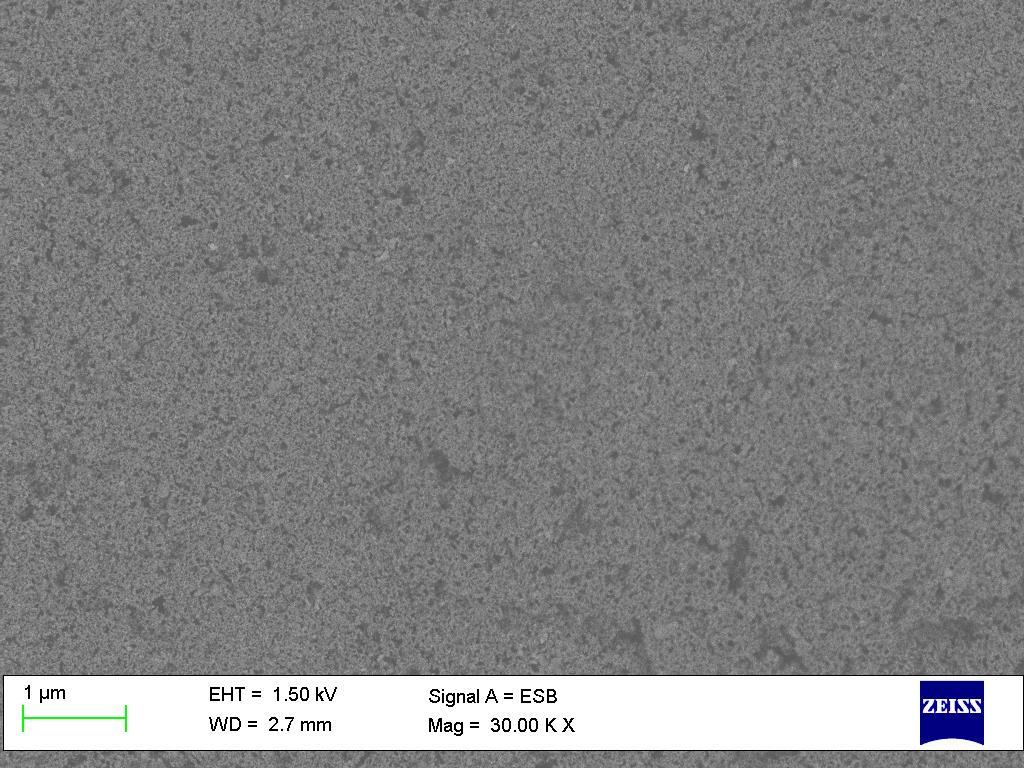


193 a b c d e Figure 6.8. SEM images of the top view on the mp-tio2 thin films of (a) un-treated, (b) furnace-sintered at 450oC for 30 min; and laser-sintered at constant power density of 85 W/cm2 for irradiation of 1 minutes with variation of duty cycles of 75 ms/25 ms (c), 100 ms/25 ms (d) and 125 ms/25 ms(e), red scale bar (100 nm). 193
194 6.4.3 Cross sectional view of TiO 2 -BLs and mesoporous thin films Mesoporous TiO 2 thin films: Figure 6.9 shows cross sectional SEM images of the mesoporous TiO 2 films treated under different conditions. Thickness of the un-treated TiO 2 film (Figure 6.9a) was 10.5 μm. The one-step and two-step furnace-sintered TiO 2 films (Figures 6.9 b and c) are crack-free with no distortion and had average thickness of 9.7 μm and 9.6 μm respectively. The reduction in the film thickness was attributed to the evaporation of the organic binders and the interconnection of the TiO 2 nanoparticles which resulted in shrinkage of the films under thermal treatment [116,203]. All the films sintered by the laser at the power density of 85 W/cm 2 with variation of duty cycles were crackfree with good adhesion between the compact TiO 2 films and the ITO-glass substrates, as well as between the mp-tio 2 films and the compact TiO 2 layers. The thicknesses of the laser-sintered films at the duty cycle 75ms/25ms (Figure 6.3d), 100ms/25ms (Figure 6.9e) and 125ms/25ms (Figure 6.9f) were 9.8 μm, 9.6 μm and 9.3 μm respectively. This suggested that the thickness of the films decreased with the increase in laser duty cycle. This was due to the prolonged laser pulses leading to higher temperatures and the time periods available at the temperatures which resulted in formation of denser TiO 2 films. However, the thickness of the film sintered at the duty cycle of 75ms/25ms was still about 2% thicker than that the furnacesintered TiO 2 film. This indicated that the interconnection of the TiO 2 nanoparticles is less efficient. 194

; and Laser- sintered at constant 85 W/cm 2 at duty cycle of 75 ms/25 ms(d), 100 ms/25 ms (e) and 125 ms/25 ms (f). Compact TiO 2 Blocking layers: Figure 6.")
195 Mesoporous TiO2 film Mesoporous TiO2 film ITO layer TCO glass substrate a ITO layer TCO glass substrate b Mesoporous TiO2 film Mesoporous TiO2 film ITO layer TCO glass substrate c ITO layer TCO glass substrate d Mesoporous TiO2 film Mesoporous TiO2 film ITO layer TCO glass substrate ITO layer TCO glass substrate e f Figure 6.9. FEG-SEM images of cross sectional view of the TiO 2 thin films of untreated (a), one-step furnace-sintered at 450 o C for 30 minutes (b), two-step furnace sintered at 450 o C for 30 min.(c); and Laser- sintered at constant 85 W/cm 2 at duty cycle of 75 ms/25 ms(d), 100 ms/25 ms (e) and 125 ms/25 ms (f). Compact TiO 2 Blocking layers: Figure 6.10 shows high magnification cross-sectional SEM images of the compact TiO 2 layers and mesoporous TiO 2 films treated under different conditions. The crosssectional SEM images of all the films consisted of three layers which were the 195
196 mesoporous TiO 2, the compact TiO 2 and the ITO coated glass substrate. The nanostructured compact layers were completely different from the mesoporous TiO 2 film. From Figure 6.10, it can be seen that the TiO 2 compact layers had good conformal coverage to the ITO layers in all the films. For the un-treated TiO 2 precursor layer (Figure 6.10a), the TiO 2 nanoparticles in the TiO 2 film were discrete, and the TiO 2 precursor layer had a thickness of 60 nm. For the one-step furnace treatment (Figure 6.10b), the morphology of the TiO 2 compact layer was like necking of the nanoparticles together, implying crystallisation of the TiO 2 precursor layers. The thickness of the compact TiO 2 layer became 50 nm due to the shrinkage of the layer during the heat treatment. The two-step furnace (figure 6.10c) treatment of the amorphous TiO 2 layer, clearly shows the compact layer with a thickness of 40 nm without holes and in a good adhesion with the mesoporous film. It is believed that a good adhesion between the mesoporous film and the compact layer plays an important role in the enhancement in conductivity and promotes charge collection efficiency in the DSSCs devices [219,220]. Where the structure of the block layer can represent a good tunnel for the electron transfer from the porous film to the ITO substrate. Consequently, it would increase the number of effective electrons pathway with shortening the distance [219]. For the compact layer treated by laser at the duty cycle of 75 ms/25 ms (Figure 6.10d), shows a clear sign of the crystallization and the thickness of the compact layer was reduced from 60 nm to 50 nm. With further increase in the duty cycle to 100 ms/25 ms (Figure 6.10e), the thickness of the compact TiO 2 layer was further reduced to about 40 nm with a crystallinity of the nanoparticles. The compact layer treated at the duty cycle of 125 ms/25 ms (Figure 6.10f), shows a dense layer with a thickness of 40 nm, which was the same as the thickness reached by the duty cycle of 100 ms/25 ms, although the temperature achieved by the duty cycle of 125 ms/25 ms was higher than that of the 100 ms/25 ms, as shown in Figure 6.1. No further densification of the compact layer was observed. In addition, the crystallization of the compact TiO 2 layer was as clear as that observed for the furnace treated sample. 196
 un-treated, (b) one-step furnace sintered at 450 o C for 30 min, (c) twostep furnace sintered at 500 o C for 30min, and laser sintered at 85 W/cm 2")

197 Figure Cross-sectional SEM images of the compact and mesoporous TiO 2 layers. (a) un-treated, (b) one-step furnace sintered at 450 o C for 30 min, (c) twostep furnace sintered at 500 o C for 30min, and laser sintered at 85 W/cm 2 with duty cycles of 75 ms/25 ms (d), 100 ms/25 ms (e) and 125 ms/25 ms (f). 6.5 Photovoltaic performance of DSSCs In order to study the photovoltaic performance of the DSSCs assembled with the photoanodes with and without compact TiO 2 layers and treated by furnace and laser, the measurements of J-V curves and EIS data analysis were made and presented as follows. 197