Crystallographic Textures Measurement
|
|
|
- Roderick Hoover
- 5 years ago
- Views:
Transcription

1 Crystallographic Textures Measurement D. V. Subramanya Sarma Department of Metallurgical and Materials Engineering Indian Institute of Technology Madras

2 Macrotexture through pole figures by XRD X-ray diffractometer
3 Macrotexture through pole figures by XRD Monochromatic radiation required for texture analysis
4 Macrotexture through pole figures by XRD

5 Macrotexture through pole figures by XRD
6 Macrotexture through pole figures by XRD Rotation about an axis perpendicular to the sheet surface (angle ) Rotation about an orthogonal axis (this axis lies in the plane of incident and diffracted beam and is perpendicular to plane normal) by an angle
7 Macrotexture through pole figures by XRD

8 Macrotexture through pole figures by XRD

9 Macrotexture through pole figures by XRD Pole figure scanning
10 Macrotexture through pole figures by XRD Iso-intensity contours in experimental pole figures
11 Macrotexture through pole figures by XRD

12 Macrotexture through pole figures by XRD

13 Defocusing
14 Defocusing
15 Defocusing
16 Defocusing
17 Corrections to pole figure data Background correction: Background error comes because of (1) Fluorescence in the sample, (2) Non-coherent scattering in the sample, (3) Scattering in the path of X-rays by air, (4) Imperfect monochromatic radiation. For a pole figure, the background intensity changes with the tilt angle α, but usually this does not depend on the sample rotation angle β. In practice, the background intensity IBG (α) is measured from pole figure data obtained at an angle away from the diffraction peak angle θ and integrating over β
18 Corrections to pole figure data
19 Defocusing error: Measurement of textures Corrections to pole figure data To correct for this defocusing error, a correction function U(α) must be applied, which for any value of α normalizes the intensity of a random sample to the values at α = 0 :
20 In the case of very thin samples (thin fi lms), however, the volume increase is dominating and an absorption correction becomes necessary. Measurement of textures Corrections to pole figure data Absorption correction: Important in transmission geometry for very thin samples. When a sample analyzed in transmission geometry is tilted, the path length of the x-rays within the sample increases much more than the increase in the diffracting volume, resulting in a strong decrease in diffracted intensity. In the case of reflection of x-rays at an infinitely thick sample, the increase in absorption is exactly balanced by the increase in diffracting volume, such that the reflected integrated intensity remains constant and a special correction is not necessary.
21 Corrections to pole figure data
22 Normalisation: Measurement of textures Corrections to pole figure data After pole figure measurement and subsequent correction of the data with respect to background intensity, defocusing error, and, if necessary, absorption, the pole figure data are available as number of counts, or counts per second, per pole figure point (α,β). For representation of the pole figures and for a subsequent evaluation, however, it is necessary to normalize the intensities to standard units that are not dependent on the experimental parameters. The commonly used convention is to express the data in mrd (multiples of random). where

23 Microtexture in SEM / TEM Electrons SEM-based TEM-based Kossel ECP EBSD SADP Kikuchi
24 Microtexture in TEM Analysis of selected area diffraction (SAD) spot patterns Micro-diffraction and Convergent Beam Electron Diffraction High-resolution electron microscopy (HREM) SAD has been widely used to analyze orientations in a TEM In contrast to other techniques that yield only orientations of individual crystals, SAD also offers the possibility to measure directly pole figures of small volumes in the TEM
25 Microtexture in TEM For the determination of individual orientations, Kikuchi patterns, which are obtained by microdiffraction If highest spatial resolution is required, convergent beam electron diffraction (CBED), is much better suited, as this method combines highest spatial and angular resolutions Preparation of specimens for TEM examination involves electropolishing for metallic materials and other procedures such as ion beam milling for non-metallic materials The standard methods used to prepare electron-transparent (i.e., less than approximately 200 nm thick) specimens that are representative of the bulk material are quite exacting, but they are well established
26 Microtexture in TEM High-Resolution Electron Microscopy A fascinating technique for determination of local orientations in the very smallest volumes. The positions of atoms (more precisely, columns of atoms) are imaged by means of an interference method, which enables one to draw directly conclusions on the crystallographic features. HREM is best suited for determination of mis-orientations as well as for investigation of grain or phase boundaries.

27 Microtexture in TEM HREM photograph of a 17 / 100 grain boundary in gold in which the interfacial structure can be resolved
28 Microtexture in TEM For routine orientation measurement, however, HREM is not appropriate for the following reasons: Sample preparation is very difficult because HREM requires extremely thin samples (~20 nm). Using such thin samples raises the question of whether the orientations determined are actually representative for the sample volume of interest. Interpretation of the results is complicated and requires the use of computer simulations.
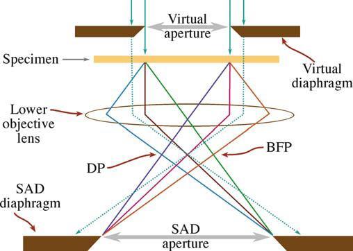
29 Microtexture in TEM To utilize diffraction of electrons at the crystal lattice for orientation determination, the volume of interest is irradiated with a parallel electron beam To achieve a high resolution, the transmitted volume must be very thin (of the order of the mean free path of the electrons in the material), so that multiple diffraction effects are avoided For analysis of small sampled regions, the area of view is reduced by inserting an appropriate aperture in the plane of the first magnified image that has a magnification of typically 25
30 Microtexture in TEM
31 Microtexture in TEM Investigation of diffraction from single-crystal volumes yields characteristic patterns that are composed of a regular arrangement of individual diffraction spots, which can be evaluated for orientation determination SAD pattern of an aluminum crystal with a zone axis near 110
32 Microtexture in TEM The diffraction spots are formed by coherent elastic scattering of the electrons at the crystal lattice. Because of the very short wavelength of the electron radiation, the diffraction angles between the reflecting lattice planes and the primary beam are very small as well at the most approximately 2. This means that all the reflecting planes are situated almost parallel to the primary beam or, in other words, the primary beam is a zone axis of the reflecting planes
33 Microtexture in TEM
 SAD diffraction pattern of evaporated Al with random texture.")
34 Microtexture in TEM Schematic illustration of formation of SAD ring patterns in polycrystalline assemblies. (b) SAD diffraction pattern of evaporated Al with random texture. (c) SAD diffraction pattern of cold-rolled aluminum with strong texture.
35 Microtexture in TEM Formation of SAD pole figures in a TEM; (b) and (c) coverage of the pole figure as the angle α is gradually increased.
")
36 Microtexture in TEM Indexing RD TD Orientation: (101) <1-1-1>

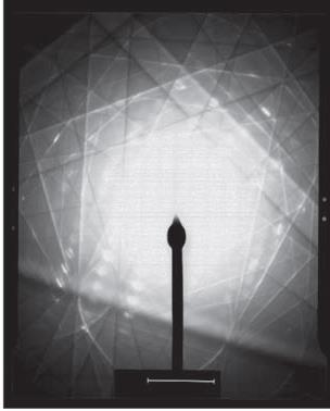
37 Kikuchi lines in TEM
![Kikuchi lines in TEM Simulated diffraction patterns for a [100] axis showing both SAD spots and Kikuchi lines for (a) un-tilted, that is, exact [100] orientation and (b) 2](/docs-images/90/103082065/images/38-0.jpg "tilted orientation. These patterns show that Kikuchi lines have much greater sensitivity to crystal orientation than SAD spots (simulation program TOCA by Zaefferer, 2002).")
38 Kikuchi lines in TEM Simulated diffraction patterns for a [100] axis showing both SAD spots and Kikuchi lines for (a) un-tilted, that is, exact [100] orientation and (b) 2 tilted orientation. These patterns show that Kikuchi lines have much greater sensitivity to crystal orientation than SAD spots (simulation program TOCA by Zaefferer, 2002).
![Kikuchi lines in TEM Micro-diffraction patterns from [111]-oriented crystals obtained with increasing](/docs-images/90/103082065/images/39-2.jpg "convergence of the electron beam.")
39 Kikuchi lines in TEM Micro-diffraction patterns from [111]-oriented crystals obtained with increasing convergence of the electron beam. (a) Kikuchi lines and HOLZ lines in the zero-order Laue zone (ZOLZ) (Nimonic PE16).
40 Kikuchi lines in TEM B p AC = 3.8 cm BC = 2.2 cm AB = 2.65 cm OA = 2.5 cm OB = 1.35 cm OC = 2.7 cm O p A C p 1 d 1 = p 2 d 2 = p 3 d 3 = constant 113 p 3
41 Kikuchi lines in TEM


42 Kikuchi lines in SEM Zone axis
43 Kikuchi lines in SEM

44 The origin of the gnomonic projection, labeled N referred to as the pattern center, PC The radius of the reference sphere, labeled ON and referred to as the specimen-to-screen distance, Z SSD
45 Automatic indexing in EBSD Diffraction pattern capture, digitization Average n frames (1 n 16) Background subtraction Hough transformation (lines points) Evaluate angles between zones Compare sets of known interzonal angles with measured set Select best fit Calculate Euler angles

46 Hough Transform


47 Automatic indexing in EBSD Measurement of textures
48 Automatic Indexing Automated indexing of the Kikuchi patterns is accomplished by making lists of inter-zonal angles, i.e. the angle between each pair of (strong) bands. These angles must correspond to the fixed angles between zones in the crystal structure known to be present in the specimen, e.g. the angle between [001] and [111] is Once the zones have been identified, the geometry of the system permits the orientation of the crystal to be related to that of the pattern.

49 Automatic Indexing x 1,y 1,l l x 3,y 3,l x 2,y 2,l x 4,y 4,l The unit vector n 1 = r 1 x r 2 / r 1 x r 2 is perpendicular to the crystal plane generating the first Kikuchi band and the vector n 2 = r 3 x r 4 / r 3 x r 4 is perpendicular to the crystal plane generating the second Kikuchi band The angle between the planes forming the two Kikuchi bands is cos -1 (n 1 n 2 )

50 Indexing of the planes and zone axis Assigning the orientation / calculation of Euler angles

51 Pattern Centre Calibration Crystal of known orientation, Si [001]
52 Pattern Centre Calibration Iterative Pattern Fitting Calibration via iterative pattern fitting requires only an EBSD pattern of reasonable quality in which at least three bands or zone axes can be identified Equation 1 can then be formulated n(n 1)/2 times, where n is the number of identified zone axes, substituting in the known indices of two of the poles in turn. These equations have to be solved numerically to obtain x PC, y PC, and Z SSD The numerical method needs a first guess for the values of the PC coordinates and Z SSD. If the fi rst guess is reasonably good, less iterations will be required to converge toward the right solution
53 Resolution and Operational Parameters Microscope parameters (SEM / FEGSEM) Material (atomic number) Specimen/microscope geometry (working distance, tilt angle) Accelerating voltage (interaction volume) Probe current (pattern quality) Pattern quality (defects in the crystal)
54 Resolution and Operational Parameters Spatial resolution of EBSD in nickel as a function of accelerating voltage
55 Resolution and Operational Parameters (a) The effect of probe current on effective resolution for several aluminum specimens. The minima in the plots are caused by the reduced pattern-solving accuracy at low probe currents. (b) Effective EBSD spatial resolution for various metals in tungsten filament and FEG SEMs. (c) Misorientation measurements between adjacent points on a single-crystal silicon specimen for four different probe currents (in amperes). The highest-probe current provides the most accurate result.
 Original poor-quality EBSD pattern; (b) original highquality EBSD pattern; (c) Fourier spectrum of (a) (IQ = 0.")
56 Pattern Quality Original and Fourier-transformed EBSD patterns with different quality to derive the image quality IQ. (a) Original poor-quality EBSD pattern; (b) original highquality EBSD pattern; (c) Fourier spectrum of (a) (IQ = 0.29); (d) Fourier spectrum of (b) (IQ = 0.43).
57 Sample Preparation for EBSD Specimen preparation is straightforward, often similar to that for optical microscopy. The specimen preparation objective for EBSD can be stated very simply: the top nm of the specimen should be representative of the region from which crystallographic information is sought. The specimen surface must not be obscured in any way by mechanical damage (e.g., grinding), surface layers (e.g., oxides and most coatings), or contamination. The standard metallographic preparation route for most specimens, especially metals and alloys, is mounting, grinding, and polishing
 No coating, 40 kv accelerating voltage; (b) no coating, 10 kv accelerating voltage; (c) coating with 5 nm of nickel, 40 kv accelerating voltage; (d) coating with 5 nm nickel, 10 kv accelerating")
58 Sample Preparation for EBSD Illustration of the penetration depth of the electron beam in a silicon EBSD specimen. (a) No coating, 40 kv accelerating voltage; (b) no coating, 10 kv accelerating voltage; (c) coating with 5 nm of nickel, 40 kv accelerating voltage; (d) coating with 5 nm nickel, 10 kv accelerating voltage. There is less beam penetration at 10 kv since the underlying silicon pattern is indistinct
59 Sample Preparation for EBSD Mounting the specimens in a conducting medium is clearly advantageous for SEM work; otherwise, electrical contact with the specimen can be established by using silver or carbon paint or conductive tape, or simply by cutting the specimen from the mount after the preliminary preparation stages. It is the final preparation step that ensures suitability for EBSD. Diamond polishing is not an appropriate final stage because of the remnant mechanical damage entailed. A highly recommended method for preparing a variety of specimens for EBSD is final polishing in colloidal silica, since this medium does not introduce the harsh mechanical damage associated with diamond polishing
.")
60 Pattern Quality map EBSD map of hot-deformed and partly recrystallized Al Mg alloy (AA5182). (a) Pattern quality map in which the high quality patterns appear brighter


61 Orientation mapping Grains of the main texture components coloured Red=Cube {100}001, Green=Goss {011}100, Blue=Brass {011}211


62 Strongly cube textured material i.e., strong {100} <001> orientation Measurement of textures Orientation mapping 100 pole figure

63 Mesotexture analysis Analysis of grain boundary network and the misorientation distribution permits quantitative description of microstructure