Materials-by-Design gets Serious!
|
|
|
- Erin Montgomery
- 5 years ago
- Views:
Transcription

1 Materials-by-Design gets Serious! New $25 Million National User Facility dedicated to Electronic Materials by Design!


2 Bulk User Facilities Thin Film Theory & Computation New Chemistry New Physics New Materials Science New Materials Electron Microscopy Characterization k y (π/a) k x (π/a)


")

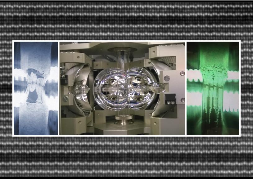
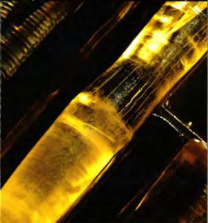
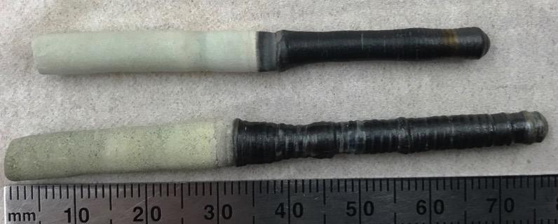
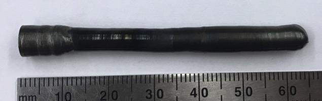
3 Bulk Crystal Growth User Facility Expanded Growth Condi1ons, in situ Growth Guidance Vapor Equilibria Machine Learning Safe highly toxics, Bridgeman in FZ P = 300 atm (first in world) Supercri8cal fluids Laser-heated floating zone Tyrel McQueen


")


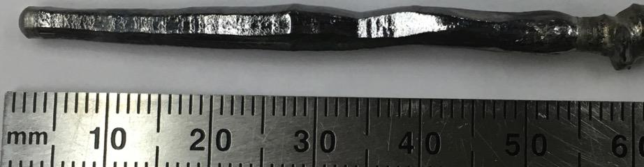
4 Bulk Crystal Growth User Facility (111) crystal


 via MOCVD")


5 Thin Film User Facility (opens 2018) Expanded Growth Condi1ons MBE of any 11 of 62 elements at one 8me (and refills without breaking chamber vacuum) T sub < 1000 C Many others (e.g., chalcogenides) via MOCVD Rou1ne, in situ Growth and Characteriza1on MOCVD of 1 ML thick MoS 2, MoSe 2, WS 2, WSe 2 over 4 wafers (Kang et al. Nature Nature 2017) Jiwoong Park


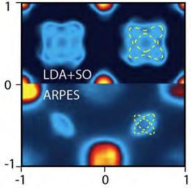
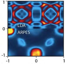
6 Oxide MBE + ARPES Angle-Resolved Photoemission Spectroscopy (Kyle Shen)


7 MBE + ARPES + MOCVD Titanates SrTiO 3 Sr 2 TiO 4 LaTiO 3 Vanadates SrVO 3 LaVO 3 SrVO 3 / LaVO 3 Manganites La 1-x Sr x MnO 3 SrMnO 3 amno 3 / SrMnO 3 Nickelates LaNiO 3 Cuprates La 2 CuO 4 T Sr 1-x La x CuO 2 Ruthenates RuO 2 SrRuO 3 Sr 2 RuO 4 BaRuO 3 Ba 2 RuO 4 CaRuO 3 Ca 2 RuO 4 Pb 2 Ru 2 O 6.5 Iridates IrO 2 IrO 2 / TiO 2 SrIrO 3 Sr 2 IrO 4 Ba 2 IrO 4 Bi 2 Ir 2 O 7 Other Materials YbAl 3 LuAl 3 YbAl 3 / LuAl 3 BaBiO 3 BaSnO 3 BaPbO 3 FeSe


8 Thin Film User Facility (opens 2018) MBE + ARPES + MOCVD Lab Stand- Alone MOCVD Lab


 389 2")
 11682")

9 Electron Microscopy User Facility FEI T12 TEM FEI F20 monochromated S/TEM Probe corrected Nion UltraSTEM First 5 th order aberration corrected STEM Probe Corrected FEI Titan Themis cryostem First of its kind cryostem Imaging grains in 2D materials Atomic resolution Imaging Atomic resolution Elemental Mapping - Atomic resolution imaging + spectroscopic mapping at LN 2 temp. - Magnetic imaging by Lorentz TEM Park, McEuen, Muller, Nature 469 (2011) nm Kourkoutis, Song, Hwang, Muller, PNAS 107 (2010) Muller, Kourkoutis, Murfitt, Song, Hwang, Silcox, Dellby, Krivanek, Science 319 (2008) 1073 Lena Kourkoutis
 Records every")

 Diffraction pattern in")


10 Electron Microscope Pixel Array Detector (EMPAD) Records every electron that passes through the sample, at every probe position! Single Electron Sensitivity (noise is 1/50 e ) Diffraction pattern in 1 ms e - Dynamic Range > 1,000,000:1 # e Lattice constant map (Å) 500 nm WS 2 WSe 2 Uniaxial strain map % High Speed: 0.86 ms/frame 5 nm SiN x Relaxed Relaxed 0 Monolayer WS 2 -WSe 2 multijunctions 500 nm M.W. Tate et al. Microsc. & Microanal. 22, 237 (2016) Strained 1%


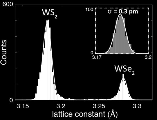
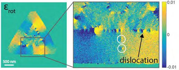
11 Lattice & Strain Mapping of Monolayers with Sub-pm Precision Histogram


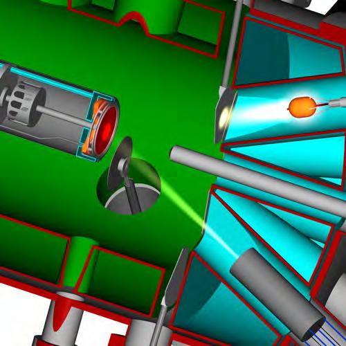
12 Ptychography for Low-Dose, Super-Resolution Imaging Electron beam lenses Diffraction from an atomic-sized beam contains phase information in the overlapping beams. Our EMPAD detector is sensitive enough to measure higher order beams thus increasing spatial resolution beyond the limitations of the lens MoS 2 Diffraction sample Central beam EMPAD Diffracted Beams


13 Examples of Super-Resolution Imaging with Pytchography MoS 2 at 80 kev ADF Ptychography 3Å 4α Nb 3 Cl 8 at 120 kev ADF Ptychography Sulfur monovacancy Nb Cl 0.67 Å 2α 0.98 Å 5α 0.39 Å Super high resolution makes it easier to see defects

14 Theory User Facility Helping to close the gap with experiment Two modes of opera8on Consulta8on Advise and Help Collabora8on coauthoring Key elements: Fundamental theory Well-known Algorithms Software packages Efficiency techniques Aided by: Materials-by-Design Toolbox Community On-Line Short Courses Open-source code Databases Tutorials Written instructions Key elements: Advanced/new theory Advanced/new Algorithms Specialty Software packages Runtime optimization Aided by: Materials-by-Design Toolbox Community Databases Commercial codes Specialized codes Code modifications Larry Wang


15 Maximizing Data Availability and Usability Collect Everything, Use everything, Make available everything Machine Learning Sloan Founda8on and JHU All data available online NSF ACI


16 2018 Summer Schools Johns Hopkins: 3 rd Synthesis and Materials Discovery Summer School June Cornell: An Introduc8on to Density Func8onal Theory for Experimentalists July 8-13 PARADIM Summer Schools are FREE to all participants (industry too) Instructor: Feliciano Gius1no Professor of Materials University of Oxford
 floating-zone growth Mass spectrometry during bulk crystal growth Integrated MBE + ARPES + MOCVD")


17 PARADIM A National User Facility Theory to help guide; informed by experiment High-pressure (supercritical fluid) floating-zone growth Mass spectrometry during bulk crystal growth Integrated MBE + ARPES + MOCVD High sensitivity, high dynamic range pixel array detector for quantitative mapping of E and B fields with sub-nm resolution Stable cryo-stages for STEM and STEM-EELS Free to the highest ranked user proposals from U.S.A. academic institutions or national labs All samples produced in PARADIM belong to the user Optimized recipes eventually become public domain PARADIM interns utilize optimized recipes to fulfill sample requests