DEFECTS IN SILICON-GERMANIUM STRAINED EPITAXIAL LAYERS MARK DYNNA. A Thesis. Submitted to the School of Graduate Studies.
|
|
|
- Sara White
- 5 years ago
- Views:
Transcription
1 DEFECTS IN SILICON-GERMANIUM STRAINED EPITAXIAL LAYERS By MARK DYNNA A Thesis Submitted to the School of Graduate Studies in Partial Fulfillment of the Requirements for the Degree Doctor of Philosophy McMaster University (c) Copyright by Mark Dynna, 1993.
2 DEFECTS IN SILICON-GERMANIUM STRAINED EPITAXIAL LAYERS
3 DOCTOR OF PHILOSOPHY (1993) (Materials Science and Engineering) McMASTER UNIVERSITY Hamilton, Ontario TITLE: Defects in Silicon-Germanium Strained Epitaxial Layers AUTHOR: Mark Dynna, B.A.Sc. (University of Toronto) M.A.Sc. (University of Toronto) SUPERVISOR: Professor G.C. Weatherly NUMBER OF PAGES: xiii, 168 (ill
4 Abstract The energies of one and two-dimensional dislocation arrays lying near a free surface are evaluated directly from the stress fields of single dislocations in 3. half-space. These results are used to obtain expressions giving the equilibrium spacings of a number of different arrays relieving misfit in a strained epitaxial system. Numerical calculations are performed for the case of edge and 60 dislocations relieving strain in a silicon-germanium layer deposited on a silicon substrate. This method is also used to calculate the energies of various low angle grain boundaries in a half-space. Single-ended dislocation sources are observed using transmission electron microscopy in two short-period Si-Ge superlattices grown on Si(lOO). Their formation is linked to the development of non-planar layers during the growth of the superlattices. The relaxation of these superlattices takes place at significantly lower temperatures than equivalently strained homogeneous epilayers. Si-Ge short period superlattices deposited on Si(lOO) are shown to rela.\: through twinning on {lll} planes if the deposited layers become grossly non-planar. Twinning is accompanied by the formation of a diamond hexagonal phase. No 60 ~(1l0) dislocations relieving misfit are present in the (iii)
5 strained layer structure. The nature and ongin of a new type of defect in Sit_xGeJSi strained layer structures, the "pagoda" defect, is studied using transmission electron microscopy. The defects are found to propagate in a direction determined by the position of the Si source in unrotated substrates, and to have their origin in the role played by SiC particles (left after cleaning the substrate) during the growth proces3. Pits that form at the SiC particles are preserved during MBE growth and perturb the strained layers, leading to the formation of pagodas. (iv)
6 Acknowledgements The author would like to express thanks to his supervisor, Dr. G.C. Weatherly, for his support and encouragement throughout this work. Thanks are also due to Dr. Z.S. Basinski for helpful discussions. The author would also like to thank Dr. D.C. Houghton and Dr. T.E. Jackman for providing the material used in this study, John McCaffrey for preparing some of the TEM specimens, and Heather Halabourda for assistance with the word processing. The financial support of the Ontario Government and McMaster University is gratefully acknowledged. (v)
7 Table of Contents Abstract Acknowledgements Table of Contents List of Tables List of Figures Chapter 1 Chapter 2 Chapter 3 Introduction Review 2.1 The Growth of Heteroepitaxial Films Systems in which there is Perfect Lattice Matching Systems in which there is Uniform Lattice Mismatch Si-Ge/Si(100) Heteroepitaxy 2.2 Dislocations in Strained Layers Energetics The Nucleation of Dislocations in Sit_xGex Strained Layer Structures Propagation and Multiplication of Dislocations 2.3 Electron Microscopy Dislocation Energetics in a IIalf-5pace (iii) (v) (vi) (viii) (ixl The Energetics of Dislocation Arrays 40 in a Half-Space General Method Dislocation Self Energy Interaction Between Dislocation and 49 Epilayer - The Critical Thickness Analysis of One-Dimensional 52 Dislocation Arrays Two-Dimensional Arrays Computations for Silicon-Germanium 68 Strained Layers Grown on Si(100) (vi)
8 3.2 Energies of Low Angle Grain Boundaries 78 in a Half-Space The Energy of an Array of Edge Dipoles Tilt Boundary Energies Twist Boundary Energies 85 Chapter 4 Chapter 5 Chapter 6 Chapter 7 Chapter 8 Appendix References Experimental Procedure Dislocation Sources in Si-Ge Strained Layer Structures Relaxation Via Twinning in Si--Ge Compressively Strained Layers The Pagoda Defect Summary and Conclusions (vii)
9 List of Tables Table 3.1 Equilibrium spacing of two-dimensional arrays of mixed dislocati.:.ns in the vicinity of the critical thickness. 75 Table 5.1 Effective stresses in (Si"Gen)p short period superlattices and in homogeneous epilayers. 104 (viii)
10 List of Figures Figure 2.1 Schematic representation of the reconstructed 11 Si(100) surface. Figure 2.2 Internally stressed system formed by joining 15 two materials havin~ different lattice parameters. Figure 2.3 One-dimensional array of mixed dislocations 24 having a similar orientation lying parallel to the free surfdce in a semi-infinite solid. Figure 3.1 One-dimensional arrays of mixed dislocations 42 having (a) similar and (b) alternating orientations lying parallel to the free surface in a semi-infinite solid. Figure 3.2 N dislocations of spacing d in a finite epilayer. 54 L = Nd. Figure 3.3 Critical thickness vs. percent Ge for dislocations (solid curve) and 60 dislocations (dashed curve) in the case of Si-Ge deposited on Si(100). Figure 3.4 Dislocation spacing vs. epilayer thickness for 90 dislocations relieving strain in Sio.gGeo.\ 72 deposited on Si(100). The solid curve corresponds to the present work, while the dashed curve represents Matthew's approximation. (ixl
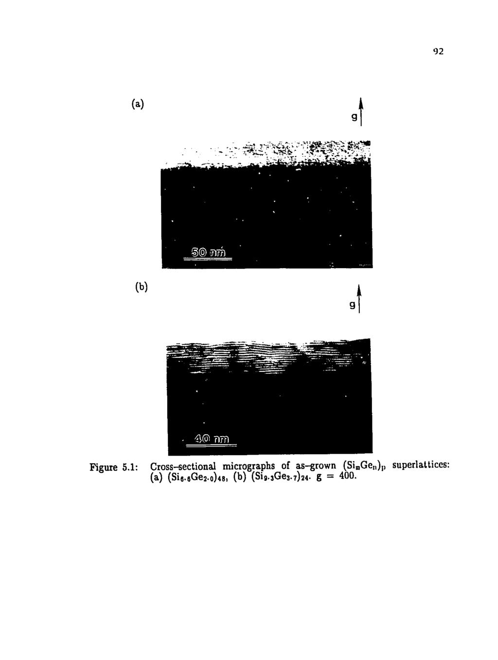
11 Figure 3.5 Dislocation spacing vs. epilayer thickness for 60' dislocations relieving strain in Sio.gGeo.1 deposited on Si(IOO). Lower solid curve: dislocations of simil'!.r orientation whose screw components give rise to a negative interaction energy. Dashed curve: dislocations of alternating orientation. Upper solid curve: dislocations of similar orientation whose screw components give rise to a positive interaction energy. Figure 3.6 Energy at equilibrium spacing vs. epilayer thickness in Sio.gGeo.! deposited on Si(IOO) for 60' dislocations of similar orientation whose screw components ~ve rise to a negative interaction energy (solid curve) and 60' dislocations of alternating orientation (dashed curve). 77 Figure 3.7 Array of edge dislocations forming a tilt boundary lying parallel to the free surface in a semi-infinite solid. 80 Figure 3.8 illustration of a tilt boundary in a serni-infinite fcc/diamond cubic lattice; surface normal = (100). 83 Figure 5.1 Cross-sectional micrographs of as-grown (SimGen)p superlattices. g = Figure 5.2 Dislocation network in (Si g.jgej'7h4 superlattice formed on annealing for 20 s at 500' C. g = 022 weak beam. 93 Figure 5.3 Dislocation source in (Si g.jgej.7h4 superlattice annealed 20 s at 450' C. g = 022 weak beam. 94 Figure 5.4 Dislocation source in (Sig.3Ge3.7h4 superlattice annealed 20 s at 450' C. g = 022 weak beam. 95 Figure 5.5 Dislocation sources in (Sis.sGe2.o)48 superlattice annealed 20 5 at 500' C. g = 022. (x) 97
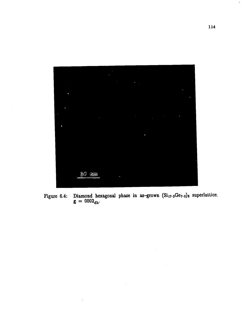
12 Figure 5.6 Dislocation sources in (Si 606Ge2. 0) superlattice annealed 20 s at 500' C. g = 022 dark field. Figure 5.7 Activated dislocation source in (Si606Ge2.0)48 99 superlattice annealed 20 s at 500' C. g = 022. Figure 5.8 Activated dislocation source in (Si 6.6Ge2.0) superlattice annealed 20 s at 500' C. g = 022 weak beam. Figure 5.9 Inactive dislocation source in (Si6-6Ge2.0) superlattice annealed 20 s at 500' C. g = 022. Figure 5.10 Inactive dislocation source in (Si6.6Ge2.0) superlattice annealed 20 s at 500' C. g = 022 weak beam. Figure 5.11 Dislocation configurations relieving stress 106 concentration near a germanium cluster. Figure 6.1 Cross-sectional micrograph of (Sil7.sGe7.o)s 111 superlattice in the as-grown state. g = 400. Figure 6.2 Plan view micrograph of (Sil7.SGe7.0)s 112 superlattice in the as-grown state. g = 022. Figure 6.3 floo] diffraction pattern of as-grown 113 Si 17. ~Ge7'0)s superlattice. Figure 6.4 Diamond hexagonal phase in as-grown 114 (Si17.sGe7.o)s superlattice. g = 0002 dh. Figure 6.5 f411] diffraction pattern of as-grown 115 Si17.sGe7.0)s superlattice. Figure 6.6 {Ill} twins in as-grown (Si 17. SGe7.0)s 117 superlattice. (xi)
13 Figure 6.7 {Ill} twins in (Si17.SGe7.0)s superlattice annealed 20 s at 700' C. 118 Figure 6.8 {1l1} twins in (Si17.SGe7.0)s superlattice annealed 2000 s at 700' C. 119 Figure 6.9 {111} twins in (Si17.SGe7.0)S superlattice annealed 300 s at 800' C. 120 Figure 6.10 Diamond hexagonal phase in (Si17.SGe7.0)s superlattice annealed 200 s at 700' C. g = 0002 dh 121 Figure 6.11 Diamond hexagonal phase in (Si17.sGe7.0)S superlattice annealed 300 s at 800' C. g = 0002 dh 122 Figure 6.12 Cross- ectional micrograph of {Ill} twins in (Si 17.SGe7.0)S superlattice annealed 2000 s at 700' C. g = Figure 6.13 Moire fringes from (Si17.SGe7'0)s superlattice annealed 20 5 at 700' C. g = Figure 6.14 [100] diffraction pattern of (Si17.SGe7.0)s superlattice annealed at 800' C. 126 Figure 6.15 [100] diffraction pattern of (Si17.sGe7.0)s superlattice annealed at 700' C. 127 Figure 6.16 [411] diffraction pattern of (Si17.SGe7.0)s superlattice annealed 20 s at 700' C. 128 Figure 6.17 [411] diffraction pattern of (Si17.sGe7.o)s superlattice annealed at at 700' C. 129 Figure 7.1 Contrast from pagodas in a 20-period SiO.7SGeO.24/Si superlattice, g = 400, 5 ~ O. 133 (xii)
14 Figure 7.2 Chevron contrast from a 20-period 135 Sio'76Geo.24/Si superlattice, g = 022, s N O. Figure 7.3 Contrast from pagodas in a 2o-period 136 Si o.65geo.35 superjattice. g = 400, s ~ 0 - both structure factor and str'l.in field contrast are visible. Figure 7.4 Contrast from pagodas in a 2o-period 137 Sio'65Geo.35 superlattice. g = 400, s>>0 - only structure factor contrast contributes to the image. Figure 7.5 Contrast from pagodas in a 2o-period 139 Sio.65Geo.35 superlattice with g = 133 and 133 equally excited. Figure 7.6 Contrast from pagodas in a 2o-period 140 Sio.65Geo.35 superlattice with g = 133 and 133 equally excited. Complement of figure 7.5. Figure 7.7 Thin region of a 2o-period Sio.65Geo.35/Si 141 superjatticej g = 400, showing bending of strained layers. Figure 7.8 Sio'65Geo.3s/Si superlatticej g = 400, showing the correlation between the position 142 of thin SiC particles at the original substrate, the B-{}oped layer (arrowed), and the pagodas in the first few strain~d layers. Figure 7.9 Diagram illustrating the origin of the contrast 145 inversion found on tilting along the 133 Kikuchi b~d in opposite directions from the [oil] zone axis. Figure 7.10 Diagram illustrating the stages involved in the 147 formation of a depression at the location of a SiC particle in a growing surface. (xiii)
15 CHAPTER 1 Introduction Silicon-germanium heteroepitaxy is a subject of current interest - the growth of strained layer structures in this lattice-mismatched system by techniques such as molecular beam epitaxy or chemical vapour deposition is believed to hold considerable technological promise. Strain-induced modifications of the bandgap make possible the design of electronic and optoelectronic devices which are unobtainable using unstrained silicon. An important example of an electronic device making use of Si-Ge strained layers is the Si-Ge/Si heterojunction bipolar transistor (Patten et al. 1990). Optoelectronic devices include the p-i-n diode (Lang et al. 1985) and the Sil-XGex/Si digital optoelectronic switch (Kovacic et al. 1991). However. the effective manufacture of such devices requires that the strained layers be essentially free of defects such as dislocations. stacking faults. and twins. and therefore an understanding of the relationship between defect formation and the geometrical structure of the device. the conditions under which it is grown. and its subsequent processing treatments is crucial. This thesis examines the formation of defects in various Si-Ge strained layer structures deposited on Si(100). Homogeneous epilayers, Sil_xGex/Si superlattices and short-period (SimGell)p superlattices grown by 1
16
17
18
19
20
21
22
23
24
25
26
27
28
29
30
31
32
33
34
35
36
37
38
39
40
41
42
43
44
45
46
47
48
49
50
51
52
53
54
55
56
57
58
59
60
61
62
63
64
65
66
67
68
69
70
71
72
73
74
75
76
77
78
79
80
81
82
83
84
85
86
87
88
89
90
91
92
93
94
95
96
97
98
99
100
101
102
103
104
105
106
107
108
109
110
111
112
113
114
115
116
117
118
119
120
121
122
123
124
125
126
127
128
129
130
131
132
133
134
135
136
137
138
139
140
141
142
143
144
145
146
147
148
149
150
151
152
153
154
155
156
157
158
159
160
161
162
163
164
165
166
167
168
169
170
171
172
173
174
175
176
177
178
179
180
181
182