FESEM Analysis of BPSG Films After Reflow
|
|
|
- Dennis Owens
- 5 years ago
- Views:
Transcription

1 Chiang Mai J. Sci. 2007; 34(1) 35 Chiang Mai J. Sci. 2007; 34(1) : Contributed Paper FESEM Analysis of BPSG Films After Reflow Uda Hashim*, Nik H.N. Hamat, and Ramzan M. Ayub Micro Fabrication Cleanroom, School of Microelectronic Engineering, Northern Malaysia University College of Engineering, Kuala Perlis, Perlis, Malasia. *Author for correspondence; uda@kukum.edu.my Received: 11 March 2006 Accepted: 11 June ABSTRACT The reflow behavior of BPSG films deposited by plasma enhanced chemical vapor deposition has been studied in several annealing ambient atmospheres. A new recipe for annealing process has been created and performed to improve the planarization for BPSG film after reflow. This improvement is for 0.35µm technology using steam annealing method at different temperatures. Reflow process was carried out by furnace heating. Reflow was studied over the temperature range of 850 C to 900 C. Cross sectional scanning electron microscopy using FESEM has been employed to study the angles of BPSG films slope after images analysis. The samples have been separated into two groups of samples: staining and without staining with HF. The experiments lead to the conclusion that the staining samples with HF provides clearer images for analysis. By using steam annealing method, the better surface planarization of BPSG film has been achieved. Keywords: FEM, BPSG films, reflow process, annealing. 1. INTRODUCTION All multilayer metallization schemes now are almost required some planarization of the dielectric material which is deposited over the poly or metal lines. This planarization is needed because of poor metal step coverage, or to minimize the amount of over etch required for blank metal deposition and etch back processes. The three most widely used processes are BPSG reflow, spin on glass, and photoresist [1]. In this research paper, BPSG reflow has been used. Reflow of dielectric films has been effective to a degree in reducing local variations in topography of multilevel interconnections [2]. As a premetal dielectric, BPSG has been widely used for device planarization. Phosphosilicate-doped silicon dioxide, commonly referred to as phosphosilicate glass (PSG), has been used widely as an interlayer in multilevel metallization. It is an expansively useful as a passivation layer because it inhibits the diffusion of impurities, and it softens and flows at 950 C to 1100 C to create a smooth topography that is useful for depositing metals. PSG films with 4-7 wt% phosphorus concentration require temperature in excess of 1000 C to demonstrate substantial flow. Borophosphosilicate glass (BPSG) reveals a better performance in this respect as it reflows at temperatures below 900 C [3, 4]. BPSG reflow process has been commonly used to obtain insulating films with reasonably flat surfaces. These films exhibit profiles over steps that get progressively
2 36 Chiang Mai J. Sci. 2007; 34(1) smoother with higher phosphorus and boron concentration, reflecting the corresponding enhancement in viscous flow. Post-deposition film reflow can be performed using either conventional furnace or rapid thermal annealing; the reflowed profile depends on annealing temperature as well as ambient gases [5]. In this experiment, reflow process was carried out by furnace heating. A low thermal budget can be maintained using steam anneal. Earlier studies from Thakur et al. [6] revealed that a BPSG thermal budget can be reduced through both steam annealing and rapid thermal processing. The effect of annealing ambient reveals that using steam yields the best reflow [5]. The purpose of this experiment is to improve the planarization of BPSG film for 0.35 µm technology after reflow by using steam annealing method. Steam annealing method was done at different temperatures. 2. EXPERIMENTS The topography substrates understudy were fabricated on <100> oriented P-type silicon wafers with resistivity of cm. Six wafers were used in this experiments. In this experiment, the angles of the BPSG films slope were the response observed after annealing process. The angles must be as low as possible in order to get a good topography of the BPSG films. The thickness of the BPSG film is 3500Å while the uniformity has to be maintained as low as 5%. The Boron and Phosphorus contents of the BPSG layer are 4.7% and 5.3% respectively. A new recipe was created and performed for annealing process using diffusion furnace system. This new recipe used steam annealing at 850 C and 900 C while there was only nitrogen gas used for current annealing recipe during the reflow process. A standard 0.35µ m CMOS technology is utilized. Six wafers are following accordingly to the 0.35µm CMOS process sequences until reached the BPSG deposition steps whereby the experiment is begun. These wafers were marked as number 1 until 6. All wafers were loaded into PECVD Table 1. BPSG reflow process at different conditions. Wafer Number Recipes for BPSG annealing 1 Pre annealing 2 N 2 annealing at 850 o C 3 steam annealing at 850 o C 4 steam annealing at 850 o C 5 steam annealing at 900 o C 6 steam annealing at 900 o C chamber to deposit BPSG film for 3500Å thickness. Details of the PECVD system design and process conditions used in depositing the BPSG films are discussed elsewhere [7-8]. The first wafer was used for pre annealing process while the rest proceeded to the next step. After BPSG film deposition, they were flowed in furnace. The samples were split into several conditions for reflowing the BPSG films in furnace after have gone through the scrubbing process. Four conditions of reflow process are compared and illustrated in Table 1. The steam generated by the pyrogenic combustion of hydrogen and oxygen was readily available in anneal furnace. In this process, the wafers were separated for three different annealing process recipes. Wafer number 2 annealed in nitrogen gas for current BPSG annealing process at 850 C. Wafers number 3 and 4 were used steam annealing process at temperature of 850 C and as 900 C for wafers number 5 and 6. Each wafer was run individually in order to get repeatable results. The process flow is shown in Figure 1.
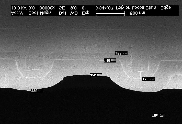
3 Chiang Mai J. Sci. 2007; 34(1) 37 Figure 1. Simple process flow for BPSG flow and reflow conditions. The wafers were finally sent to the Failure Analysis Laboratory for physical analysis of BPSG film topography cross section view using Field Emission Scanning Electron Microscope (FESEM). The FESEM provides a high current density into a small spot size [5]. The analysis of the images has been done locally at the edge and the center of the wafers. The wafers were cut into two for analyzing the effect of HF staining and without HF staining. For staining effect analyzing, the wafers were cleaved, polished and stained with HF before physical crosssectional analysis using FESEM. For each area, two micrograph photos were taken at active and. Based on the photos, the angles of the BPSG films slope were measured. 3. RESULTS AND DISCUSSION For each experimental run, the crosssections of the film profiles were taken with FESEM. The after-reflow angles were also measured. Figure 2 shows how the afterreflow angle is measured. Figure 2. Measurement of an after-reflow angle.


4 38 Chiang Mai J. Sci. 2007; 34(1) Figure 3. FESEM micrograph of BPSG for wafer number 1 at edge area. Figure 4. FESEM micrograph of BPSG for wafer number 1 at the center area. Figure 3 shows the topography taken at the edge area of the wafer for active and. The angles of BPSG film slopes are 73º for active area and 72º for LOCOS area. These images are for the samples underwent the pre-annealing process. Figure 4 illustrates the topography taken at the active and for the center of the wafer for the same conditions. The angles for these slopes are 70º and 76º. It is clearly seen that the sample is not well planarized.


5 Chiang Mai J. Sci. 2007; 34(1) 39 Figure 5. FESEM analysis for wafer number 1 at edge area without staining with HF. Figure 6. FESEM micrograph for wafer number 1 at center area without staining with HF. Figures 5 and 6 indicates the images taken at active and at the edge and the center of the wafer number 1 without underwent the staining with HF process. The images are not very clear compared to the images of the staining wafer for FESEM analysis in Figures 3 and 4. The angles of the BPSG film slopes are 59º, 49º, 60º and 64º. These angles are smaller than the angles obtained from the staining sample.
 Figure 7.")


6 40 Chiang Mai J. Sci. 2007; 34(1) Figure 7. FESEM cross section of BPSG for wafer number 2 at edge area. Figure 8. FESEM cross section of BPSG for wafer number 2 at center area.

7 Chiang Mai J. Sci. 2007; 34(1) 41 Figure 9. FESEM cross section of BPSG for wafer number 2 at edge area without staining with HF. Figure 10. FESEM micrograph of BPSG at center area for wafer number 2 without HF staining. Illustrated images in Figures 7, 8, 9 and 10 are for the wafer that has gone through the current annealing process with nitrogen gas during reflow process at 850ºC. According to the literature, the use of nitrogen anneals in reflow studies of BPSG result in superior reflow properties. The slopes of BPSG film for this wafer produced the angles of 21º, 50º, 49º, 65º, 40º, 53º, 31º and 58º. The angles of slopes extracted from the images of wafer number 1 and 2 are quite bigger. This means the BPSG film was not planarized well. The HF staining samples are shown clear images for analysis. Then, the experiment has been created using steam annealing method in order to improve the planarization of BPSG film. This experiment has been performed at temperatures of 850ºC and 900ºC. Steam often used in PSG and BPSG flow, was the next choice for anneals, although there was no reason to expect that the composition of the films would be altered following steam anneals, since compositional change appeared to be associated with the presence of H 2.


8 42 Chiang Mai J. Sci. 2007; 34(1) Figure 11. FESEM micrograph of BPSG at edge area for wafer number 3. Figure 12. FESEM micrograph of BPSG at center area for wafer number 3.


9 Chiang Mai J. Sci. 2007; 34(1) 43 Figure 13. FESEM micrograph at edge area for wafer number 3 without HF staining. Figure 14. FESEM micrograph at center area for wafer number 3 without HF staining. Figures 11, 12, 13 and 14 show the images of the wafer underwent steam annealing method at 850ºC at both active and LOCOS area for the edge and center of wafer number 3. The angles obtained for this wafer are 24º, 19º, 27º, and 42º for stained sample and 14º, 20º, 22º and 20º for without HF stained sample. These angles indicate better surface planarization of BPSG film has been obtained.


10 44 Chiang Mai J. Sci. 2007; 34(1) Figure 15. FESEM cross section at edge area for wafer number 6. Figure 16. FESEM cross section at the center area for wafer number 6. Figures 15 and 16 illustrate FESEM topography of wafer number 6 at active and for the edge and center area. The BPSG slope angles of these images are 7º, 7º, 6º and 9º. This wafer was gone through the steam annealing process at 900ºC.


11 Chiang Mai J. Sci. 2007; 34(1) 45 Figure 17. FESEM micrograph at edge area of wafer number 6 without HF staining. Figure 18. FESEM micrograph at the center area of wafer number 6 without HF staining. Figures 17 and 18 are the images of the wafer number 6 without HF staining at the edge and center area. This wafer used steam annealing process at 900ºC. The produced angles of BPSG for this condition are 6º, 7º, 7º and 9º respectively for each image. This temperature produced the smallest angles among the others. Steam annealing at 900ºC provides BPSG surface that almost planarized.
12 46 Chiang Mai J. Sci. 2007; 34(1) 4. CONCLUSIONS From the experiment, we concluded that by using steam annealing method at 900 C during reflow process produces better surface planarization of BPSG compared to conventional method and current annealing method using nitrogen gas. The angles obtained from steam annealing method at 900 C are less than 11 that indicate the BPSG surface is almost planarized. The results also show that the samples stained with HF are clearer for FESEM analysis contrast with without HF staining samples. This steam annealing process is proven such a promising method to improve the planarization of BPSG film after reflow. The effect of annealing ambient reveals that using steam annealing yields the best reflow for planarization. REFERENCES [1] Marks J., Law K., and Wang D., In Situ Planarization of Dielectric Surfaces Using Boron Oxide VMIC Conference 1989; [2] Simpson D.L., Croswell R.T., Reisman A., Temple D., and Williams C.K., Planarization Processes and Applications: I Undoped GeO 2 - SiO 2 Glasses, J. Electrochem. Soc., 1999; 146 (10): [3] French P.J., and Wolffenbuttel R.F., Reflow of BPSG For Sensor Applications, J. Micromac. Microeng. 1993; 3: [4] Oberemerok O., and Lytvyn P., Borophos-phosilicate Glass Component Analysis Using Secondary Neutral Mass Spectro-metry, Semiconductor Physics, Quantum Electronics & Optoelectronics 2000; 5: [5] Xia L.Q., Conti R., Galiano M., Campana F., Chandran S., Cote D., Restino D., and Yieh E., High aspect Trench Filling Using Two-Step Subat-mospheric Chemical Vapor Deposited Borophospholicate Glass for 0.18 µm Device Application, J. Electrochem. Soc., 1999; 146 (5): [6] Thakur R.P.S., Gonzalez F., Hawthorne R., Ward V., and Jeng N., Material Research Society Symposium Proceeding, 1993; 303: 283. [7] Hashim U., and Ayub R.M., Field Emission Scanning Electron Microscopy Analysis of Metal Step Coverage Improvement by Reflow, Journal of the Institute of Materials Malaysia, 2004; 5(2), : [8] Banerjee I., Tracy B., Davies P., and McDonald B., Use of Advanced Analytical Techniques for VLSI Failure Analysis, Proceeding of IEEE, 1990;