Silicon Wet Etching. Lecture 21, 22: Dong-il Dan Cho. School of Electrical Engineering and Computer Science, Seoul
|
|
|
- Gwen Watts
- 5 years ago
- Views:
Transcription
1 Lecture 21, 22: Silicon Wet Etching School of Electrical Engineering and Computer Science, Seoul National University Nano/Micro Systems & Controls Laboratory
2 Bulk Micromachining (1) The purpose of bulk micromachining Selectively remove significant amounts of silicon from a substrate Broadly applied in the fabrication of micromachined sensors, actuators, and structures Fabrication method: dry/wet etching Undercut structures that are required to physically move Form membranes on one side of a wafer Make a variety of trenches, holes, or other structures usage and possession is in violation of copyright laws 2
3 Bulk Micromachining (2) Comparison of example bulk silicon etchant SF HNA Alkali-OH EDP TMAH XeF 6 2 plasma DRIE Etch type wet wet wet wet dry dry dry Anisotropy no yes yes yes no varies yes Si etch rate (µm /min) 1 to 3 1 to to to 3 1 >1 Si roughness low low low Variable highh variable low Nitride etch low low low 1 to 10 nm/min - low low Oxide etch (nm/min) 10 to 30 1 to 10 1 to 80 1 low low low P ++ etch stop no yes yes yes no no no CMOS Compatibility no no yes yes yes yes yes Ref.) K. R. Williams, and R. S. Muller, JMEMS, Vol. 5, No. 4, pp , 1996 Marc J. Madou, Fundamentals of MICROFABICATION, 2nd edition usage and possession is in violation of copyright laws 3

 planes) over time Example of anisotropic wet etching: optical bench using")
 E. Kim, MEMS '99, pp.")
4 Isotropic & Anisotropic Etch Isotropic wet etching Etching with chemical reaction etching in all directions Anisotropic wet etching Anisotropic etchants etch much faster in one direction than in another exposing the slowest etching crystal planes ((111) planes) over time Example of anisotropic wet etching: optical bench using (100) silicon (SNU NML) Example of isotropic wet etching: dome shaped diaphragm microphone Ref) E. Kim, MEMS '99, pp , 1999 usage and possession is in violation of copyright laws 4
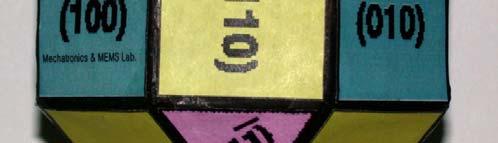
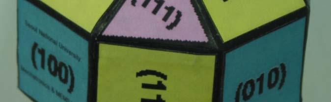
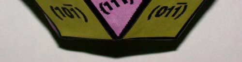
5 Silicon Crystallography (1) z y <111> direction Si crystalline structure Miller indices (i j k) : a specific crystal plane or face {i j k} : a family of equivalent planes [i j k] : a specific direction of a unit vector <i j k> : a family of equivalent directions (111) plane x usage and possession is in violation of copyright laws 5


6 Silicon Crystallography (2) (110) silicon (100) silicon (111) silicon usage and possession is in violation of copyright laws 6
7 Wafer Type (111) PRIMARY FLAT (110) wafer secondary flat is different from company to company usage and possession is in violation of copyright laws 7


8 Isotropic Wet Etching (1) Si isotropic etching by HNA HNA: Hydrofluoric y acid + Nitric acid + Acetic acid Isotropic etchant Si + HNO 3 + 6HF H 2 SiF 6 + HNO 2 + H 2 O + H 2 HNO 3 : oxidize silicon HF: F ion forms the soluble compound, H 2 SiF 6 CH 3 COOH: Prevent dissociation of HNO 3 into NO 3 or NO 2 thereby allowing formation of the species directly responsible for the oxidation of Si: N 2 O 4 2NO 2 Drawback: Poor selectivity over SiO 2 usage and possession is in violation of copyright laws 8
9 Isotropic Wet Etching (2) Electrochemical reaction in HNA etching Injection of holes into Si to form Si 2 + HNO 3 + H 2 O + HNO 2 2HNO 2 + 2OH - + 2h + Si + 2h + Si 2+ Reaction of hydrated Si to form SiO 2 Si OH - Si(OH) 2 SiO 2 + H 2 O Dissolution of SiO 2 and formation of water soluble product SiO 2 + 6HF H 2 SiF 6 + 2H 2 O Overall reaction is, 2e - +HNO +HNO +H +2OH O 2HNO 2 Which can be rewritten, HNO 2 + HNO 3 + H 2 O 2HNO 2 + 2OH - + 2h + Etching is Charge-transfer-driven process usage and possession is in violation of copyright laws 9
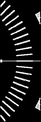
10 Isoetch contours Isotropic Wet Etching (3) usage and possession is in violation of copyright laws 10
11 Region (1) Isotropic Wet Etching (4) For high HF concentrations, contours are parallel to the lines of constant HNO 3, therefore the etch rate is controlled by HNO 3 in this region Leaves little residual oxide Region (2) For high HNO 3 concentrations contours are parallel to the lines of constant HF, therefore the etch rate is controlled by HF in this region Leaves a residual 300~500 nm of oxide Region (3) Initially not very sensitive to the amount of H 2 O, then etch rate falls of sharply for 1:1 HF:HNO 3 ratio usage and possession is in violation of copyright laws 11
12 Isotropic Wet Etching (5) Table of HNA etchant formulations Ref ) Kurt E Ref. E. Petersen Petersen, Proceedings of The IEEE IEEE, 70(5) 70(5), pp pp , 1982 usage and possession is in violation of copyright laws 12
13 Anisotropic Wet Etching (1) Anisotropic wet etching Anisotropic etchants etch much faster in one direction than in another Exposing the slowest etching crystal planes over time (111) planes have the slowest etch rate Several solutions: Alkalic OH (KOH, NaOH), TMAH, EDP Etching at concave corners on (100), stop at (111) intersections, convex corners are under cut usage and possession is in violation of copyright laws 13
14 Anisotropic Wet Etching (2) Examples of anisotropic etching (a) typical pyramidal pit bounded by (111) planes, etched into (100) silicon with an anisotropic etch through a square hole in an oxide mask (b) cantilever mask pattern with a slow convex undercut rate (c) the same mask pattern can result in a substantial degree of undercutting using an etchant with a fast convex undercut rate such as EDP (d) further etching of (c) produces a cantilever beam suspended over pit (e) illustration of the fact that anisotropic etch undercutting converges to predictable shapes after a sufficiently long time usage and possession is in violation of copyright laws 14
15 Anisotropic Wet Etching (3) YAG laser Silicon anisotropic wet etching of (100) and (110) silicon usage and possession is in violation of copyright laws 15

 2 OH Si( OH ) 2e Si( OH ) 4e 4 H O Si( OH ) 2H 2+ 2 2+ 2 + 4 + 2")
 Si Band model of the Si/electrolyte interface")

16 Anisotropic Wet Etching Mechanism (1) H. Seidel et al. Band model of the silicon/electrolyte interface for moderately doped Si 4HO+ 4e 4HO 4H O 4OH 4H 4e 4OH 2H Si + 2 OH Si( OH ) + 2e Si( OH ) 2 OH Si( OH ) 2e Si( OH ) 4e 4 H O Si( OH ) 2H Si OH Si OH 2+ Si Si + 2e - (100) Si Si OH Si OH Si Si + Si Si OH Si Si OH + e - (111) Si Band model of the Si/electrolyte interface (A) p-type Si, (B) n-type Si Si Si Ref.) H. Seidel, et al., J. Electrochem. Soc., vol. 137, no. 11, Nov usage and possession is in violation of copyright laws 16


17 Anisotropic Wet Etching Mechanism (2) M. Elwenspoek et al. Explained the etching mechanism by the crystal growth theory {111} plane has slow etch rate {111} plane is the smooth face {100} plane {110} plane Δμ : the chemical potential difference γ : step free energy h : the height of the step r : the radius of the hole or island ρ : the density of the solid material 2 Δ G = π r hρδ μ+ 2πrγ {111} plane r * γ = hρδμ * * Δ G =Δ G ( r ) = 2 πγ hρδμ Ref.) M. Elwenspoek, and H. V. Jansen, Silicon Micromachining, Cambridge University Press, 1998 usage and possession is in violation of copyright laws 17
18 Si Anisotropic Etchants Alkali-OH EDP(ethylene diamine TMAH (tetramethyl ammonium pyrocatechol) hydroxide) Si etch rate μm /min 1 to 2 1 to 30 ~1 Si roughness Low Low variable 1 Nitride etch Low Low 1to10nm/min 10 Oxide etch 1 to 10 nm/min 1-80 nm/min 1 nm/min Al selective No No 2 Yes 3 Au selective Yes Yes Yes P++ etch stop? Yes Yes Yes Electrochemical stop? Yes Yes Yes CMOS compatible? 4 No Yes Yes Cost 5 Low Moderate Moderate Disposal Easy Difficult Moderate Safety Moderate Low High 1 Varies with wt% TMAH, can be controlled to yield very low roughness. 2 Some formulations do not attack Al, but are not common. 3 With added Si, polysilicic acid or ph control. 4 Defined as 1) allowing wafer to be immersed directly with no special measures and 2) no alkali ions. 5 Includes cost of equipment. usage and possession is in violation of copyright laws 18
19 Hydroxide Etching of Si Several hydroxides are useful KOH, NaOH, CeOH, RbOH, NH 4 OH, TMAH: (CH 3 ) 4 NOH Oxidations of silicon by hydroxyls to form a silicate Si + 2OH - +4h + Si(OH) 2 ++ Reduction of wafer 2H 2 O 4OH - + 2H 2 + 4h + 2O O 2 Silicate further reacts with hydroxyls to form a water soluble complex Si(OH) OH - SiO 2 (OH) H 2 O Overall redox reaction Si + 2OH - + 4H 2 O Si(OH) H 2 + 4OH - usage and possession is in violation of copyright laws 19
20 KOH Etching of Si (1) Typical and most used of the hydroxide etches Etch rate ~1 um/min for (100) Si planes Slow down for boron-doping levels l above 2 x cm -3 ~ 140 nm/hr for silicon nitride ~ 200 nm/min for oxide Anisotropy (111):(110):(100) 1:600:400 usage and possession is in violation of copyright laws 20
21 Simple hardware Hot plate & stirrer KOH Etching of Si (2) Keep cover or use reflux condenser to keep propanol from evaporating Presence of alkali metal (potassium, K) makes this completely incompatible with MOS or CMOS processing Comparatively safer and non-toxic usage and possession is in violation of copyright laws 21
22 KOH Etching of Si (3) Typical recipe and etch rate of KOH Si etching Formulation Temp o C Etch rate ( μm /min) (100)/(111) Etch ratio Masking films (etch rate) KOH (44 g) Water, isopropanol (100 ml) KOH (50 g) Water, isopropanol (100 ml) : :1 SiO 2 (1.4 nm/min) Si 3 N 4 (negligible) SiO 2 (1.4 nm/min) Si 3 N 4 (negligible) usage and possession is in violation of copyright laws 22
23 TMAH Etching of Si (1) Tetra Methyl Ammonium Hydroxide: (CH 3 ) 4 NOH Etch rate: 0.5 ~ 1.5 um/min Etch rate falls off ten times at cm -3 boron concentration B solid solubility in Si: 2.5 x cm -3 Al etch rate 1 um/min 1 nm/min, when ph 13 ph 12 (for 22 wt% TMAH) MOS/CMOS compatible No alkali metals: Li, Na, K, Used in positive photoresist developers which do not use choline. Does not significantly etch SiO 2 or Al! (Bond wire safe!) Anisotropy: (111):(100) 1:10 to 1:35 usage and possession is in violation of copyright laws 23
24 TMAH Etching of Si (2) Hydroxide etches are generally safe and predictable, but they usually involve an alkali metal which makes them incompatible with MOS or CMOS processing. Ammonium hydroxide (NH 4 OH) is one hydroxide which is free of alkali metal, but it is really ammonia which is dissolved into water. Heating to 90 C for etching will rapidly evaporate the ammonia from solution. Ballasting the ammonium hydroxide with a less volatile organic solves the problem: Tetramethyl ammonium hydroxide: (CH 3 ) 4 NOH Tetraethyl th ammonium hydroxide: (C 2 H 5 ) 4 NOH usage and possession is in violation of copyright laws 24
25 TMAH Etching of Si (3) Selectivity of TMAH etchants Selectivity of TMAH Etchants for Various Dielectrics versus (100) Silicon Selectivity Selectivity (Si-doped, 13.5g/l), Selectivity Dielectric 4 wt% TMAH, 80 o C 4 wt% TMAH, 80 o C 20 wt% TMAH, 95 o C Thermal Silicon 5.3 x 10 Dioxide x x 10 3 Low-Temperature Oxide (LTO) 1.3 x x x 10 3 PECVD Oxide 1.4 x x 10 3 No value given LPCVD Silicon Nitrideid 24.4 x x x 10 3 PECVD Silicon Nitride 9.2 x x x 10 3 usage and possession is in violation of copyright laws 25
26 Ammonium Hydroxide Wet Etching NH 4 OH (ammonium hydroxide) CMOS compatibility Several recipes 9.7 wt% NH 4 OH in H 2 O (110) silicon etch rate: 0.11um/min at 85 ~ 92 1~18 wt% NH 4 OH at 75 (100) max. etch rate: 30 um/h Rough surface Disadvantage Slow etch rate, hillock formation Rapid evaporative losses of ammonia gas (noxious) when heated usage and possession is in violation of copyright laws 26
27 EDP Etching of Si (1) Ethylene Diamine Pyrocatechol Also known as Ethylene y diamine-pyrocatechol Water (EPW) EDP etching is readily masked by SiO 2, Si 3 N 4, Au, Cr, Ag, Cu, and Ta But EDP can etch Al! Anisotropy: (111):(100) 1:35 EDP is very corrosive, very carcinogenic, and never allowed near mainstream electronic microfabrication. 50 times slowing of etch rate for > 7 x cm -3 boron doping usage and possession is in violation of copyright laws 27
28 Typical formulation EDP Etching of Si (2) 1 L ethylene diamine, NH 2-CH 2-CH 2-NH g pyrocatechol, C 6 H 4 (OH) 2 6 g pyrazine, C 4 H 4 N ml H 2 O Ionization of ethylene diamine NH 2 (CH 2 ) 2 NH 2 + H 2 O NH 2 (CH 2 ) 2 NH OH Oxidation of Si and reduction of water Si + 2OH + 4H 2 O Si(OH) H 2 Chelation of hydrous silica Si(OH) 2 + 3C H (OH) Si(C H O ) H 2 O usage and possession is in violation of copyright laws 28
29 EDP Etching of Si (3) Requires reflux condenser to keep volatile ingredients from evaporating. Completely incompatible with MOS or CMOS processing! It must be used in a fume collecting bench by itself. It will rust any metal in the nearby vicinity. It leaves brown stains on surfaces that are difficult to remove. EDP has a faster etch rate on convex corners than other anisotropic etches It is generally preferred for undercutting cantilevers. It tends to leave a smoother finish than other etches, since faster etching of convex corners produces a polishing action. usage and possession is in violation of copyright laws 29
30 EDP Etching of Si (4) Typical recipe and etch rate of KOH Si etching Formulation Temp Etch Rate (100)/(111) Masking Films o C ( μm /min) Etch Ratio (etch rate) SiO2 (0.2 nm/min) Ethylene diamine (759ml) Si3N4 (0.1 nm/min) P yrocatech ol (120g ) :1 Au, Cr, Ag, Cu, Ta Water (100ml) (negligible) Ethylene diamine (759ml) P yrocatechol (120g) :1 As above Water (240ml) usage and possession is in violation of copyright laws 30
31 Hydrazine Etching of Si Hydrazine (N 2 H 4 ) + water mixtures Anisotropic silicon etchants 100 ml N 2 H 4 in 100 ml water at 100 : etch rate 2 um/min, no doping dependence, masked with silicon dioxide or aluminum Heavily antimony doped wafer at 70 ~ 120 : 0.8 ~ 2 um/min Moderately doped samples at 70 ~ 120 : 1.5 ~ 3.3 um/min Hydrazine is very dangerous A very powerful reducing agent (used for rocket fuel) Flammable liquid Hypergolic: N 2 H 4 + 2H 2 O 2 N 2 + 4H 2 O (explosively) Pyrophoric: N 2 H 4 + O 2 N 2 + 4H 2 O (explosively) Flash point: 52 C in air. usage and possession is in violation of copyright laws 31
32 Much safer than EDP Amine Gallate Etching of Si Typical recipe 100 g gallic acid 305 ml ethanolamine 140 ml H 2 O 1.3 gpyrazine 0.26 ml FC-129 surfactant Anisotropy: (111):(100)(100) 150 1:50 to :100 Etch rate: ~1.7 um/min at 118 C usage and possession is in violation of copyright laws 32


 John T. L. Thong, IOP JMM, 11, pp.")
33 Evolution of Hillocks during Si Etching In the anisotropic etching of Si using alkaline solutions, hillock formation is an impediment to achieving smooth surfaces. Hillocks are generally reported as being pyramidal or near-pyramidal in shape, bounded by {111} or near-{111} planes, giving the appearance of a bowed square perimeter. Examples of hillocks after Si wet etching using TMAH solution Ref. ) John T. L. Thong, IOP JMM, 11, pp , 69, 2001 usage and possession is in violation of copyright laws 33
34 Boron etch stop Boron Etch Stop (1) 20 times slowing of etch rate for > cm -3 boron doping in KOH 50 times slowing of etch rate for > 7 x cm -3 boron doping in EDP Tensile stress (Boron atoms are smaller than silicon) The extremely high boron concentrations are not compatible with standard CMOS or bipolar techniques Illustration of the use of heavy boron doping with a dopant-selective etch to form free structures usage and possession is in violation of copyright laws 34
35 Boron penetration Boron Etch Stop (2) Excessive Boron doping affects IC. Boron having high diffusion rate penetrates channel and gate oxide of IC. In general IC MEMS, backside of substrate is wet-etched etched. Extremely high boron doping of backside damages gate of IC, and then can be a representative cause of leak current. usage and possession is in violation of copyright laws 35
36 Electrochemical Etch Stop (1) Electrochemical wet etching Appling external voltage Implanting hole Changing g surface to hydroxide Appling voltage through chemical Cathode: Platinum electrode Anode: Silicon Hole is implanted to silicon positively charged Silicon draws OH-of chemical Oxidizing HF added to chemical removes oxide of Si surface, then induces etching. Etching effects electro polishing, because surface roughness is low. Nitride or PR are used as etch mask. usage and possession is in violation of copyright laws 36
 Formation of SiO 2 by anodic oxidation when the etchant reaches the")

37 Electrochemical Etch Stop (2) Diode junction etch stop P-type Si is etched away in echants (KOH, EDP, TMAH) Formation of SiO 2 by anodic oxidation when the etchant reaches the junction Etch-rate drop equivalent to the selectivity over SiO 2 A standard three-electrode system for diode junction etch stop usage and possession is in violation of copyright laws 37

38 Electrochemical Etch Stop (3) Diode junction etch stop mechanism Reverse voltage at Diode No voltage at P-type silicon Exposure to etchant Etching N-type is exposed Making hydroxide Stop etching Possible to control thickness exactly Illustration of diode junction etching usage and possession is in violation of copyright laws 38
39 Electrochemical Etch Stop (4) Photo assisted electrochemical etch stop An n-type yp silicon region g on a wafer mayy be selectivelyy etched in an HF solution by illustrating and applying a reverse bias across a p-n junction Æ the p p-type yp layer y cathodic and the n-type yp layer y anodic Schematic of the spatial geometry of the indiffused p-si layer in to n-si used to form cantilever beam structures Schematic of the photoelectrochemical etching experimental apparatus usage and possession is in violation of copyright laws 39
40 Electrochemical Etch Stop (5) Electrodeless etch-stop Dose not require external contacts or power source The passivation voltage is generated internally in a Au/Cr/n- Si/TMAH cell. The etch stop is effective for both p- and n- type silicon Test-wafers with SiN on the sides and gold/chrome on the front. usage and possession is in violation of copyright laws 40
41 Mask materials Silicon dioxide Wet Etch Mask (1) Thermal film is the best. CVD films etch 30 % faster Sputter film is poor Silicon nitride CVD films are the best Sputter film is poor Gold, chromium, platinum, silver, copper, tantalumt resist against KOH and EDP usage and possession is in violation of copyright laws 41


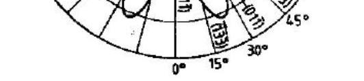
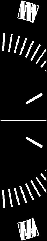
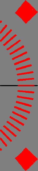
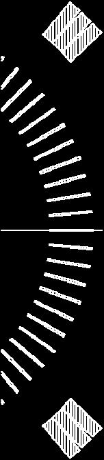
42 Wet Etch Test Pattern (1) Wagon wheel pattern mask Wagon wheel pattern - Size: 50 mm x 400 mm - Pattern repeated every 5 degree - Inner pattern : Pattern width 5 mm : Observation of slow etch rate -Outer pattern : Pattern width 300 mm Inner pattern : Observation of fast etch rate Outer pattern usage and possession is in violation of copyright laws 42


43 Wet Etch Test Pattern (2) Patterns defined by only photolithography Pattern Wet etch Oxide Silicon Wet etch result Patterns defined by deep Si etch Pattern Wet etch Wet etch result usage and possession is in violation of copyright laws 43
44 Wet etch rate inspection Wet Etch Test Pattern (3) W W etch Etch rate = W -W etch 2 usage and possession is in violation of copyright laws 44
45 (100) Si Wet Etch (1) {133} {133} K50m K70m K90m 40wt % KOH K50m: 50 K70m: 70 K90m: 90 usage and possession is in violation of copyright laws 45
 26.")
")


46 (100) Si Wet Etch (2) O {111} Minimum etch rate (110) Flat zone {133} Maximum etch rate usage and possession is in violation of copyright laws 46

 e.) H..Sede,J.")


47 (100) Si Wet Etch (3) EDP solution at 95 KOH solution at 78 Ref.) e.) H..Sede,J. Seidel, of Electrochemical e ca Society, 137(11), pp , usage and possession is in violation of copyright laws 47
 SEM")


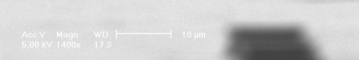
48 (100) Si Wet Etch (4) SEM view: (100) wafer, KOH 40%, 50 usage and possession is in violation of copyright laws 48
49 (100) Si Wet Etch (5) Micromachining of (100) wafer usage and possession is in violation of copyright laws 49
50 Anisotropic Silicon Etching (100) Si Wet Etch (6) Silicon nitride coating {111}planes (100)silicon wafer (c) (a) Heavily boron-doped region Openings patterned on nitride Hole (d) Diaphragm V-trench (b) (e) usage and possession is in violation of copyright laws 50
51 (100) Si Wet Etch (7) Nozzle Diaphragm usage and possession is in violation of copyright laws 51
52 (100) Si Wet Etch (8) Rectangular corner compensation for mesa structure fabrication Mask layout of compensation pattern for preventing undercut <110> <110> usage and possession is in violation of copyright laws 52
53 (100) Si Wet Etch (9) 45º rotated rectangular corner compensation for mesa structure fabrication <110> <100> <100> usage and possession is in violation of copyright laws 53
54 (100) Si Wet Etch (10) Application examples (1) Accelerometer Tube usage and possession is in violation of copyright laws 54
 (100) Si Wet")


55 Application examples (2) (100) Si Wet Etch (11) Holding structure over v-grooves Ink jet printer nozzle usage and possession is in violation of copyright laws 55
56 (110) Si Wet Etch (1) T50m T90m {771} 40wt % TMAH T50m: 50 T90m: {113} 150 usage and possession is in violation of copyright laws 56

")


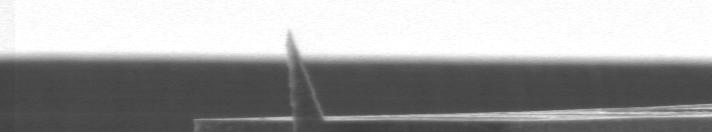
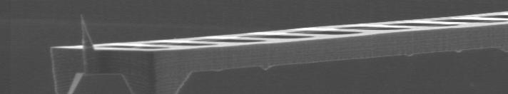
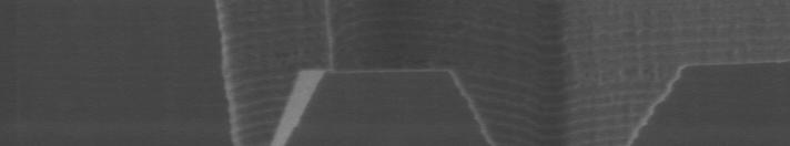
57 (110) Si Wet Etch (2) 84.2 o (771) Maximum etch rate (111) Minimum etch rate (113) 25.3 o 54.7 o (001) Flat zone usage and possession is in violation of copyright laws 57
 EDP")


58 (110) Si Wet Etch (3) EDP solution at 95 KOH solution at 78 Ref.) H. Seidel, J. of Electrochemical Society, 137(11), pp , 1990 usage and possession is in violation of copyright laws 58
 SEM")


59 (110) Si Wet Etch (4) SEM view: (110) wafer, KOH 40%, 50 usage and possession is in violation of copyright laws 59
60 (110) Si Wet Etch (5) Top and cross-sectional view of wet etched (110) silicon wafer -- B [111] 35.26º (100) - [111] A A - [111] -- [111] Mask [111] A-A cross-section -- - (111) (100) (111) B B-B cross-section usage and possession is in violation of copyright laws 60
 The planes")


 usage and")
61 Convex corners (110) Si Wet Etch (6) The planes that emerge under convex corners are not compatible with the planes that we find in the etch rate minima. Acute and obtuse convex corners of parallelogram Need compensation pattern for undercut and residues (SNU NML) usage and possession is in violation of copyright laws 61
62 (110) Si Wet Etch (7) Compensation pattern design using <111> beam <111> < 111> <111>direction compensation beams oblique to the wafer flat <111>direction compensation beams oblique to the wafer flat usage and possession is in violation of copyright laws 62
 Si")


63 Compensation results (110) Si Wet Etch (8) Good compensation effects on acute corners Need other compensation pattern on convex corners usage and possession is in violation of copyright laws 63
 Si")


64 Compensation results (110) Si Wet Etch (9) Good compensation effects on acute corners Need other compensation pattern on convex corners usage and possession is in violation of copyright laws 64
65 (110) Si Wet Etch (10) Rectangular compensation pattern design <110> direction <100> direction <110> direction i <100> direction usage and possession is in violation of copyright laws 65
66 Compensation results Large residues remain (110) Si Wet Etch (11) usage and possession is in violation of copyright laws 66
67 (110) Si Wet Etch (12) Triangular compensation pattern design <311> direction <771> direction <311> direction <771> direction usage and possession is in violation of copyright laws 67
 Compensation")


68 (110) Si Wet Etch (13) Compensation results - Very large unwanted residues at the bottom - Features sharp corners at the top of the structures Etch front place : 311 Etch front place : 771 usage and possession is in violation of copyright laws 68
69 (110) Si Wet Etch (14) Rhombic compensation pattern design - - <111> <111> -- <111> - <111> - - <771> - <113> -- <771> -- <113> usage and possession is in violation of copyright laws 69
 Si")


70 Compensation results (110) Si Wet Etch (15) Good compensation effects on both corners Very small unwanted residues at the bottom Features relatively sharp corners at the top usage and possession is in violation of copyright laws 70
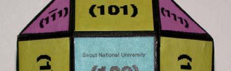
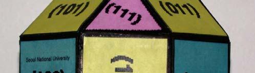
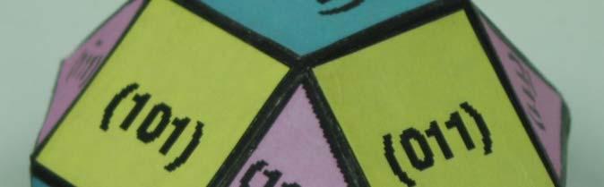
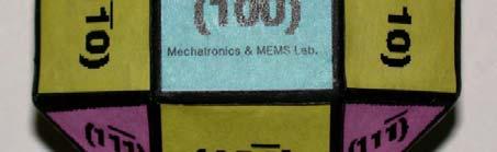
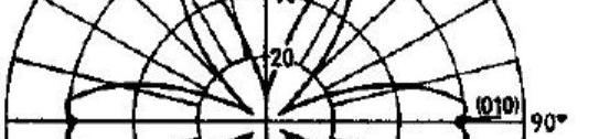
71 Crystallography of Si (111) (111) Si Wet Etch (1) [111] [111] [111] o A A' [111] [111] (111) [111] Cross section AA' o B 120 o 60 o B' [111] [111] 60 o Cross section BB' usage and possession is in violation of copyright laws 71
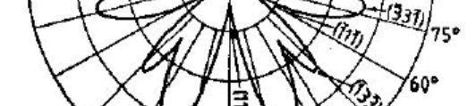
72 (111) Si Wet Etch (2) T50m T70m wt % KOH T50m: 50 T70m: {112} {431} {431} usage and possession is in violation of copyright laws 72


")


")

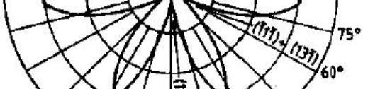
73 (111) Si Wet Etch (3) 46.1 o 13.9 o 30.0 o (314) Maximum etch rate (112) Minimum etch rate (134) Maximum etch rate (011) Flat zone usage and possession is in violation of copyright laws 73
 22 wt%")
 M.")


74 (111) Si Wet Etch (4) 22 wt% TMAH at 80 KOH at 80 Ref) M. Sekimura, MEMS99, 1999 Ref) B.C.S. Chou, C-N. Chen, and J-S. Shie, Sensors and Actuators A, vol. 75, 1999 usage and possession is in violation of copyright laws 74


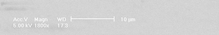
75 (111) Si Wet Etch (5) SEM view: (111) wafer, TMAH 10%, 50 usage and possession is in violation of copyright laws 75


76 (111) Si Wet Etch Application (1) 3 {111}-faceted tip Very sharp tip with 54.7 Convex compensation design 54.7 L 1 = 2 a sin R R usage and possession is in violation of copyright laws 76


77 (111) Si Wet Etch Application (2) 3 {111}-faceted tip (composed of (111),(111), (111) ) Wet etch time: 3 min Tip height: 5 µm 3 {111}-faceted tip usage and possession is in violation of copyright laws 77
78 (111) nano tip (111) Si Wet Etch Application (3) Consist of single (111) plane and two passivation planes Advantages Tip sharpness Ultra-sharp cone angle High-aspect ratio nano tip Stable wet etch properties Wet etch time Wet etch conditions (111) nano tip usage and possession is in violation of copyright laws 78


79 (111) Si Wet Etch Application (4) Single nano tip Tip height: 10 µm usage and possession is in violation of copyright laws 79


80 (111) Si Wet Etch Application (5) Specification of nano tip Cantilever Thickness: 8 µm Length: 250 µm Width: 30 µm Pitch: 200 µm Nano tip Height: 10 µm Aspect ratio: 31 3:1 Tip radius: 10 nm Total cone angle: 19.5 usage and possession is in violation of copyright laws 80
81 Limitation of Wet Etch Processing yield: dependent with etch stop method Time etch stop is simple but not reliable Electrochemical etch stop is reliable but complex Limited geometry freedom (crystal-direction dependence) Et Extensive real estate tt consumption &l large dimensioni Corner compensation However, for nozzles & grooves, proven mass production method (e.g. injector nozzles, ink jet printer nozzles, pressure sensors,...) usage and possession is in violation of copyright laws 81
82 Reference K. R. Williams, and R. S. Muller, Etch Rate for Micromachining Processing, Microelectromechanical Systems, Journal of, Vol. 5, No. 4, pp , 1996 K. R. Williams, K. Gupta, and M. Wasilik, Etch rates for micromachining processing-part II, Microelectromechanical Systems, Journal of, Vol. 12, No. 6, pp , 778, 2003 S. Lee, S. Park, and D. Cho, The Surface/Bulk Micromachining (SBM) process: anew method for fabricating released microelectromechanical systems in single crystal silicon, J. Microelectromechanical Syst., to appear Sept Kim, B. and Cho, D., Aqueous KOH Etching of (110) Silicon-Etch Characteristics and Compensation Methods for Convex Corners, J. of Electrochemical l Society, 145(7), pp , 2507 July 1998 H. Seidel, Anisotropic Etching of Crystalline Silicon in Alkaline Solution, J. of Electrochemical Society, 137(11), pp , Nov J.T.L. Thong, P. Luo, W.K. Choi, and S.C. Tan, Evolution of hillocks during silicon etching in TMAH, J. Micromech. Microeng. 11, pp , 2001 usage and possession is in violation of copyright laws 82
83 Reference C. H. Han and E. S. Kim, Fabrication of Dome-Shaped Diaphragm with Circular Clamped Boundary on Silicon Substrate, MEMS 99, pp , 1999 Kurt E. Petersen, Silicon as a Mechanical Material, Proceedings of The IEEE, 70(5), pp , May 1982 Melissa A. Hines, Understanding the Evolution of Silicon Surface Morphology during Aqueous Etching, Sensors and Materials, 13(5), pp , 2001 Paik S., Characteristics of (111)-oriented Silicon in Aqueous TMAH and its Applications, MS Thesis, Seoul National University, Marc J. Madou, Fundamentals of MICROFABICATION 2 nd edition, CRC Press, J. D. Lee, Silicon Integrated Circuit microfabrication technology 2 nd edition, Daeyoungsa, Gregory T. A. Kovacs, Micromachined Transducers Sourcebook 1 st edition, McGraw-Hill Science/Engineering/Math, S.M. Sze, Semiconductor sensors, JOHN WILEY & SONS, INC., 1994 usage and possession is in violation of copyright laws 83