STRUCTURAL AND ELECTRICAL PROPERTIES OF Sb 2 O 3 THIN FILMS
|
|
|
- Alisha Franklin
- 5 years ago
- Views:
Transcription
1 STRUCTURAL AND ELECTRICAL PROPERTIES OF Sb 2 O 3 THIN FILMS NICOLAE ÞIGÃU Faculty of Sciences, Dunãrea de Jos University of Galaþi, 47 Domneascã Street, , Romania ntigau@ugal.ro Received September 26, 2006 The thin films Sb 2 O 3 are deposited under vacuum on glass substrates by thermal evaporation technique. The structural characteristics of these films were studied by combined X-ray diffraction and planar view scanning electron microscopy. Electrical properties of vacuum evaporated Sb 2 O 3 thin films have been studied. The electrical conductivity was carried out at different temperatures in the range K. The electrical conduction was discussed in terms of known transport mechanisms. The thermal activation energy of the films with thickness of 0.34 μm is determined by the temperature dependence of electrical conductivity. Key words: Antimony trioxide, thin films, electrical conductivity, thermal activation energy. 1. INTRODUCTION Recently, the preparation of antimony trioxide (Sb 2 O 3 ) thin films has attracted much attention due to their potential application in optoelectronic and photoelectric devices [1 3]. The quality of these devices is strongly influenced by the deposition condition used for preparation of Sb 2 O 3 thin films. A study of correlation between the structural properties of thin films and their electrical conductivity is still necessary for more comprehensive understanding of this correlation and for the improvement of the quality of these films for the technological applications. Sb 2 O 3 thin films are generally prepared by various methods, such as thermal evaporation under vacuum, vapor condensation, hydrolysis and sol-gel method [1, 2, 4, 5]. In the present paper the structural and electrical properties of Sb 2 O 3 thin films evaporated in vacuum are investigated. The activation energy of electrical conduction in Sb 2 O 3 thin films was determined using the temperature dependence of electrical conductivity. Paper presented at the National Conference on Applied Physics, June 9 10, 2006, Galaþi, Romania Rom. Journ. Phys., Vol. 53, Nos. 1 2, P , Bucharest, 2008
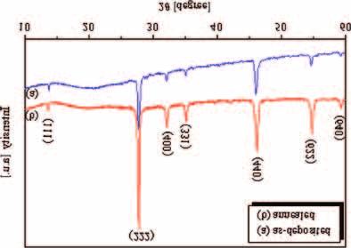
2 204 Nicolae Þigãu 2 2. EXPERIMENTAL Sb 2 O 3 thin films were deposited on glass substrates by thermal vacuum evaporation technique. The polycrystalline Sb 2 O 3 powder (99.99% purity) was sealed in ampoule at a pressure of torr and melted at 930 C. The sourcesubstrates distance of 80 mm was kept constant during the evaporation process. The glass substrates were maintained at room temperature (300 K) and rotated during film deposition to prevent non-uniformity in film thickness. The thickness of as-deposited films was calculated as d = 0.34 μm by using multiple beam interference technique [6]. After deposition of Sb 2 O 3 thin films, two vacuum aluminium electrodes at top surface were deposited for the electrical contact. The planar structure with the length l = 10 mm and electron separation b = 30 mm was used for electrical resistance measurements. A Keithley 6517A electrometer was used for resistance measurements in the temperature range of K. The electrical conductivity of Sb 2 O 3 thin films was determined according to relation σ = b/rdl, where R represents the measured electrical resistance of films. X-ray diffraction (XRD) characterization of Sb 2 O 3 thin films was carried out using filtered CuK α radiation (λ = Å) with a Dron 3 diffractometer. The X-ray tub was operated at voltage of 32 kv and current of 20 ma. The morphology of the film surface was investigated by scanning electron microscopy (SEM) technique using a scanning electron microscope, type Philips SEM 515, operated at 12.6 kv. 3. RESULTS AND DISCUSSION For Sb 2 O 3 thin films deposited onto unheated substrates was experimentally established that the samples with stable structure and reproducible physical properties can be obtain if, after deposition, they are subjected to some heat treatments [7]. These treatments consist of two successive heating and cooling cycles within a certain temperature range K. Fig. 1 shows the X-ray diffractograms of Sb 2 O 3 thin films, with the thickness of 0.34 μm, before (curve a) and after repeated heating-cooling cycles (curve b). The structural analysis, performed by XRD, indicate that the studied Sb 2 O 3 thin films, are polycrystalline in nature and have a cubic structure. The indexing of peaks of this structure is reported in Fig. 1. The lattice parameter of cubic structure was found to be a = Å, which is consistent with the standard value (JCPDS , a = Å). Sb 2 O 3 thin films were found to exhibit seven diffraction peaks associated with (111), (222), (400), (420), (440), (622) and (640) reflection planes, of which the intensity of the (222) orientation is very predominant. The heat treatment not
 peak and decrease in the full-width at half-maximum (FWHM), which indicates an improvement in the")
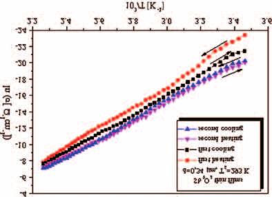
3 3 Structural and electrical properties of Sb 2 O 3 thin films 205 changes the XRD pattern and the structure remains as that of as-deposition films. However, the X-ray pattern of the annealed film shows a strongly increase in intensity of (222) peak and decrease in the full-width at half-maximum (FWHM), which indicates an improvement in the crystallinity of the film and increase in the grain size of crystallites after thermal annealing. This increase in grain size is clearly revealed from SEM analysis. Fig. 2(a) and (b) shows the SEM micrographs of surface morphologies of the Sb 2 O 3 thin films before and after thermal treatment, respectively. From both the micrographs it shows that the films are dense, smooth and have a compact structure. Fig. 2 SEM micrographs of Sb 2 O 3 thin films: (a) as-deposited, (b) annealed. It is shown that the morphology of the Sb 2 O 3 thin films is strongly affected by thermal treatment. The SEM micrograph of annealed film clearly shows the improvement in crystallite size of Sb 2 O 3. After thermal treatment, grain size of Sb 2 O 3 thin films becomes larger and the morphology becomes denser. The creation of larger grains is as a result of coalescence of small grains into bigger one, which can be seen from Fig. 2(b) [8, 9]. As a result the number of grain boundaries decrease. Fig. 3(a) and (b) shows lognormal distribution curves [10] for mean diameter of crystallites corresponding of Sb 2 O 3 thin films before and after thermal annealing, respectively. The crystallites of as-deposited Sb 2 O 3 thin films have the mean diameter in the range 4 20 nm, with an average diameter of 7.11 nm, while the mean diameters of annealed film are in the range nm, with an average diameter of nm. The temperature dependence of dark electrical conductivity of Sb 2 O 3 thin films was studied by using dc two-probe method to determine the thermal activation energy. These studies are carried out in the temperature range K. The typical dependences obtained for Sb 2 O 3 thin films are presented in Fig. 4. The experiments showed that after two successive heating and cooling cycles in the same temperature range, the dependence of the electrical conductivity
4 206 Nicolae Þigãu 4 Fig. 3 Mean diameter distribution for Sb 2 O 3 thin films (a) as-deposited, (b) annealed. becomes reversible. This fact indicates the stabilization of the film microstructure in the investigated temperature range [11]. From Fig. 4 it can be seen that the electrical conductivity of Sb 2 O 3 thin films increases with increasing temperature, showing semiconductor-like behavior in the whole temperature range investigated. The electrical conductivity at room temperature, before heat treatment, σ r, was found to be about Ω 1 cm 1. After first heating the electrical conductivity at temperature 443 K the electrical conductivity of Sb 2 O 3 thin films increase at value σ m = = Ω 1 cm 1. Finally, after two successive heating and cooling cycles, the electrical conductivity of Sb 2 O 3 thin films becomes σ f = Ω 1 cm 1. It may be assumed that the increase in electrical conductivity of the annealed Sb 2 O 3 thin films was due to improvement in crystallite and grain size, decrease in density of grain boundary intercrystallite and removal of some impurities [11 14]. Also, from Fig. 4 it can be observed a linear dependence of lnσ versus 10 3 /T for each heating or cooling process. This suggest that the electrical conductivity of Sb 2 O 3 thin films, σ, varies with the temperature according to the Arrhenius relation [15 17]: Δ ( ) σ=σ0 exp E (1) kt
5 5 Structural and electrical properties of Sb 2 O 3 thin films 207 where σ 0 is a parameter depending on the semiconductor nature, k is the Boltzmann constant and ΔE is the thermal activation energy. From the slope of lnσ versus 10 3 /T dependences, the values of ΔE were calculated for each heating and cooling process. It was found that the activation energy of electrical conductivity decrease from 1.01 ev, corresponding of first heating process, to 0.94 ev after two successive heating and cooling cycles. The obtained values of activation energy strongly differ from the values of band gap energy, E g = ev, determined by optical measurements for Sb 2 O 3 thin films [1, 18, 19]. This suggests that the determined values of activation energy correspond to shallow donor or deep acceptor level located in the forbidden band of Sb 2 O 3 [14]. 4. CONCLUSIONS Sb 2 O 3 thin films with thickness of 0.34 μm were deposited onto unheated glass substrates by thermal evaporation under vacuum (p = torr). After deposition Sb 2 O 3 thin films were subjected at two successive heating and cooling cycles. It was found that the heat treatment results in stabilization of Sb 2 O 3 thin films structure and the temperature dependence of the electrical conductivity become reversible. Crystal structure performed by XRD revealed that the asdeposition Sb 2 O 3 thin films were polycrystalline in nature with cubic structure and the crystalline structure improves after heat treatment. From SEM analysis the mean grain size distribution was determined. It was found that the average diameter of crystallites increase from 7.11 nm to nm after annealing treatment. Also, the experimental results showed that the dark electrical conductivity of Sb 2 O 3 thin films increase from Ω 1 cm 1 to Ω 1 cm 1 after first heating process presented a semiconductor-like behavior. The value of the activation energy estimated from temperature dependence of electrical conductivity ranged between 0.94 ev to 1.01 ev. The changes in the electrical conductivity and activation energy are determined to improvement of polycrystalline structure and increase in grain size after thermal treatment. REFERENCES 1. N. K. Sahoo, K. V. S. R. Apparao, Process-parameter optimization of Sb 2 O 3 films in the ultraviolet and visible region for interferrometric application, Appl. Phys. A, 63, (1996). 2. Y. Zhang, G. Li, J. Zhang, L. Zhang, Shape-controlled growth of one-dimensional Sb 2 O 3 nanomaterials, Nanotechnology, 15, (2004). 3. Q. Keqiang, Z. Rongliang, Research on preparation of nanometer antimony trioxide from slag containing antimony by vacuum evaporation method, Vacuum, 80, (2006).
6 208 Nicolae Þigãu 6 4. D. Zeng, C. Xie, B. Zhu, Characteristics of Sb 2 O 3 nanoparticles synthesized from antimony by vapor condensation method, Mater. Lett., 58, (2004). 5. Y. Lisong, W. Renyong, Z. Qifa, Preparation and retarding characteristics of nanometer Sb 2 O 3 retarding ultrafine powder, Mater. Eng., 12, 9 12 (1999). 6. S. Tolansky, Multiple-beam interference. Microscopy of metals, Academic Press, New York, N. Þigãu, V. Ciupina, G. Prodan, G. I. Rusu, C. Gheorghies, E. Vasile, The influence of heat treatment on the electrical conductivity of antimony trioxide thin films, J. Optoelectron. Adv. Mater. 5, (2003). 8. R. B. Kale, C. D. Lokhande, Room temperature deposition of ZnSe thin films by successive ionic layer absorption and reaction (SILAR) method, Mat. Res. Bull., 39, (2004). 9. N. A. Shah, A. Ali, A. K. S. Aquili, A. Maqsood, Physical properties of Ag-doped cadmium tellurid thin films fabricated by close-space sublimation technique, J. Cryst. Growth, 290, (2006). 10. V. Kapaklis, P. Poulopoulos, V. Karoutsos, Th. Monouras, C. Politis, Growth of thin Ag films produced by radio frequency magnetron sputtering, Thin Solid Films, 510, (2006). 11. G. I. Rusu, M. E. Popa, G. G. Rusu, I. Salaoru, On the electronic transport properties of polycrystalline ZnSe films, Appl. Surf. Sci., 218, (2003). 12. P. Arun, P. Tyagi, A. G. Vedeshwar, V. K. Paliwal, Ageing effect of Sb 2 Te 3 thin films, Pysica B, 307, (2001). 13. P. Arun, A. G. Vedeshwar, Influence of grain size on the electrical properties of of Sb 2 Te 3 polycrystalline films, Mat. Res. Bull., 38, (2003). 14. R. B. Kale, C. D. Lokhande, Influence of air annealing on the structural, morphological, optical and electrical properties of chemically deposition ZnSe thin films, Appl. Surf. Sci., 252, (2005). 15. A. F. Qasrawi, N. M. Gasanly, Temperature effect on dark electrical conductivity, Hall coefficient, space charge limited current and photoconductivity of TlGaS 2 single crystal, Semicond. Sci. Technol., 20, (2005). 16. F. Yakuphanoglu, M. Sekerci, E. Evin, The determination of the conduction mechanism and optical band gap of fluorescein sodium salt, Physica B, 382, (2006). 17. A. S. Maan, D. R. Goyal, S. K. Sharma, T. P. Sharma, Investigation of electrical conductivity and optical absorption in amorphous In x Se 100 x alloys, J. Phys. III France, 4, (1994). 18. N. Þigãu, V. Ciupina, G. Prodan, The effect of substrate temperature on the optical properties of polycrystalline Sb 2 O 3 thin films, J. Cryst. Growth, 277, (2005). 19. N. Þigãu, Preparation and characterization of Sb 2 O 3 thin films, Rom. J. Phys. 51, (2006).
7
8