Fraunhofer IZM Bump Bonding and Electronic Packaging
|
|
|
- Peregrine Pope
- 5 years ago
- Views:
Transcription

")

1 Fraunhofer IZM Bump Bonding and Electronic Packaging Fraunhofer Institute for Reliability and Microintegration (IZM) Gustav-Meyer-Allee Berlin Germany Dipl.-Ing. Thomas Fritzsch Contact: 1


2 Agenda Tooling and processes at Fraunhofer IZM Bump bonding: Bump size and pitch, wafer and chip size, alternative bonding, thin chip bonding Future Developments: RDL, Interposer, Thin Wafer Handling, 3D - TSV Chip to Wafer -, Wafer to Wafer - Assembly 2


3 Overview Fraunhofer Gesellschaft 60 institutes 20,000 employees app. 1.8 billion turnover app. 70% contract research Information Technology Light & Surfaces Life Sciences Micro Electronics Production Defense & Security Materials & Components 3


4 Fraunhofer IZM Facts founded 1993 Figures Mio. turnover 77 % contract research More than 350 employees (app. 200 full time, 150 PhD, trainee) Berlin Locations Dresden Oberpfaffenhofen Director Prof. Dr. Klaus-Dieter Lang Core Competencies Wafer Level System Integration Substrate Level System Integration Materials & Reliability System Design Material characterisation Process evaluation Reliability testing Failure analysis Sample production Training courses 4


5 Fraunhofer IZM Dresden Fraunhofer IZM-ASSID Berlin Fraunhofer IZM Oberpfaffenhofen Fraunhofer IZM-ZVE 5


6 Wafer Level Integration Technologies Fraunhofer IZM - Berlin Fraunhofer IZM - ASSID ~ 800 m² cleanroom Wafer size: 100, 150, 200, (300)mm 900 m² cleanroom Wafer size: 200, 300mm PVD Sputtering DRIE Si Etch CVD (Oxid / Barrier / Seed) Lithography Electrochemical deposition and Wet Etch Thinning CMP Temporary Bonding and Debonding Die & Wafer Bonding D2W, D2D, D2S, W2W Singulation Solder Ball Attach Automatic Optical Wafer Inspection Metrology 6


7 Wafer Level Packaging (WLP) Wafer Level Packaging on 100, 150, 200 and 300mm wafer Fine Pitch Bumping Chip Scale Packaging Thin Film Multilayer Substrates 3D Integrated Systems 7


 Resist patterning by mask")
 Solder material deposition (SnPb, SnAg,")
8 Wafer Level Packaging for Hybrid Pixel Detectors Solder Bump Deposition SnAg3.5 Indium Cu-Sn Pillar Au-Sn Formation of Interconnect on Readout Chip side: Sputtering of adhesion layer / diffusion barrier (Ti:W, Ti, Cr, ) Sputtering of plating base (Cu, Au, Ni, ) Resist patterning by mask lithography UBM deposition (electroplating, evaporation, ) Solder material deposition (SnPb, SnAg, In, AuSn, CuSn, ) Reflow (optional) Wafer Dicing 8


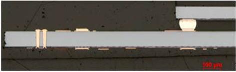
9 Wafer Level Packaging for Hybrid Pixel Detectors Deposition of solderable pixel pads on sensor wafer Bump metal SnPb37 SnAg3.5 Au80Sn20 Pad metallization Cu-Ni-Au Cu, Ni-Cu, Ni-Au Au Au Ni Cu FIB cross section of electroplated Cu-Ni-Au pixel pad 9


10 PVD Sputtering of Plating Base Metal deposition: TiW, Ti, Cu, Au, Pt, NiCr, Al, AlSi, Layer thickness: nm Goals: minimum layer stress Diffusion barrier between contact pad and plating base Plating base layer with low resistivity 10


11 Resist Patterning by Mask Lithography Resist deposition by spin-coating, spray-coating or dry film lamination Resist thickness 2µm 100µm UV mask exposure Resist development Goals: Accurate wafer-mask alignment Edge steepness/resist stability Residue free via 11

12 Electrochemical Deposition - Electroplating Metal deposition: Cu, Au, Ni, Sn, SnAg, In, Au/Ag Layer thickness: 2 100µm Goals: Minimum layer stress Homogenious layer thickness G Rack Plater C A: Anode B: Spray Tubes A B D E C: Shielding D: Wafer E: Overflow F: Immersion Heater F G: Level Switch 12


13 High Accuracy Flip Chip Assembly Karl Suss / SET FC150 Panasonic FCB3 Accuracy: ± 1 µm at 3 cycle time: ~1-2 min. per die maximum die size: 2 x 2 maximum substrate size: 6 x 6 heating profiles from top and bottom minimum alignment mark size: 20 µm accuracy: 3 µm at 3 full automatic FC bonder with feeder unit pick & place cycle time: <2 s maximum substrate size: 300 mm wafer TC and TS bonding head 13
14 High Accuracy Flip Chip Assembly CuSn-Pillar AuSn Nanoporous interconnects SnAg CuSn Cu-Cu Au ep Cu-Sn (TLPB) Flip Chip Sn, SnAg(Cu), CuSn Au/Sn fluxless Gold Indium Reflow soldering Cu-Sn Transient Liquid Phase Bonding (TLPB) Thermode Bonding / Metal- Metal Direct Bonding Thermo-compression Thermosonic Substrates: Chip to Chip Chip To Wafer Wafer to Wafer 14


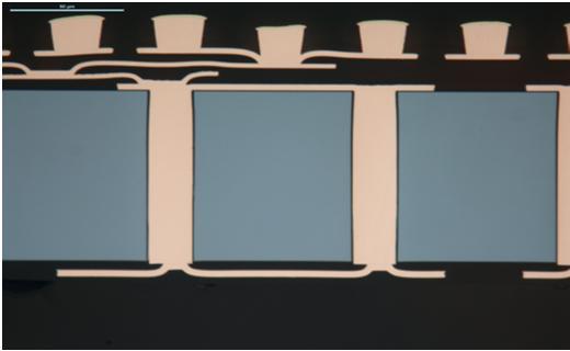
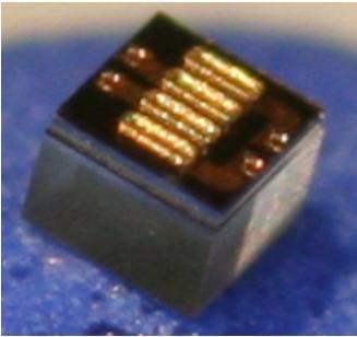
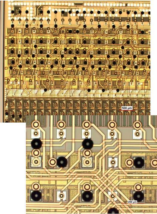
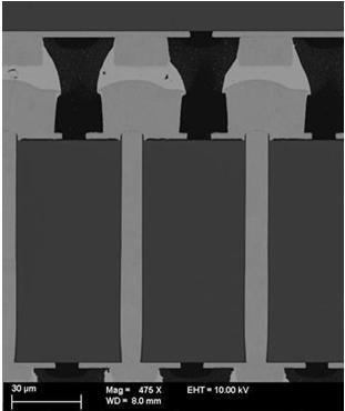
15 Fine Pitch Bumping and Metallization state of the art Bumping: Pitch 20 50µm ca SnPb Diameter: 10 µm Pitch: 20 µm from SnAg Diameter: 25 µm Pitch: 55 µm (matrix) Fineline Structures: 4µm line width / 4µm space 2 7µm height Example: Double Layer Microcoil Low volume production for industrial customer on 200mm wafer Smaller bump pitch below 50µm possible but not requested so far 15
, 450µm (y2) Chip Size: ~20 x 20 cm² Bump matrix: 80 x 336 (26880 per chip) Number of")
 Application: Research Bump size: 25 30µm Bump Pitch: 55µm (x, y) Chip Size: ~14 x 16 cm² Bump")
16 Chip Size and Bump Density state of the art on 200mm ATLAS FE-I4 MEDIPIX2 / MEDIPIX3 Bump size: 25µm Bump Pitch: 50µm (x, y1), 450µm (y2) Chip Size: ~20 x 20 cm² Bump matrix: 80 x 336 (26880 per chip) Number of bumps: >1.6 Mio. (200mm) Application: Research Bump size: 25 30µm Bump Pitch: 55µm (x, y) Chip Size: ~14 x 16 cm² Bump matrix: 256x257 (65792 per chip) Number of bumps: >7 Mio. (200mm) Application: Research, Industry 16

: > 0,014 Stress")


17 Wafer Thinning Technology Thinning process: Mechanical Si grinding: grit size, Ra (µm): > 0,014 Stress relief: Dry Polishing Ra (µm): 0,009 0,0003 CMP (Chemical Mechanical Polishing) Wet chemical etching Plasma etching (source DISCO) Dry Polishing CMP Wet Etching Dry Etching (source DISCO) 17


18 Thin Wafer Handling Temporary Wafer Bonding Thin Wafer Handling Systems Solvent Release of perforated Carriers Laser Release of Glass Carriers Slide-Off Release Tilt-Off Release Dissolution of glue by solvent enabled by holes in carrier wafer Destruction of glue layer by laser radiation Separation of Wafers by shear force at elevated temperatures Separation of Wafers by glue dissolution in rim area and following tilt-off release TSV-Wafer TSV-Wafer Support Wafer Support Wafer (source SUESS MicroTec Photonic Fraunhofer IZM Systems Inc. ) thomas.fritzsch@izm.fraunhofer.de 18


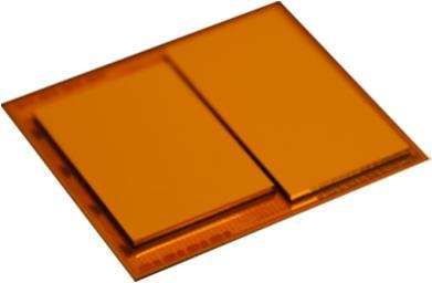
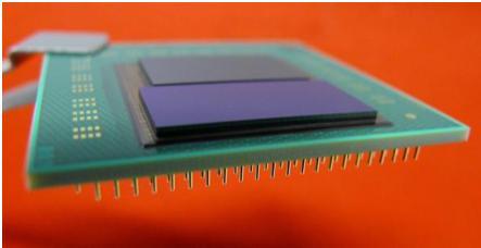
19 Thin Chip Assembly using Transparent Carrier FE-I4 ROC ATLAS IBL production: Size ~2x2cm², thickness 150µm More than 600 modules processed (single 3D, planar double) TIMEPIX single chip hybrids: Size ~14x16cm², TIMEPIX thickness 100µm 6 sensor, thickness 100µm ALICE ROC size test chips, 5-Chip module: ROC Size: 14x16mm², thickness 50µm 4 Sensor, 100µm thickness 19
20 Future Developments Integration Technology from 2D to 3D 3D Stacking Alterantive Bonding Techniques Wafer Sizes 20


21 Integration Technology 2D SiP Redistribution 2.5D SiP TSV Silicon Interposer 3D IC TSV in active IC 21


22 3D Stacking Chip 2 Chip Chip 2 Wafer Wafer 2 Wafer Flip Chip Bonder Tools: High Accuracy Chip Pick and Place Chip or wafer substrate Interconnection by temperature and pressure Wafer Bonder Tools: Wafer to wafer alignment bonding by temperature and pressure 22
 Bonding")


 Bonding")
23 Bonding Techniques for 3D Integration Solder bump bonding Transient Liquid Phase (TLP) Bonding Metal-Metal Direct Bonding Cu CuSn Cu Cu Cu 3 Sn Intermetallics ECD Cu-pillar with solder cap Short reflow process Self-alignment ECD Cu and Cu-Sn pads High melting Cu 3 Sn IMC Bonding parameters: T, F, t High planarity necessary ECD Cu pads Planarized surfaces Bonding parameters: T, F, t (vacuum) Bonding temperature 300 C 400 C 23
 Thickness: SEMI standard 750µm, thinned to 250")

24 Wafer Size Sensor Wafer Currently 4 and 6 Thickness µm Future: 8 and 100µm? Readout Wafer Size: 8 (i.e.130nm IBM) Thickness: SEMI standard 750µm, thinned to µm Future: 300mm and thinned to? Question: Double side processing Wafer handling Question: test source, bumping source Thin wafer handling and thin chip flip chip bonding 24


25 Thank You For Your Attention 25