MEMS Devices. Fraunhofer Institute for Silicon Technology ISIT. Itzehoe, Germa. any
|
|
|
- Violet Neal
- 5 years ago
- Views:
Transcription
1 Examples of CMP Processess for the Manufacturing of MEMS Devices Gerfried Zwicke er Fraunhofer Institute for Silicon Technology ISIT Itzehoe, Germa any
2 Contents MEMS Products and Market Comparison CMP for MEMS vs. Microelectronics poly-si angular rate sensor infrared digital micro mirror array capacitive RF-MEMS switch Future developments Opportunities for CMP consumables manufacturers Summary Page 2


3 Pioneering Work by Sandia (1995) Examples from Sandia s MEMS gallery comb drive 3 layer poly-si indexing motor bugs on devices spider mite on mirror assembly Courtesy Sandia National Laboratories. More pictures and movies (!) : Page 3
4 MEMS applications and products Automotive Aeronautics Consumer Micro-Electro Mechanical Systems (MEMS) products and markets pressure & air flow sensors, accelerometers, gyroscopes pressure sensors, gyroscopes ink jet heads, inertial MEMS, DLPs, Si microphones Defense inertial MEMS (for munitions guidance) Industrial Medical & Life Sciences Telecom pressure sensors, liquid flow sensors microfluidics for drug delivery or diagnostics RF-MEMS, micro relays (Source: Yole Développement market research) Page 4
5 Micro-Electro Mechanical Systems (MEMS) products and markets MEMS market outlook Year Market Units E&M Market (chip level) (Chemicals) 2006 US$ 6.5 B 1,700 0M 2007 US$ 7.0 B 2,1000 M 125 M 2008 US$ 7.8 B 2,6000 M 2009 US$ 8.7 B 3,200 0M 2010 US$ 9.7 B 4,3000 M 2011 US$ 11.3 B 5,8000 M 2012 US$ 13.9 B 6,7000 M > US$ 1 B 228 M (Source: Yole Développement market research) Page 5
6 Microelectronic vs. MEMS comparison of requirements affecting CMP MEMS specifics: Larger structures 1 µm 1 mm Thicker layers µm Relaxed planarity requirements exception: opto-mems Additional materials metals, polymers, ceramics Smaller substrates mm, change to 200 mm Other substrate s than Si glass, ceramic, metal, polymer Reduced cleanliness requirements exception: wafer bonding Reduced defect requirements roughness, scratches Production smaller unit numbers Page 6
7 CMP in MEMS Production who is already using CMP? Only a few mass products are manufactured using CMP: Accelerometers, gyros DLPs, micromirror arrays Hard disk drives R/W heads... poly-si CMP oxide planarizat tion Ni, Fe, Cr polishing e.g. Bosch e.g. Texas Instruments e.g. Seagate CMP is not yet anchored in the heads of MEMS development engineers Versatility of CMP processes has to be demonstrated and published Page 7
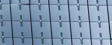
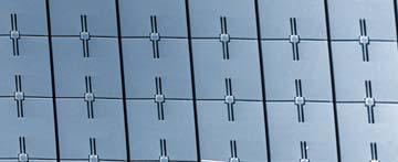
8 case studies poly-si angular rate sensor infrared digital micro mirror array capacitive RF-MEMS switch Page 8

")

,")

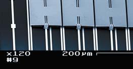
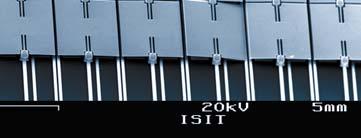
9 poly-si angular rate sensor Goal Moving poly-si comb (capacitor) structures for acceleration and angular rate sensors (gyros), height >10 µm, space 1 µm. Coriolis-force angular rate sensor Page 9


10 poly-si angular rate sensor Problem Thick poly-si (> 10 µm) layers show a rough surface after deposition (R a 1 µm) CMP Page 10
11 CMP poly-si angular rate sensor Sensor fabrication sequence: poly-si - Deposition of sacrificial oxide - Etching of anchor openings sacrificial oxide substr rate - Deposition of thick poly-si (>10 µm) - CMP of poly-si - Etching of comb structures by DRIE poly-si substrate - Etching of sacrificial oxide by vapour phase HF etch Page 11
12 poly-si angular rate sensor CMP results Poly-Si CMP Starting poly-si thickness 14 µm Final poly-si thickness = 11,35 µm Final poly-si lay yer non-uniformity < ± 200 nm (range) CMP Process Cabot SS25 fum med silica based SiO 2 slurry Removal Rate 0.5 µm/min WIWNU < 2% (~ ~55 nm (1 σ)) on 150 mm wafers R a nm after Fujimi Glanzox buff Page 12


13 poly-si angular rate sensor Sensor + ASIC in MCM: Signal range ± 300 /s Signal bandwidth Hz Applications: Vehicle dynamic control Car navigation Virtual reality Development Partner: SensorDynamics AG Page 13
14 case studies poly-si angular rate sensor infrared digital micro mirror array capacitive RF-MEMS switch Page 14


15 infrared digital micromirror array 256 x 256 pixel micro-mirror array for infrared imaging system Page 15
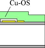
16 infrared digital micromirror array CMP 3: Cu sacrificial layer 10 µm thickness stop on Ni posts CMP 2: Cu damascene incl. TaN barrier CMP 1: Oxide planarization of CMOS passivation 2,5 µm SiO 2 0,7 µm SiON Wafer w/ CMOS circuit 3 CMP steps needed in the fabrication process Page 16
17 infrared digital micromirror array Results of thick Cu CMP 3 Cu-CMP slurry: Commercial product with inherently high selectivity to Nickel (Cabot icue 5003) on IC1000 k-grv. Removal rate > 0.5 µm/min Polishing time > 5 min, in-situ it conditioning i Roughness R a < 3 nm High selectivity to Nickel posts achieved Dishing between Nickel posts < 100 nm for mirrors 80 x 80 µm size sufficiently flat for IR applications Page 17


18 infrared digital micromirror array Final device Mirror array with tilted mirror after CMP 3 and copper sacrificial layer etch Page 18
19 case studies poly-si angular rate sensor infrared digital micro mirror array capacitive RF-MEMS switch Page 19


20 capacitive RF-MEMmanufactured with Cu sacrificial switch layer anchoring membrane actuation electrodes signal line dielectric layer schematic 3D-view of capacitive switch 20 GHz capacitive RF-MEMS switch Page 20
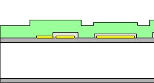
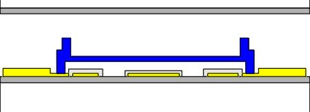
21 capacitive RF-MEMS switch Manufacturing flow of RF-MEMS: CMP Page 21
22 capacitive RF-MEMS switch Final Cu sacrif.-layer thickness: 2.85 µm 1200 Which Cu starting thickness is required for a planarity < 50 nm? 1 µm pattern height reduction depending on polishing time (removal) P consumables set (pad, slurry) Cu start thickness: 4.5 µm 1.65 µm Cu to be removed by CMP Pattern Height [nm m] ,2 0,4 0,6 0,8 1 1,2 1,4 1,6 Removal [µm] Cu-Slurry 1 / Pad A Cu-Slurry 2 / Pad B Page 22

 unpolished")


23 capacitive RF-MEMS switch Evolution of planarity (Cu-Slurry 2 / Pad B) unpolished pattern height 1000 nm micromap 512 white-light interferometer 0.64 µm mean removal pattern height 346 nm 1.51 µm mean removal pattern height 17 nm R a (plane) = 2.0 nm Page 23


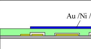
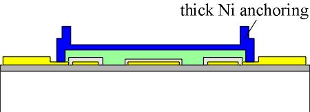
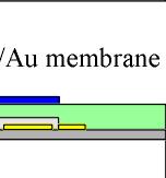
24 capacitive RF-MEMS switch v 2.0 Simultaneous formation of Cu sacrificial layer and membrane contacts Conventional RF-switch: Au lines, Ni anchoring & contact RF-switch with damascene contacts: Au lines, Cu contacts, SiO 2 anchoring Page 24


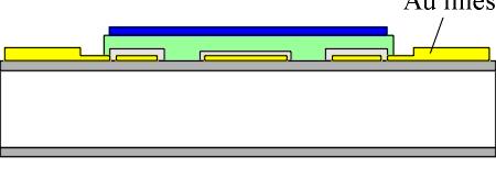
25 Cu damascene contacts: SiO Cu 2 capacitive RF-MEMS switch v 2.0 sacrificial layer contact after Au/Ni/Au membrane deposition and sac. layer etch SiO 2 Cu before CMP 3.6 µm oxide 5 µm copper after Cu/oxide CMP 3.2 µm oxide copper contacts and sac. layer SiO 2 Cu contacts SiO 2 anchoring Page 25
26 capacitive RF-MEMS switch Encountered Problems: Layer stress: 5 µm Cu leads to a wafer deformation of 150 µm Planarization of 3.6 µm high steps slurry Overpolish into SiO 2 to achieve oxide planarity slurry with 1 : 1 selectivity required Low dishing for flat membrane to avoid buckling with high Cu RR of > 500 nm required Various pad/slurry combinations and/or process schemes under evaluation Page 26
27 Further Examples applications of CMP for MEMS-related fabrication Wafer bonding Si-CMP for direct wafer bonding oxide CMP for anodic bonding grinding/polishing of glass frit for laser soldering (encapsulation of micro sensors) Backside CMP grinding/polishing of Si - replacement of double-side polished wafers - ultra-thin silicon: stress relief after grinding 3D integration (TSVs) metal CMP for removal of material overburden Page 27
28 Opportunities for the CMP Consumables Manufacturers Polishing pads larger structures require stiffer pads w/ low defectivity other pad/sub-pad combinations to be tested Polishing slurries thicker layers need higher RRs: customized solutions new/other ma aterials to be CMPed Conditioners adapted conditioners for more aggessive polishing Brush rollers 3D structures: danger of brush tear out Cleaning chemicals layer-specificc solutions needed Page 28
29 Outlook MEMS market volume nearly doubles from , number of units triples Expansion on new applications and additional layer materials: CMP? SiC, Si 3 N 4, SiGe, Ge (sac. layer, H 2 O 2 etch), Ni, Au amorphous/polycrystalline CVD diamond (high wear resistance, hydrophobic, chemically innert) low-cost substrates: glass, polymers, metals, ceramic piezo materials (PZT) for actuators... Page 29
30 Summary CMP is an enabling technology for the manufacturing of advanced inte egrated circuits CMP is deployed increasingly for the fabrication of modern MEMS devices CMP technology requirements: - ever decreasing device structure dimensions in microelectronic manufacturing - large structure dimensions in MEMS fabrication Future trends : 3D integration, ti packaging, new materials, new applications Page 30
31 Thank You Page 31