Electronic Supplementary Information
|
|
|
- Bennett Bradford
- 5 years ago
- Views:
Transcription
1 Electronic Supplementary Material (ESI) for Nanoscale. This journal is The Royal Society of Chemistry 2016 Electronic Supplementary Information Co-sputter Deposited Nickel-Copper Bimetallic Nanoalloy Embedded Carbon Films for Electrocatalytic Biomarker Detection Shunsuke Shiba, a,b,c Dai Kato, b Tomoyuki Kamata b,d and Osamu Niwa a,b a. Advanced Science Research Laboratory, Saitama Institute of Technology, Fusaiji, 1690, Fukaya, Saitama , Japan. b. National Institute of Advanced Industrial Science and Technology, 1-1-1, Higashi, Tsukuba, Ibaraki , Japan. c. Graduate School of Pure and Applied Sciences, University of Tsukuba, Tennodai, Tsukuba, Ibaraki , Japan. d. Chiba Institute of Technology, , Tsudanuma, Narashino, Chiba , Japan niwa@sit.ac.jp Contents Page Figure S1. The concept of UBM co-sputtering for fabricating nanoalloy embedded carbon film...s2 Figure S2. HRTEM image of the (a) NiNP embedded carbon film and (b) Ni 32 Cu 68 nanoalloy embedded carbon film S3 Figure S3. High-resolution C1s spectra for Ni 61 Cu 39 nanoalloy embedded carbon film....s4 Figure S4. Conditions for the each TEM observations shown at Fig. 1(b) and Fig. 2(c) S4 Figure S5. Repeated CVs of (a) Ni 64 Cu 36 nanoalloy embedded carbon film and (b) Ni 70 Cu 30 alloy film S5 Figure S6. Amperometric detection of D-mannitol obtained with Ni 64 Cu 36 nanoalloy embedded carbon film in the presence of chloride ions S5 Table S1. Sputter conditions for each layer in the stepwise deposited film and the properties of nanoalloys.. S6 Table S2. Sputter conditions and XPS results for the resultant films......s6 Table S3. Conditions of continuous flow measurements using radial flow cell.... S7 S1


2 Fig. S1 The concept of UBM co-sputtering for fabricating nanoalloy embedded carbon film. This consists of carbon, Cu and Ni targets focused on the center of the substrate surface. This configuration and individually controlled system allows us to form the homogeneous films with a large area while controlling the compositions of the bimetallic nanoalloys in the film over a wide range. The UBM system also enables us to irradiate Ar ions during deposition, and its energy is controllable by changing the substrate bias voltage. This allows us to change the structure of the carbon film including the surface smoothness, its sp 2 /sp 3 ratio, and possibly the ordering and size of the nanoalloys. Our method can fabricate an NP embedded structure by freely controlling the above parameters such as nanoalloy size, composition and surface roughness. This controllability is difficult to realize by similar co-sputtering system reported recently, where two targets of Ni-Cr alloy and silver were used to form the Ni-Cr nanoalloy embedded in Ag matrix (Bohra, M. et al., Sci. Rep., 6, 2016, ). S2

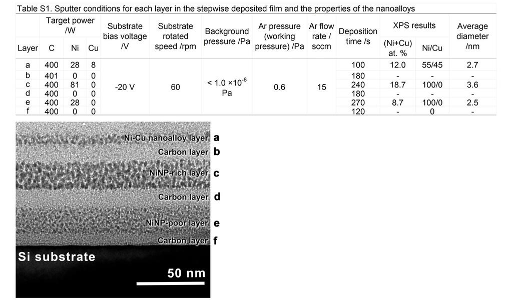
3 Fig. S2 HRTEM images of the (a) NiNP embedded carbon film and (b) Ni 32 Cu 68 nanoalloy embedded carbon film. Atomic metal percentages and average diameter s of these films are summarized in Table 1. S3
 spectrometer was used and the analysis was according to a previous report. 18 Each chemical bond ratio (sp 2 /sp 3 ) was estimated using Shirley s method attributed to 284.")
, FEI")

4 Binding energy / ev Fig. S3 High-resolution C 1s XPS spectra for Ni 61 Cu 39 nanoalloy embedded carbon film. A Shimadzu/Kratos model AXIS Ultra (AlKα ev) spectrometer was used and the analysis was according to a previous report. 18 Each chemical bond ratio (sp 2 /sp 3 ) was estimated using Shirley s method attributed to ev for sp 2 bonds (blue) and ev for sp 3 bonds (red). Fig. S4 The cross-sectional structure and elemental composition of the Ni 61 Cu 39 nanoalloy embedded carbon film were investigated with an analytical transmission electron microscope (TEM), FEI Tecnai Osiris operated at 200 kv, equipped with an energy-dispersive X-ray spectrometer (EDS) and a high-angle annular dark-field scanning transmission electron microscopy (HAADF-STEM) system with a probe diameter of 1 nm. Cross-sectional TEM samples were prepared using conventional mechanical polishing followed by argon ion milling. It should be noted that the EDS-mapped carbon located above the nanoalloys (corresponding to the red dotted rectangular region) were the signal from the epoxy resin used in the TEM observations. S4
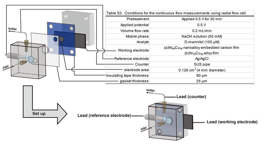
5 Fig. S5 Repeated CVs of (a) Ni 64 Cu 36 nanoalloy embedded carbon film and (b) Ni 70 Cu 30 alloy film obtained in 0.1 M NaOH solution. Red lines correspond to the first cycle and the other cycles are shown as black lines. Interestingly, the peak current of the nanoalloy exhibits a more negative potential and sharp shape than that of the alloy, the values at the 10 th cycle were V for the nanoalloy and V for the alloy. Moreover, the peak area for nanoalloy embedded carbon film at the 10 th cycle (89.1μC cm -2 ) was larger than that of alloy film (83.6 μc cm -2 ) despite the fact that the metal concentration was about 6 times smaller than that of alloy film. These results indicate that the nanoalloys embedded in carbon film have higher electrocatalytic activity than the alloy because more than 7 times the number of homogeneous active sites were formed at the lower potential. Fig. S6 Amperometric detection of D-mannitol obtained with Ni 64 Cu 36 nanoalloy embedded carbon film electrode; NaOHaq, (0.1 M s); D-mannitol (100 μm, s); D-mannitol (100 μm) in the presence of chloride ion (0.2 M, s) S5
6 S6
7 S7