Micromachining vs. Soft Fabrication
|
|
|
- Mark Jefferson
- 5 years ago
- Views:
Transcription
1 Introduction to BioMEMS & Medical Microdevices Silicon Microfabrication Part 1 Companion lecture to the textbook: Fundamentals of BioMEMS and Medical Microdevices, by Prof., R Micromachining vs. Soft Fabrication Microfabrication is the process for the production of devices in the submicron to millimeter range. Micromachining of silicon and other ceramics is similar to integrated circuit fabrication. Soft fabrication techniques include molding, embossing, stamping, casting, thick-film application, self-assembled monolayers (SAMs), and array patterning using polymers and biological substances. Micromachining Materials MEMS devices are made from the same materials used for microelectronics, including: Single crystal silicon wafers. Deposited layers of polycrystalline silicon (polysilicon) for resistive elements. Gold, aluminum, copper and titanium for conductors. Silicon oxide for insulation and as a sacrificial layer (to allow release of moving parts). Silicon nitride and titanium nitride for electrical insulation and passivation. The silicon materials have high strength at small scales which allows higher strain levels and less susceptibility to damage and fracture. 1


2 Soft Fabrication Materials Polymers Surface modification for improved functionality. Hydrogels Environmentally induced changes in shape, size and other attributes. Electroactive Polymers Electrically induced changes in shape, size and other attributes. Biological Materials DNA fragments, biotin labeled albumin, and streptavidin coated polystyrene beads for example. Microelectronics Revolution From Molten Silicon to IC Chips Molten silicon - Czochralski puller technique Silicon wafer diced into integrated circuits (DIP and SMD). Single crystal silicon boule 2
3 Electronic Grade Silicon (EGS) 1. Quartzite is placed in a furnace with carbon releasing materials, and reacts as shown, forming metallurgic grade silicon (MGS): heat Si(s) + 2CO(g) Si0 2(s) + 2C(s) 2. MGS is then treated with hydrogen chloride to form trichlorosilane: Si + 3HCl heat SiHCl (g) + H (g) Next fractional distillation reduction with hydrogen produces electronic grade silicon (EGS): heat SiHCl 3(g) + H 2(g) Si(s) + 3HCl(g) Czochralski Puller Gardner JW et al, Microsensors, MEMS and Smart Devices, John Wiley & Sons, Chichester, NY (2001) Cubic Crystal System (a) SC (b) BCC (c) FCC Crystalline silicon forms a covalently bonded structure and coordinates itself tetrahedrally (bottom). Silicon (and germanium) crystalize as two interpenetrating FCC sublattices. Sze, SM, Semiconductor Devices: Physics and Technology. John Wiley & Sons, New York (1985) 3


4 Miller Indices Madou M, Fundamentals of Microfabrication: The Science of Miniaturization, 2 nd ed. CRC Press, Boca Raton, FL (2002) Surface Micromachining Steps Fatikow S & Rembold U, Microsystem Technology and Microrobotics, Springer, New York (1997) Silicon Wafer Preparation 4


 + O (gas) SiO (solid) and Si (solid) + 2H O (gas) SiO (solid) + 2H (gas) 2 2 2")

5 RCA Cleaning Bench Thermal Silicon Oxide SiO 2 is a silicon atom surrounded tetrahedrally by four oxygen atoms. Structure may be crystalline (quartz) or amorphous (thermal deposition). Gardner JW et al, Microsensors, MEMS and Smart Devices, John Wiley & Sons, Chichester, NY (2001) Thermal Silicon Oxide Methods The chemical reaction that occurs is: C 2 2 Si (solid) + O (gas) SiO (solid) and Si (solid) + 2H O (gas) SiO (solid) + 2H (gas) Dry oxidation at C in pure oxygen produces a better oxide, with higher density than steam oxidation. Thermal silicon oxide is amorphous. Madou M, Fundamentals of Microfabrication: The Science of Miniaturization, 2 nd ed. CRC Press, Boca Raton, FL (2002) 5

azide rubber and Kodak KTFR. Critical Dimension - this is the smallest feature size to be produced.")
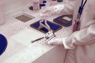
6 Spin-Casting Resist Resist Types Both positive and negative resists can be chosen, depending on whether it is desirable to have the opaque regions of the mask protect the resist, and hence the substrate below, vs. having the transparent regions protect the resist when exposed to UV. Areas where the resist is removed will ultimately be etched. Remember that positive protects. Positive resists include poly(methyl methacrylate) (PMMA), and a two part system, diazoquinone ester plus phenolic novolak resin (DQN). Negative resists include SU-8, bis(aryl)azide rubber and Kodak KTFR. Critical Dimension - this is the smallest feature size to be produced. Resolution smallest line width to be consistently patterned. 6


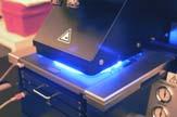

7 Mask Creation UV Exposure at nm Developing the UV Exposed Wafer 7
8 Etching Methods Subtractive processes: Dry etching (plasma), Glow discharge methods (diode setups): Plasma etching (PE), Reactive ion etching (RIE), Physical sputtering (PS). Ion beam methods (triode setups): Ion beam milling (IBM), Reactive ion beam etching (RIBE), Chemical assisted ion beam etching (CAIBE). Deep Reactive Ion Etching (DRIE). Wet etching (chemical liquids). Etching Profiles Isotropic Etching Anisotropic Etching Ziaie B. et al., Hard and soft micromachining for biomems: review of techniques and examples of applications in microfluidics and drug delivery. Advanced Drug Delivery Reviews 56(2), pp (2004). Energy, Vacuum & Directionality Plasma Etching occurs at relatively lower energy and higher pressure (less vacuum), and is isotropic, selective and less prone to cause damage. Reactive Ion Etching is more middle ground in terms of energy and pressure, with better directionality. Physical Sputtering and Ion Beam Milling rely on physical momentum transfer from higher excitation energies and very low pressures, and result in poor selectivity with anisotropic etching and increased radiation damage. 8


9 Plasma Etching (PE) Madou M, Fundamentals of Microfabrication: The Science of Miniaturization, 2 nd ed. CRC Press, Boca Raton, FL (2002) Reactive Ion Etching (RIE) Madou M, Fundamentals of Microfabrication: The Science of Miniaturization, 2 nd ed. CRC Press, Boca Raton, FL (2002) 9
 particles are simply reflected or absorbed. At surface energies between 4-10 ev some surface sputtering occurs.")
10 Physical Sputtering Bombarding a surface with inert ions (e.g. argon) has an effect related to the kinetic energy of the incoming particles. At energies < 3 ev (electron volts) particles are simply reflected or absorbed. At surface energies between 4-10 ev some surface sputtering occurs. At surface energies of ev momentum transfer causes bond breakage and ballistic material ejection across the reactor to the collecting surface. A low pressure and long mean free path are necessary to prevent the material from redepositing. Implantation (doping) occurs at 10,000-20,000 ev. Sputter Yield Sputter yield is the number of atoms removed from the surface per incident ion. Sputter yield depends on the following: Incident ion energy (max yield 5-50 kev). Mass of the ion Mass of the substrate atom to be etched away. Crystallinity and crystal orientation of the substrate. Temperature of the substrate Partial pressure of oxygen in the residual gas. Ion Beam Milling (IBM) Madou M, Fundamentals of Microfabrication: The Science of Miniaturization, 2 nd ed. CRC Press, Boca Raton, FL (2002) 10


11 Reactive Ion Beam Etching and Chemical Assisted Ion Beam Etching RIBE CAIBE Madou M, Fundamentals of Microfabrication: The Science of Miniaturization, 2 nd ed. CRC Press, Boca Raton, FL (2002) Resist Stripping Profilometry 11
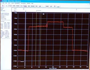
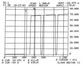

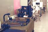
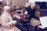
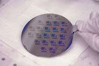
12 Profilometer Screen Display Profilometry Graph Dicing Chips 12


.")
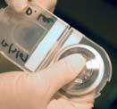
13 Wire Bonding Summary Microfabrication is the process for the production of devices in the submicron to millimeter range. Micromachining of silicon and other ceramics is similar to integrated circuit fabrication. Crystalline silicon forms a covalently bonded structure and coordinates itself tetrahedrally (bottom). Silicon (and germanium) crystalize as two interpenetrating FCC sublattices. 13
14 Surface micromachining concepts discussed: Mask creation, Silicon wafer preparation, Thin-films deposition such as SiO 2, Resist (positive or negative) application, UV exposure and development, Etching methods (substrative processes), Resist stripping, Inspection with profilometer. Dicing and Wire Bonding 14