EE 432/532 CyMOS process PWELL Lithography & Diffusion Feb 24, 2016
|
|
|
- Aubrey Atkinson
- 5 years ago
- Views:
Transcription
1 EE 432/532 CyMOS process PWELL Lithography & Diffusion Feb 24, 2016 Friday Afternoon Group Brady Koht Sebastian Roe Peter Bonnie Joseph Wickner Lab Instructor Yunfei Zhao 1. Overview Now that a Field Oxide was grown in the first lab experiment, it is now time to strategically etch away the oxide and create a p-doped region in the wafers called the PWELL. A layer of photoresist is applied on top of the field oxide. A mask is then placed on top of the photoresist and exposed to UV light. The mask and UV light allows us to strategically place the PWELL region into the silicon. The photoresist exposed to UV light will be removed and the rest of the photoresist will act as a mask for the etching process. In order to deposit and then diffuse a p-type dopant the field oxide needs to be removed. An etch process will remove the field oxide where the photoresist is no longer located. After the field oxide etch the remaining photoresist is removed and diffusion can proceed. A two-step diffusion is used. The first step is to deposit the total dose of boron on to the wafer followed by a drive step to diffuse the boron into a deep p-type region. 2. Photolithography Summarize the steps for patterning and etching using the first mask. Warm Up and Mask Aligner Setup a) Start Mask Aligner and turn on Nitrogen and Air switches for the mask aligner b) Press Power Button and Start the UV lamp c) Clean mask with acetone followed by methanol if necessary Wafer Prime Photoresist Application We will be using a spinner to disperse adhesive promoter and then the photoresist on the wafers. a) Place 2-3/4 diameter chuck on the spinner shaft b) Turn on spinner via Spinner Outlet switch on the top left of the hood i) Should hear vacuum pump begin running c) Use metal tweezers to center the wafer on the chuck d) Place 3-4 Drops of HMDS (hexamethyldisilazane) in center of wafer e) Start Spinner with foot switch, it will automatically shut off f) Fill squeeze dropper half full with photoresist g) Squeeze photoresist onto wafer and start spinner h) Repeat c-g for each wafer Prebake Place photoresist covered wafers into the left oven and prebake them for 25 minutes at º C. 1
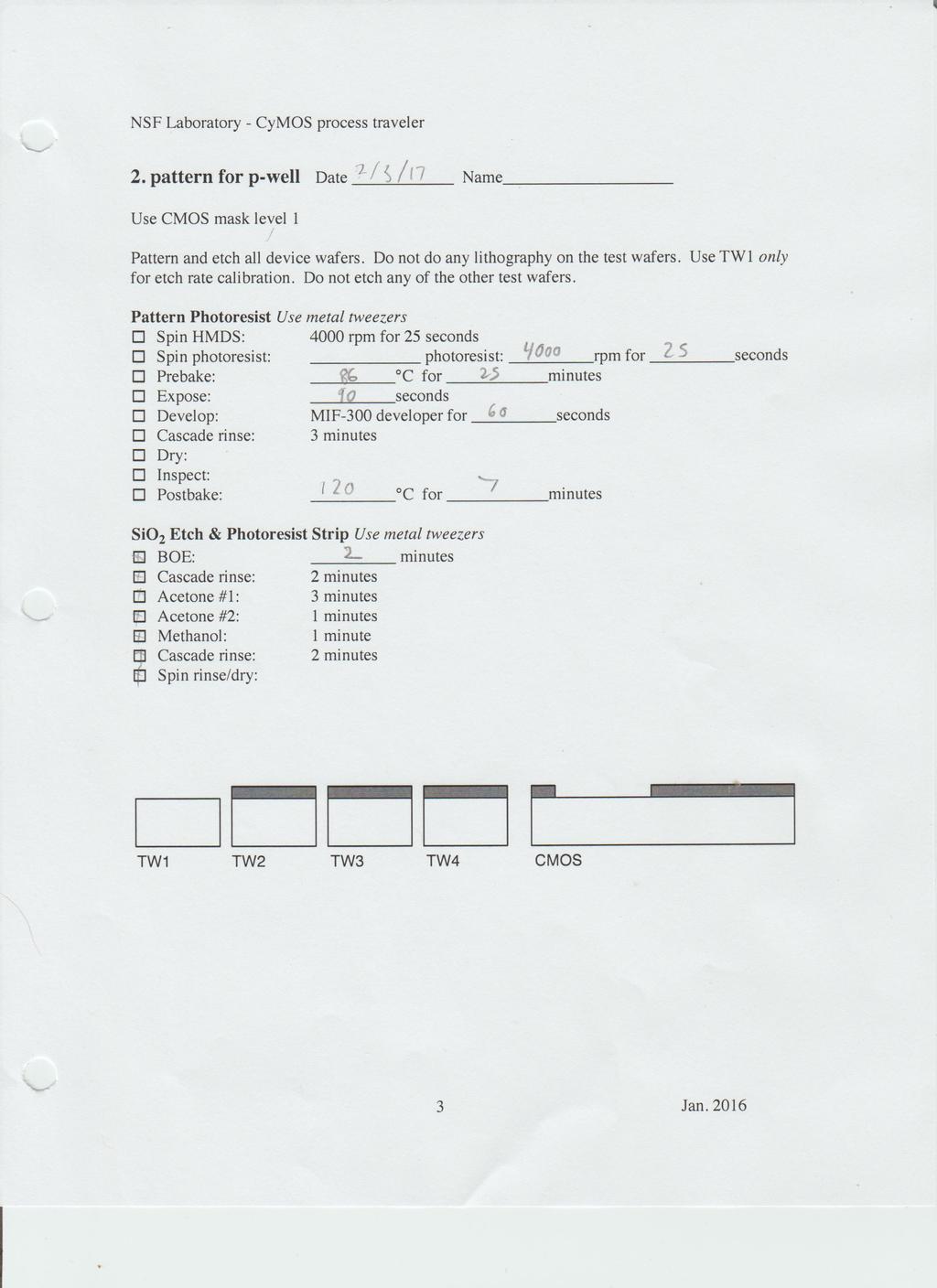
2 Align and Expose Wafer Because this is the first photolithography process completed; the wafer does not need to be aligned to any previously created CyMOS geometry. This greatly simplifies the process. a) Turn on scopes light, select soft contact mode, set scope to one objective b) Place mask on the holder with chrome side facing away and that the vacuum ring is covered. Push vacuum mask button c) Slide mask into the holder and secure using set screws d) Slide out wafer tray and place wafer onto it. Note orientation for future labs e) Slide wafer tray into position under the mask. f) Rotate lever on left side of aligner counter-clockwise to bring mask and wafer into contact. Contact Light doesn t guarantee contact, double check contact. g) Set exposure time (approximately 90 seconds) and start exposure h) After exposure, rotate contact lever clockwise to separate wafer and mask i) Slide wafer tray out and remove wafer. Repeat for additional wafers Develop Photoresist After exposer to the UV light, the exposed photoresist needs to be removed. Revealing the field oxide only in places where we want to deposit boron for the PWELL Deposition steps. a) Fill a deep glass dish with 1cm of MIF-300 developer b) Use metal tweezers to place a wafer into developer c) Agitate for 90 seconds d) Place wafer into wafer carrier then into cascade rinse tub e) Repeat for all wafers f) All wafers need to be in the rinse tub for no less than 3 minutes Inspect and Postbake a) If desired inspect and take photos of wafers using microscope b) Place wafers in oven for 7 minutes at 120 º C Etch Etching step will remove the field oxide that is not covered in photoresist. a) Place Wafer carrier into Buffered oxide etch (BOE) tub b) Use a Test wafer to test for oxide removal i) If water is adhering to wafer (hydrophilic) continue etch ii) If water beads off of wafer (hydrophobic) etch is complete c) Once etch is complete add wafers to cascade rinse tub for 2 minutes Photoresist Strip a) Place Wafers into acetone tub 1 for 3 minutes b) Place wafers into acetone tub 2 for 1 minute c) Place wafers into methanol tub for 1 minute d) Place wafers into cascade rinse tub for 2 minutes e) Rinse and dry wafers with spin rinser/dryer 2
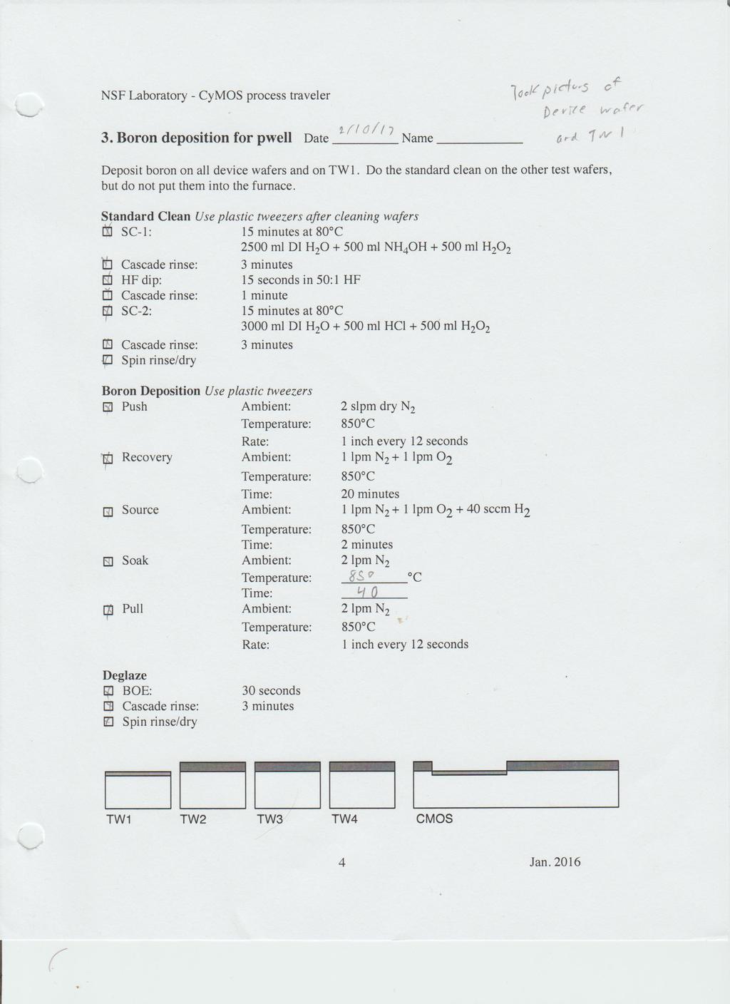
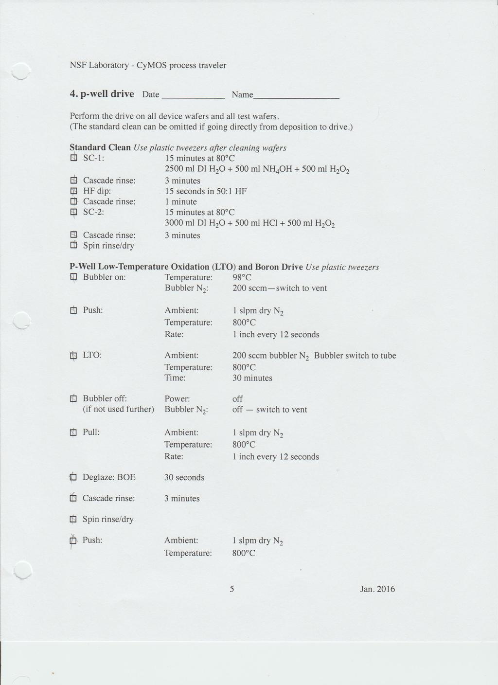
3 3. Boron deposition and drive Standard Clean The standard clean process is used to rid the surface of the wafers of any contaminants that could interfere or ruin the operation of the final semiconductor device. A brief synopsis of the steps in the standard clean process are listed below. a. The wafers are left in a tub of 2500 ml of DI water, 500ml of ammonium hydroxide (NH4OH), and 500 ml of hydrogen peroxide (H2O2) at 75 º C for 15 minutes. b. The wafers are then put into the cascade rinse tub consisting of DI water and constant nitrogen flow that agitates the water for 3 minutes c. The wafers are then loaded into the diluted hydrofluoric acid (HF) tub for 15 seconds before being added to the cascade rinse again for another minute. d. The wafers are then washed in a tub of 3000 ml of DI water, 500 ml of hydrochloric acid (HCl), and 500 ml of hydrogen peroxide (H2O2) for 15 minutes. e. Wafers are then put back in the cascade rinse tub for 3 minutes. f. To end the standard clean process, the wafers are then rinsed and dried in the spin rinse and dryer. Boron Deposition The purpose of the boron deposition is to set the initial dose for the 2 step diffusion process. a. Remove the wafer boat and prepare to load wafers onto the boat b. Set the temperature to 850 º C and set nitrogen to 2 slpm c. Load wafers with side to be doped facing source wafers d. Push boat to center of furnace at rate of 1 inch every 12 seconds e. Set oxygen flow to 1 slpm and decrease nitrogen to 1 slpm for 20 minutes f. After those 20 minutes open and flow hydro gen at 40 sccm for 2 minutes g. Shut off oxygen and increase nitrogen back to 2 slpm h. Leave wafers in furnace for calculated soak time i. Remove wafers at rate of 1 inch every 12 seconds j. bring furnace down to 400 º C and nitrogen to.3 slpm Deglaze a. Put wafers in Buffered Oxide Edge for 30 seconds b. Cascade rinse wafers for 3 minutes c. Spin rinse/dry cycle using the spin rinser The calculations for the soak time are located in the appendix below. Low Temperature Oxidation a. Bring furnace tube 3 to 800 º C with 1 slpm of nitrogen b. Fill bubbler with DI and start nitrogen flow through bubbler to 200sccm c. Bubbler should be set to 98 º C and takes 15 minutes to heat up d. Load the wafers on to the boat with guard wafers on each end of the boat e. Push the boat into the furnace at a rate of 1 inch every 12 seconds f. Turn off dry nitrogen flow and flip vent bypass switch to TUBE g. Wait for 30 minutes. 3

4 Deglaze a. Put wafers in Buffered Oxide Edge for 30 seconds b. Cascade rinse wafers for 3 minutes c. Spin rinse/dry cycle using the spin rinser Oxidation and Drive a. Reload the wafers into the furnace b. Ramp the temperature to 1150 º C and refill bubbler if needed c. Turn off nitrogen flow and turn vent bypass switch to TUBE d. Wet Oxidation will last for 10 minutes e. Turn off bubbler and set nitrogen to 1 slpm f. Leave wafers in furnace for 12 hours and 50 minutes for the drive g. Ramp furnace down to 800 º C h. Pull wafers at 1 inch for every 12 seconds 4. Results Below are 3 of the several pictures taken after the PWELL Lithography lab. The pictures depict the results of the photoresist development process. Which shows very solid and straight lines without much if any distortion of the mask image. 4
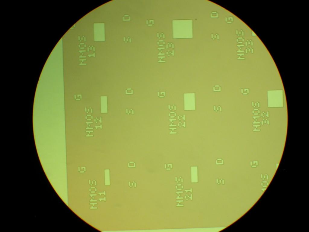
5 5


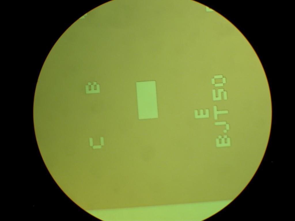
6 The two pictures below are of a Device wafer one after the oxide etch and the photoresist strip process. The second photo shows the great amount of detail in the mask and oxide etch. 6

7 The last picture is of test wafer one after the oxide etch and photoresist strip. 7
8 5. Appendix Givens: Boron D0 = 1 cm 2 /s EA = 3.5 ev Solid State 800 º C = 7x10 19 cm 900 º C = 1.2x10 20 cm -3 Furnace Temperature = 850 º C Thus Solid State 850 º C = 1.2xx1020 7xx xx10 19 = 9.5xx10 19 cm -3 2 Using the given values: DD = DD 0 exp EE AA = 1.959xx10 16 KKKK Now we need to solve the below equation for the time t. We know a range of doses (Q) given from the lab at 7.5x10 13 to cm -2. These are our upper and lower limits. We have already solved for D and we solved for Ns as the solid solubility 850 º C which is 9.5xx10 19 cm -3. QQ = 2NN ss ππ DDDD 7.5x10 13 = 2 9.5xx1019 cm xx10 16 tt ππ Solving for t= minutes at the lower dose limit. And if we solve at the higher limit t = minutes. So we opted for a drive time of 40 minutes. While this may seem like a not enough time given out lower limit dose time. The deposition process is still occurring during the time it takes to pull the wafer boat out of the oven. It takes approximately 5 minutes to remove the boat putting us into our soak time range. 8
9
10
11

12