New approaches to classical Silicon Solar Cells
|
|
|
- Maurice O’Connor’
- 5 years ago
- Views:
Transcription
1 New approaches to classical Silicon Solar Cells The SSTEP Project Solar-grade Silicon by Transfer and EPitaxy G.Amato - INRIM, Torino G. Borionetti- MEMC, Novara
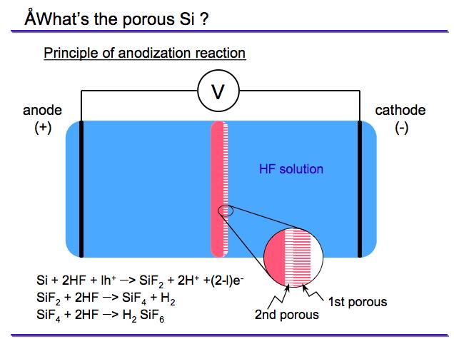
2 Contents 1. What s the porous Si? 2. Epitaxy 3. ELTRAN vs. SSTEP processes 4. Photonics in SSTEP 5. Summary
3
4
5
6
7 Epitaxy CVD is the most common method of Si epitaxy Reduction of chlorosilanes(sicl4, SiHCl3, SiH2Cl2, SiH4) at high temperature (~ 900 C C), e.g. SiHCl3 (v) + H2(v) Si (s) + 3HCl (v) Hydrogen is used as reducing agent and carrier gas. The reaction is surface catalyzed. SiHCl3and SiH2Cl2 are typical silicon sources Good balance between safety and process needs in atmospheric conditions Today, TCS is the preferred source (liquid at RT) requires medium high deposition temperature SiCl4requires too high deposition temperature SiH4 is used when a low transition region or no pattern shift is requested. Very low deposition temp (900 C) but more difficult to manage than TCS.
8 Epitaxy Diffusioncontrolled Kinetic-controlled From: W.R.Runyan, K.E.Bean, Semiconductor Integrated Circuit Processing Technology 1994, pg. 317

9 Epitaxy Doping The dopant is co-deposited with silicon. Epi dopant and resistivity: type P: B (B2H6) -> ohm*cm type N: P (PH 3 ) As (AsH 3 ) Ωcm Substrate dopant and resistivity: type P++: B -> 2-5 mohm*cm type P+: B -> 8-20 mohm*cm type P-: B -> >1 ohm*cm type N++: As,Red-P ->1-5 mohm*cm type N+: Sb-> mohm*cm
10 Epitaxy
11
12 SSTEP glueing Glass.. Plastics Doping p/n junction
13 SSTEP
14 SSTEP Y is the SSTEP wafer cost H is the price of the handle substrate S is the price of the seed wafer R is the price of reclaiming the seed wafer N is the number of times the seed wafer is re-used As n increases Y-> H+R
15
16
17
18 SSTEP
19 SSTEP Photonics
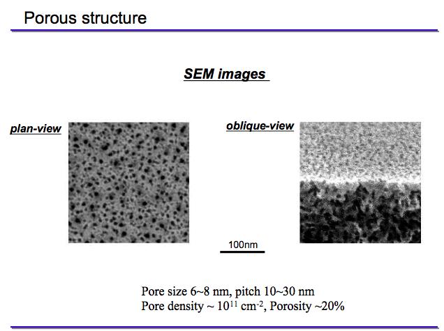
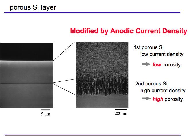
20 Photonics Porosity Current density (ma/cm2) Porosity Refractive Index Time Careful! The etch rates are not the same! Depth Current density (ma/cm2) Refractive Index


21 Photonics nd=λ/4 High n Low n nd=λ/4 nd=λ/2 Reflectivity Wavelength (nm) Reflectivity Wavelength (nm)

22 Photonics Antireflective coating Reducing the index step at the Air-Si interface

 http://www-user.riec.")
23 Photonics Photonic crystals Obtained using IC s technologies Stack of semiconductors stripes (asymmetric fcc structure) Si (SiO2) III-V Corrugated multilayers Hanaizumi et al. APL. 74 (1999)


24 Photonics Hexagonal array of holes (a = 1µm) obtained by e-beam lithography


25 Photonics Side view of the non patterned area e/2 Side view of the patterned area

26 Photonics Removal of the layer Etching with the current modulation...


27 Photonics New wave Structure Representation of the refractive index changes


28 Photonics Coherent porosity modulations No limitation of the number of periods: here 35 Non patterned area
29 Photonics 3 beam interference λ= 488 nm Min period = 244 nm
30 Conclusions SSTEP is: -reliable (it derives from the ELTRAN process) -flexible -> thickness of the Epi-layer corrugation of the Epi-layer antireflective coatings 1D to 3D photonics -cheap (Y-> R+H) -needs for financial support (no Martini, no party )