DEVICE BEHAVIOR OF CZTSE/SI NANOWIRE HETEROJUNCTION
|
|
|
- Lewis Peters
- 5 years ago
- Views:
Transcription
1
2
3
4
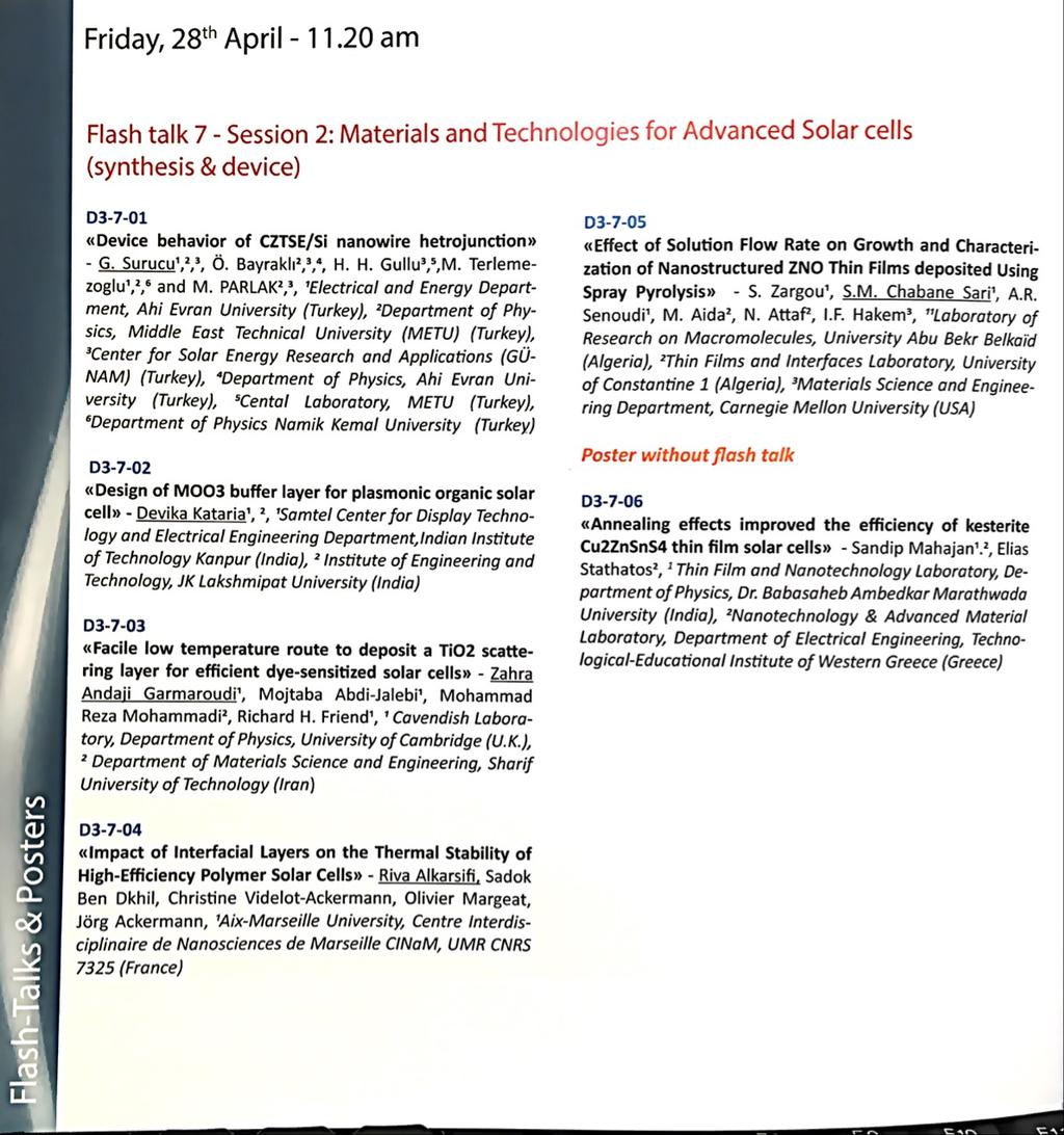
5 PHOTOVOLTAIC TECHNICAL CONFERENCE - FROM ADVANCED MATERIALS AND PROCESSES TO INNOVATIVE APPLICATIONS DEVICE BEHAVIOR OF CZTSE/SI NANOWIRE HETEROJUNCTION G. Surucu 1,2,3, Ö. Bayraklı 2,3,4, H. H. Gullu 3,5, and M. PARLAK 2, 3 1 Electrical and Energy Department, Ahi Evran University, 40100, Kirsehir, TURKEY 2 Department of Physics, Middle East Technical University (METU), 06800, Ankara, TURKEY 3 Center for Solar Energy Research and Applications (GÜNAM), METU, Ankara, Turkey 4 Department of Physics, Ahi Evran University, 40100, Kirsehir, TURKEY 5 Cental Laboratory, METU, Ankara, TURKEY 1) Context / Study motivation Current research trends are moving towards earthabundant and low toxicity materials. Copperindium-gallium-selenide (CIGS) and cadmium telluride (CdTe) are two leading thin film solar technologies that have already been commercialized. Despite several advantages already reported in the literature for CdTe films [1], cadmium is toxic and tellurium is rare. CIGS thin films also have disadvantages similar to those of cadmium telluride. Selenium is a toxic material and gallium and indium are not abundant [2,3]. In contrast, the elemental constituents of Cu2ZnSnS4 (CZTS) are not only earth-abundant, but also nontoxic, which makes CZTS a very attractive candidate for the fabrication of solar cells on a large scale. Furthermore, CZTS has a band gap of 1.5 ev and an absorption coefficient of about 104 cm-1, optimum values for thin film solar cells [4,5]. 2) Description of approach and techniques fabricate vertically oriented Si nanowires on n-type (111) mono-crystalline 600 µm Si wafers with the resistivity value of 1-3 (Ω.cm). In this etching process, the lengths of the n-type Si nanowires were controlled by the etching time, and so that three different Si wafer substrates were prepared with about 1.75, 3.0 and 6.0 nm nanowire lengths. The heterojunction diodes were constructed by depositing 600 nm p-cztse thin film layer using physical vapor deposition technique onto these fabricated Si nanowires. Thin film deposition was also carried out on commercial soda lime glass substrates at the same condition. Initially, the structural and optical properties of the CZTSe thin film deposited on the glass substrates were analyzed. Then, detailed electrical characterization of these heterojunction diodes were performed by the help of current-voltage (I-V) (dark and under illimination conditions) and capacitance-voltage (C-V) measurements to understand their electrical properties depending on length of the nanowire on Si substrate. In this work, electrical properties of p-cztse/n-si nanowire heterojunction diodes were investigated depending on the nanowire lengths. Metal-assisted etching method performed by AgNO3 and HF solution at different etching times was applied to 3) Results / Conclusions / Perspectives The fabricated diodes exhibited rectifying characteristics and from these I-V measurements, the advantages of the nanowire geometry compared to reference device were discussed based on the calculated device parameters. The change in device
) -14-16 Figure-3: SEM image for Si nanowires on Si wafers -18-20 illimunated dark -1.5-1.0-0.5 0.0 0.5 1.")


6 parameters such as Rs, Rsh, the diode ideality facor n and barrier heights with the illumination were analyzed. C-V measurements were carried out for different frequencies. The device behavior due to the different frequencies was also studied n30-12 Ln(I(A)) Figure-3: SEM image for Si nanowires on Si wafers illimunated dark V(V) REFERENCES: Figure-1: Ln(I) vs. V graph under dark and illumination conditions for p-ctzse/n-si nanowire 1. Wu X. High-efficiency polycrystalline CdTe thin-film solar cells. Solar Energy 2004;77 : Jimbo K, Kimura R, Kamimura T, Yamada S, Maw WS, Araki H, Oishi K, Katagiri H. Cu2ZnSnS4-type thin film solar cells using abundant materials. Thin Solid Films 2007;515 : Tanaka K, Oonuki M, Moritake N, Uchiki H. thin film solar cells prepared by non-vacuum processing. Solar Energy Materials and Solar Cells 2009; 93 : Schubert B, Marsen B, Cinque S, Unold T, Klenk R, Schorr S, Schock H. Cu2ZnSnS4 thin film solar cells by fast coevaporation. Progress in Photovoltaics: Research and Applications 2011; 19 : Ennaoui A, Lux-Steiner M, Weber A, Abou-Ras D, Kötschau I, Schock H-, Schurr R, Hölzing A, Jost S, Hock R, Voß T, Schulze J, Kirbs A. Cu2ZnSnS4 thin film solar cells from electroplated precursors: Novel low-cost perspective. Thin Solid Films 2009; 517 : Figure-2: Frequency dependent C-V measurements for p- CTZSe/n-Si nanowire


Se 2 (CIGS) thin film based solar cells are pushing %21.7 efficiency and this explains the increasing popularity[1].")
 thin films [2,3].")
7 PHOTOVOLTAIC TECHNICAL CONFERENCE - FROM ADVANCED MATERIALS AND PROCESSES TO INNOVATIVE APPLICATIONS DEPOSITION AND CHARACTERIZATION OF ZTSES THIN FILMS FOR PHOTOVOLTAIC APPLICATIONS Ö. Bayrakl1 1,2,3, H. H. Gullu 2,4, M. Terlemezoglu 1,2,5 G. Surucu 1,2,6 and M. PARLAK 1,2 1 Department of Physics, Middle East Technical University (METU), 06800, Ankara, TURKEY 2 Center for Solar Energy Research and Applications (GÜNAM), METU, Ankara, Turkey 3 Department of Physics, Ahi Evran University, 40100, Kirsehir, TURKEY 4 Cental Laboratory, METU, Ankara, TURKEY 5 Department of Physics Namik Kemal University, 59030, Tekirdag, Turkey 6 Electrical and Energy Department, Ahi Evran University, 40100, Kirsehir, TURKEY 1) Context / Study motivation The importance and demand of thin film solar cells are getting higher among photovoltaic industry. As thin film amorphous silicon is at %14 efficiency levels, Cu(In,Ga)Se 2 (CIGS) thin film based solar cells are pushing %21.7 efficiency and this explains the increasing popularity[1]. However, the current downside of these cells is the ingredient elements requiring extensive and large scale production. Many solar cells and optoelectrical devices in the applications involve ZincIindium Selenide (ZnIn2Se4) thin films [2,3]. ZnIn 2 Se 4 is an n-type ternary chalcogenide semiconductor of type A I B II X IV, where A=Zn, Cd, or Hg, B=In or Ga, and X=Se, S, Te [4,5]. Zn or Sn which belong earth abundant elements category, can be used instead of In and Ga which are rare elements. 2) Description of approach and techniques In this study, ZnSn(Se,S) (ZTSeS) thin films will be deposited with e-beam and sputtering techniques which are two types of the physical vapor deposition techniques. In order to get the information about the effects of the postannealing, heat treatment at C under N atmosphere was applied. Then structural, optical and electrical properties of as grown and annealed films were investigated. For structural characterization; X-ray diffraction (XRD), Scanning Electron Microscopy (SEM), Energy Dispersive X-ray Analysis (EDS) and Raman measurements were done. Then, for optical characterization; transmission and reflection measurements were performed. Finally, temperature dependent photoconductivity and Hall Effect measurements were carried out to obtain electrical characterization. 3) Results / Conclusions / Perspectives As seen from Figure-1 films have better crystal structure with the annealing. The band gap values are found as 1.35 ev for the films. Activation energies are obtained as 23 mev and 14 mev for high temperature and low temperature regions respectively. Figure-1: XRD patterns for asgrown and annealed ZTSeS thin films. Table-1: EDS results for asgrown and annealed ZTSeS thin films. a)
 asgrown ZTSeS and (b) annealed ZTSeS thin films.")

![REFERENCES: [1] P. Jackson, D. Hariskos, R. Wuerz, O. Kiowski, A. Bauer, T. M.](/docs-images/93/112457806/images/8-2.jpg "Friedlmeier, M. Powalla P hys. Status Solidi RRL 9 (2015) 28. [2] F.J. Gracia, M.S. Tomar, Thin Solid Films 69 (1980) 137.")
![[3] J. Fillpowicz, N. Romeo, L. Tarricone, Solid State Commun. 38(1980)619. [4] L.](/docs-images/93/112457806/images/8-3.jpg "Gastaldi, M.G. Simcon, S. Vitivoli, Solid State Commun. 55 [5] J.A. Buan, R.")
8 b) Figure-2: (αhν) 2 vs. hν graphs for (a) asgrown ZTSeS and (b) annealed ZTSeS thin films. Figure-3: Temperature dependent photoconductivity measurements for asgrown and annealed ZTSeS thin film under different illumination intensities. REFERENCES: [1] P. Jackson, D. Hariskos, R. Wuerz, O. Kiowski, A. Bauer, T. M. Friedlmeier, M. Powalla P hys. Status Solidi RRL 9 (2015) 28. [2] F.J. Gracia, M.S. Tomar, Thin Solid Films 69 (1980) 137. [3] J. Fillpowicz, N. Romeo, L. Tarricone, Solid State Commun. 38(1980)619. [4] L. Gastaldi, M.G. Simcon, S. Vitivoli, Solid State Commun. 55 [5] J.A. Buan, R. Nitsche, M. Lichtensteiger, Physica 27 (1961) ) 605.