Transzmissziós és pásztázó elektronmikroszkópos minták készítése ionsugaras vékonyítással
|
|
|
- Franklin McKinney
- 5 years ago
- Views:
Transcription


1 Transzmissziós és pásztázó elektronmikroszkópos minták készítése ionsugaras vékonyítással Radi Zsolt Technoorg Linda Kft., Budapest Oktatói és Doktorandusz Konferencia Visegrád, 2012


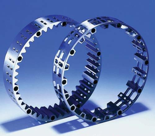
2 State-of-the-art materials


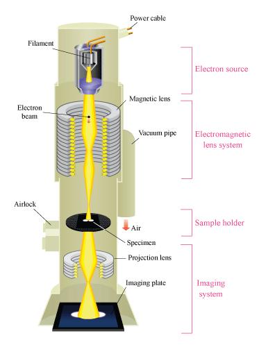
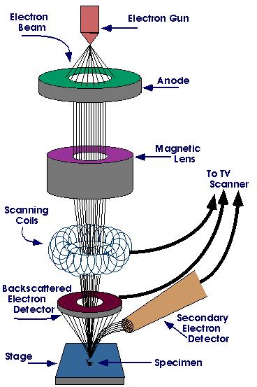
3 SEM TEM - FIB
4 TEM/SEM preparation flow Bulk Specimen / Surfaces SEM or Plan View in TEM Interfaces / Thin Films Cross Section in TEM Bulk Reduction (~ 1cm size) Wire Saw Diamond Wheel Saw Acid Saw Band Saw Cleaving Ultrasonic Cutter Specimen Mounting Bulk Reduction (< 1mm size) Wire Saw Diamond Wheel Saw Acid Saw Band Saw Cleaving Disc Cutter Embedding (e.g., 3mm disc) Slope Cutting Surface Etching or Cleaning Initial Thinning (< 200μm) Final Thinning (< 100nm) Dimpling Tripod Polishing Electropolishing / Chemical Polishing Ultramicrotomy Ion milling FIB


5 Mechanical pretreatment Raw sample sectioning with the MICROSAW diamond saw Sample encapsulation into a TITANIUM disc using the MICROHEAT heated table and the AT1 special glue Sample dimpling and/or polishing with the MICROPOL grinder and polisher


6 Scanning electron microscopy applications ion beam workstation for SEM sample preparation: rapid slope cutting and gentle surface cleaning ion energy range: ev and ev
7 Sputtering rate of Si at LEG - focused low-energy ion source Ultra-high-energy ion milling Sputtering rate ( µm/hour) HEG - standard high-energy ion source FHEG - focused high-energy ion source Low-energy sample trimming Sample cleaning Conventional highenergy ion milling Ion energy (ev)
 Compact design and small size (ø 55 mm) Compatible with most")

8 TeleTwin high-energy ion gun (Ar) Broad range of ion energies ( ev) High beam current and current density (150 µa, 50 ma/cm 2 ) Compact design and small size (ø 55 mm) Compatible with most noble gases (Ne, Ar, Xe) Full electronic control of source parameters Suitable for TEM sample preparation, slope cutting, patterning and analytical depth profiling Ideal for standard ion beam applications
9 Sputtering rate of Si at LEG - focused low-energy ion source Ultra-high-energy ion milling Sputtering rate ( µm/hour) HEG - standard high-energy ion source FHEG - focused high-energy ion source Low-energy sample trimming Sample cleaning Conventional highenergy ion milling Ion energy (ev)

10 Dedicated low-energy ion gun (Ar + ) Extremely low ion energies ( ev) High beam current and current density (80 µa, 5 ma/cm 2 ) Ultra-low size (ø 35 mm) Full electronic control of source parameters Suitable both for highquality sample preparation and analytical depth profiling Ideal for special ion beam applications


11 Designed to produce planar cross-sections of solid state materials for SEM imaging and microanalysis: Zn coated steel, cut made at slope angle of 45º into the near-surface layer of a bulk sample


")
 positioning")
12 Sample stage for ion beam slope cutting and cut plane cleaning in-plane motion (oscillation) tilting (in 0-30 range) positioning (with 1µm accuracy)
 study and orientation imaging microscopy (OIM): Inverse Pole Figure (IPF) of a polycrystalline copper wire")
13 weak halo pattern of the intense central beam part Ar ion beam sample holder (top view) intense central part pattern of the weak halo Ar ion beam ion source ion source Designed to produce samples for electron back scatter diffraction (EBSD) study and orientation imaging microscopy (OIM): Inverse Pole Figure (IPF) of a polycrystalline copper wire sample


14 Sample stage for ion beam surface cleaning in-plane motion (rotation) tilting (in 0-30 range) vertical positioning EBSD applications OIM application surface analytics
15 TEM sample preparation Complete sample preparation process from cutting the bulk material to cleaning the TEM samples with lowenergy ion beam Mechanical pretreatment Ion beam thinning ( ev) max. 80 µm thick flat samples (sputtering time limited) max. 150 µm thick dimpled samples Ion beam trimming and cleaning ( ev) trimming of TEM samples prepared in other ion mills low-energy cleaning of TEM samples prepared in other ion mills or FIB columns
16


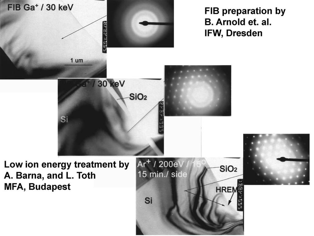
17 Á. Barna, G. Radnóczi and B. Pécz in Handbook of Microscopy, VCH Verlag, Vol. 3, Chapter II/3, (1997)


18 Transmission electron microscopy applications dedicated low-energy ion beam workstation for TEM/FIB sample preparation ion energy range: ev


")
19 Sample stage for ion milling, trimming and cleaning of TEM samples dedicated low-energy ion beam workstation for TEM/FIB sample preparation beam energy beam current beam shape in-plane motion (rotation) in-plane motion (oscillation) tilting (in 0-45 range)
20 Sputtering rate of Si at LEG - focused low-energy ion source Ultra-high-energy ion milling Sputtering rate ( µm/hour) HEG - standard high-energy ion source FHEG - focused high-energy ion source Low-energy sample trimming Sample cleaning Conventional highenergy ion milling Ion energy (ev)
 TEM.")
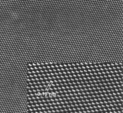
21 Quality Improvement Due to Reduced Energy of Ion Bombardment HRTEM images of GaAs obtained by a Philips CM20 (TWIN) TEM. Sample thinned by Ar + ions at 3000 ev (a) and 200 ev (b).
 and low-angle (3 ) ion")
![milling. Dumbbells in Si [110].](/docs-images/93/112951302/images/22-4.jpg "Sample prepared at Berkeley Lab, CA, USA by Technoorg")
22 Quality Improvement Due to Reduced Energy of Ion Bombardment Low-energy (200 ev) and low-angle (3 ) ion milling. Dumbbells in Si [110]. Sample prepared at Berkeley Lab, CA, USA by Technoorg Linda s low-energy ion source.


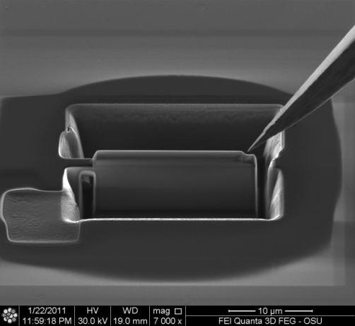
23 FIB samples
24

25 Thank you for the attention.
26 Artifacts developing during ion beam erosion surface roughening preferential sputtering alteration separation ion V < V < 3 V < V V 1 V 2 V 3 V4 A,B compound V > V A B B amorphisation stress, etc. mixing damaged layer void stress ion A B A B sample temperature during ion beam thinning ( damage by sample fabrication )
27 30 kev
28 Artifacts developing during ion beam erosion surface roughening preferential sputtering alteration separation ion V < V < 3 V < V V 1 V 2 V 3 V4 A,B compound V > V A B B amorphisation stress, etc. mixing damaged layer void stress ion A B A B sample temperature during ion beam thinning ( damage by sample fabrication )


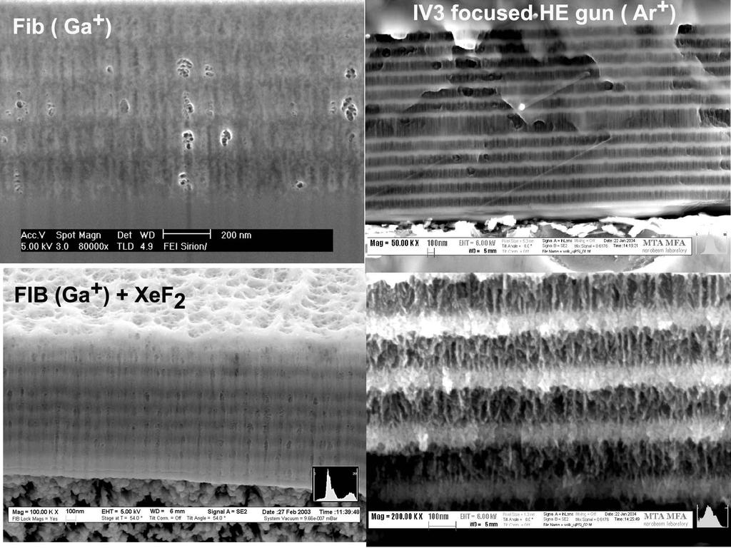
29 Surface roughening due to sputtering rate differences
30 Artifacts developing during ion beam erosion surface roughening preferential sputtering alteration separation ion V < V < 3 V < V V 1 V 2 V 3 V4 A,B compound V > V A B B amorphisation stress, etc. mixing damaged layer void stress ion A B A B sample temperature during ion beam thinning ( damage by sample fabrication )


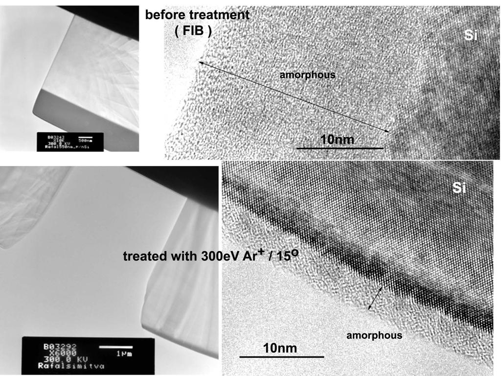
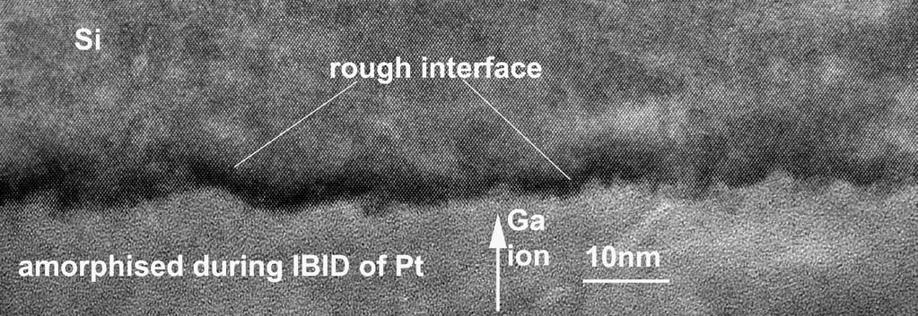
31 High resolution image taken on the Si sample after FIB preparation. Thick amorphous coverage is evident from the image taken at the edge of the sample. High resolution image taken on the above sample after low energy Ar ion bombardment. The damage is reduced substantially.
32
33 Artifacts developing during ion beam erosion surface roughening preferential sputtering alteration separation ion V < V < 3 V < V V 1 V 2 V 3 V4 A,B compound V > V A B B amorphisation stress, etc. mixing damaged layer void stress ion A B A B sample temperature during ion beam thinning ( damage by sample fabrication )
34
35 Artifacts developing during ion beam erosion surface roughening preferential sputtering alteration separation ion V < V < 3 V < V V 1 V 2 V 3 V4 A,B compound V > V A B B amorphisation stress, etc. mixing damaged layer void stress ion A B A B sample temperature during ion beam thinning ( damage by sample fabrication )


36 Liquid Nitrogen Cooling System