This document is downloaded from DR-NTU, Nanyang Technological University Library, Singapore.
|
|
|
- Earl Barker
- 5 years ago
- Views:
Transcription
1 This document is downloaded from DR-NTU, Nanyang Technological University Library, Singapore. Title Author(s) Citation Effect of post-reflow cooling rate on intermetallic compound formation between Sn 3.5 Ag solder and Ni P under bump metallization He, Min; Chen, Zhong; Qi, Guojun; Wong, Chee C.; Mhaisalkar, Subodh Gautam He, M., Chen, Z., Qi, G., Wong, C. C., & Mhaisalkar, S. G. (2004). Effect of post-reflow cooling rate on intermetallic compound formation between Sn 3.5 Ag solder and Ni P under bump metallization. Thin solid films, , Date 2004 URL Rights 2004 Elsevier. This is the author created version of a work that has been peer reviewed and accepted for publication by Thin Solid Films, Elsevier. It incorporates referee s comments but changes resulting from the publishing process, such as copyediting, structural formatting, may not be reflected in this document. The published version is available at: [
2 Effect of Post-Reflow Cooling Rate on Intermetallic Compound Formation between Sn-3.5Ag Solder and Ni-P Under Bump Metallization Min He a, Zhong Chen a, Guojun Qi b, Chee Cheong Wong a, Subodh Mhaisalkar a a School of Materials Engineering, Nanyang Technological University, Singapore b Singapore Institute of Manufacturing Technology, 71 Nanyang Drive, Singapore Abstract Cooling rate is an important parameter in solder reflow process because it influences not only microstructure of solder alloy but also the morphology and growth of intermetallic compounds (IMC) formed between solder and its metallization. All these ultimately affect the mechanical integrity of the joint. In this work, the effect of cooling rate on IMC growth is studied in Sn-3.5Ag solder/ni-p UBM system. Morphology and growth kinetics of the formed Ni 3 Sn 4 IMC under different cooling rates are studied. Needle-type, boomerang-type and chunk-type of Ni 3 Sn 4 IMCs have been observed between solder and Ni-P UBM under various cooling conditions. The amount of the needle-type and boomerang-type grains decreases with the increase of reflow time. Prolonged reflow results in continuous layer of chunk-type IMC grains with no obvious effect from the cooling rate. Samples with different post-reflow cooling rate are further annealed. It is found that the IMC layer thickness increases faster in samples under fast cooling rate than the slow ones under the same annealing condition. Keywords: Lead-free solder, Reflow, Electroless nickel, Intermetallic compound Corresponding author. Tel.: ; Fax: address: aszchen@ntu.edu.sg (Z.Chen)
3 1. Introduction Formation of Ni 3 Sn 4 intermetallic compounds (IMC) layer is the direct result of reaction between Sn-based solders and Ni-P under bump metallization (UBM) [1, 2]. IMC formation is the prevalent mechanism in making permanent solder bonds. However, because of IMCs brittle nature and the difference in mechanical, thermal and electrical properties between IMC and adjacent materials, too thick IMC would lead to adverse effect on the reliability of a solder joint [3, 4]. In a soldering reflow temperature profile, post-reflow cooling rate is an important parameter. The cooling requires being sufficiently slow to prevent thermal shock damage to the packaging and substrate materials. However, an excessively slow cooling rate may unnecessarily lengthen the fabrication process [5]. Therefore an appropriate cooling rate has to be chosen. Meanwhile cooling rate affects the microstructure of both bulk solder and the intermetallic compounds layer at the interface, which in turn affects the reliability of the solder joint. There have been some reports about cooling rate effect on eutectic SnPb solder and lead-free solders [6-9]. Some have focused on the microstructure of the bulk solders, and the joint reliability was evaluated by a mechanical test. Less attention has been paid to the influence of cooling rate on the morphology and growth of the IMC. The main objective of this paper is to study the cooling rate effect on the morphology and growth kinetics of the IMC formed between Sn-3.5Ag and Ni-P UBM during both liquid state reaction and solid state reaction. 2. Experimental procedures The substrates used in this study were prepared from blank Si wafers. A chromium layer (
4 μm), which provides good adhesion of the UBM to the wafer, was sputtered first, followed by a layer of sputtered nickel (1 m). A thin layer of gold was then sputter-coated on the nickel surface to protect under layers from oxidation. Ni-P UBM layer was obtained by electroless plating on the sputtered nickel substrate. Before the plating, the sputtered gold layer was etched away. After reaching a thickness of about 5 m, Ni-P plating process was stopped and a final finish by immersion gold was applied as a surface protection. The lead-free Sn-3.5Ag solder used was in the form of wire with no-clean reflow flux in the core. In the reflow process, the solder wire was placed onto the Ni-P UBM prepared as the above procedure and then sent into a reflow oven. Three thermocouples were used to monitor the temperature change during reflow process. The temperature profiles were controlled such that the solder was heated at the rate of 2.5 o C/s to a peak temperature of 251 C (30ºC above the melting temperature of Sn-3.5Ag solder) and held for 30s, 180s and 600s. Then samples were cooled in oven, air or quenched in water with cooling rate 0.35ºC/s, 3.0ºC/s and 45ºC/s (hereafter referred to as slow, medium and fast cooling rate), respectively. The cooling rate was calculated in the temperature range from melting point to 30ºC below the melting point. Selected Sn-3.5Ag solder samples reflowed for 180s with different cooling rates were annealed at 150 C and 170 C for 100, 225, 400, 625 and 900 hours. Reflowed and annealed samples were prepared for observations on the cross sectional structure and top view of the IMC morphology under SEM. The common metallography practice was followed to reveal the cross sectional view. In order to observe top view of intermetallic compounds, majority of the solder was ground away first, followed by etching in 2% HCl to dissolve the remaining solder. Image analysis software was used to measure the area - 3 -
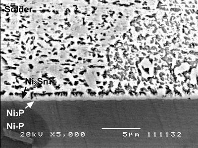
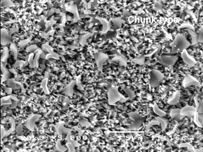
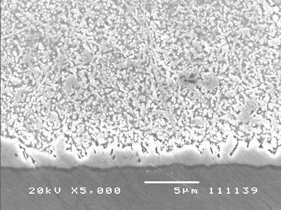
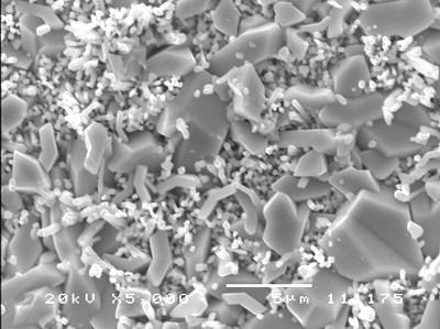
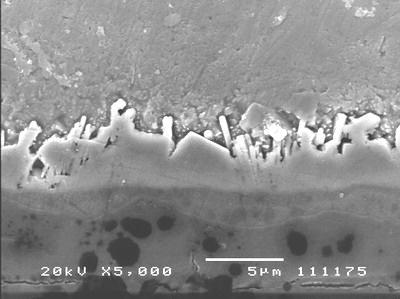
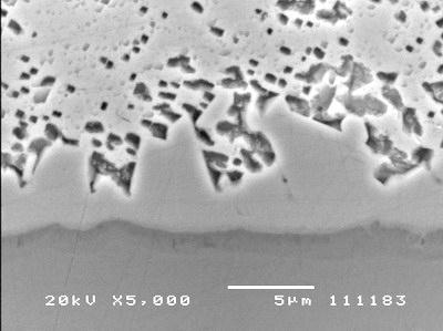
5 and length of IMC in cross sectional SEM images. The average thickness of IMC layer was calculated using measured area divided by length in the area. Each sample was measured more than 10 locations. 3. Results 3.1. Morphology of Ni 3 Sn 4 intermetallic compounds under different cooling rates Top structural and cross sectional SEM micrographs of Ni 3 Sn 4 intermetallic compounds in Sn-3.5Ag/Ni-P UBM system reflowed for 30 s at 251 o C then cooled in three different cooling rates are shown in Fig. 1. EDX and XRD analysis confirm that the IMC formed between solder and Ni-P UBM is Ni 3 Sn 4. There is an additional layer, which consists of Ni 3 P, in between the Ni 3 Sn 4 IMC and Ni-P UBM layers. These observations agree with existing work on Ni-solder reaction [10-12]. From the top view of SEM micrographs as shown in Fig. 1(a), (c) and (e), three types, namely chunk-type, boomerang-type and needle-type, of Ni 3 Sn 4 morphology are observed in all Sn-3.5Ag solder samples reflowed for 30 s. Morphology of Ni 3 Sn 4 IMC changes under different cooling rates. When cooling rate is fast, Ni 3 Sn 4 IMC is mostly in the morphology of needle-type, and only a very thin layer is formed. If the cooling rate is slow, the size of Ni 3 Sn 4 needles becomes lager, and more boomerang-type and chunk-type grains are observed. The thickness of Ni 3 Sn 4 IMC increases when cooling rate is slow, as shown in the cross sectional SEM micrographs. Top structural and cross sectional SEM micrographs of Ni 3 Sn 4 IMCs in Sn-3.5Ag solder reflowed at 251 o C for 180 s then cooled in three different cooling rates are shown in Fig
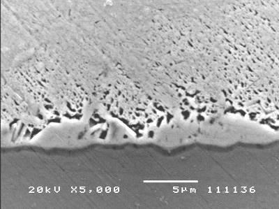
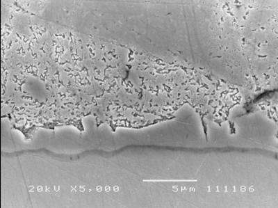
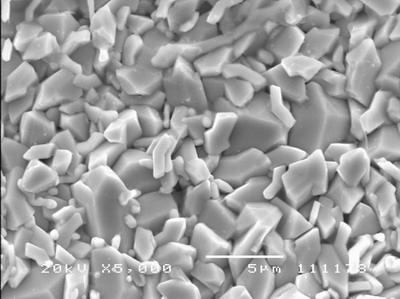
6 Ni 3 Sn 4 IMC grains are much bigger than the samples reflowed for only 30 s. IMC layer thickness also increases as compared to the IMC thickness of short time reflow samples, as shown in Fig. 1. The three types of morphology mentioned above still can be observed in all samples, but the boomerang-type and chunk-type morphology become the dominant shapes. When cooling rate decreases, total area occupied by chunk-type and boomerang-type grains increases and the grain size also increases. This means that the IMC grains grow bigger when the cooling rate slows down. From the cross sectional SEM micrographs, IMC thickness increases when the cooling rate reduces. Fig. 3 shows the same set of SEM micrographs reflowed at 251 o C for 600 s, followed by the three cooling rates. At this reflow time, majority Ni 3 Sn 4 IMC grains are in the shape of chunk-type with the grain size much bigger than the ones under shorter reflow time. From the top view SEM micrographs, there is not much difference in the IMC morphology among samples cooled in different rate. From the cross sectional SEM micrographs, it is clear that IMC thickness is greater when the cooling rate is slower. From the fast cooled sample in Fig. 3(a), the surfaces of the Ni 3 Sn 4 grains are covered with some white dots. These dots were identified as Ag 3 Sn and were not found in the samples with slower cooling rate. Its formation mechanism will be discussed elsewhere Effect of the cooling rate on Ni 3 Sn 4 IMC growth during liquid state reaction Average thickness of Ni 3 Sn 4 intermetallic compounds formed under different cooling rates and reflow time between Sn-3.5Ag solder and Ni-P UBM was measured. The relation of the thickness, reflow time and cooling rate is plotted in Fig. 4. The thickness of Ni 3 Sn 4 IMC layer - 5 -
7 ion general increases with decreasing cooling rate. Reflowing for 30 s, Ni 3 Sn 4 IMC thickness increases by 113% from fast cooling to slow cooling. For 180 s and 600 s reflow, this increase reduces to 61% and 44% respectively. This shows that at short holding time, IMC growth is more sensitive to post-reflow cooling rate. At the same cooling condition, the IMC thickness increases with reflow time. When reflow time extends from 30 s to 600 s, IMC thickness increases by 187% at fast cooling rate, 158% at medium cooling rate and 98% at slow cooling rate Effect of the cooling rate on Ni 3 Sn 4 IMC growth during annealing Sn-3.5Ag samples reflowed for 180 s and cooled under different cooling rates were annealed at 150 C and 170 o C. In all cases, IMC thickness increases with the extension of annealing time. Thickening kinetics of the Ni 3 Sn 4 IMC layer in solid state reaction between Sn-3.5Ag solder and Ni-P UBM are summarized in Fig. 5 and Fig. 6. The IMC growth kinetics constants are summarized in Table 1. The IMC thickness increases linearly with the square root of annealing time. This relation can be represented by = 0 + k t (1) where and 0 is the thickness of the IMC at time t and zero, respectively, and k the growth rate constant. This means that the IMC growth under thermal annealing is a diffusion-controlled process. Work by other researchers [1, 11, 13] on various soldering systems reached the same conclusion. For the Sn-3.5Ag/Ni-P system, it is not surprising that the k value at 170 o C is greater than that of 150 o C. However it is interesting to find that Ni 3 Sn 4 IMC in samples under fast cooling rate has larger growth constant k than that of slower cooling rate for the same aging - 6 -
8 condition. Explanation for this finding will be given later. 4. Discussion Post-reflow cooling rate affects the IMC formation at the cooling stage of a reflow process. High cooling rate favors nucleation but, since the holding time at high temperature zone is shorter, the effective time for IMC growth is shorter. This has resulted in the formation of a thin layer of fine grained IMCs. The reason why these fine grains are in needle shape has to do with the direct reaction between the Sn in the solder and the decomposed Ni from the metastable Ni-P UBM. With slow cooling rate, nucleation rate is lower but the IMC grains have enough time to grow. As a result, chunk type becomes dominant and the layer thickness is larger. With long time reflow, chunk-type grains form a continuous layer on UBM, as shown in Fig. 3(a), (c) and (e). Once this continuous IMC layer is formed, nucleation of new IMC grains becomes impossible. This is to compare with the case before the formation of a continuous layer when liquid solder exists in the grooves between neighboring IMC grains. Therefore even with fast cooling rate after long time reflow, needle type fine grains will not form. This work found that the IMC growth constant during annealing increases with the increase of post-reflow cooling rate. Chan et al. [14] made a similar observation for Cu-Sn intermetallic compounds. The explanation provided by them was that there existed some disordered regions inside solder alloy and this region increased with cooling rate. They proposed that the structure in these regions was more open and required lower diffusion activation energy. Therefore IMC growth rate of faster cooled solder joints would be larger than those of slower cooling. We believe that the continuous IMC layer during annealing is the limiting factor for - 7 -
9 further IMC growth. Therefore the microstructural difference in the IMC layer with different cooling rates should be responsible for the IMC growth rate difference. The IMC grain size in the sample with fast cooling rate is smaller than the one with slow cooling rate. More grain boundaries exist in the fine-grained IMC layer so that element diffusion is made easier. As a result, IMC grows to a higher thickness for the same annealing condition in high cooling rate samples. 5. Conclusions Needle-type, boomerang-type and chunk-type Ni 3 Sn 4 IMC grains are formed between Sn-3.5Ag solder and Ni-P UBM at different post-reflow cooling rate. When cooling rate decreases, the amount of needle-type grains also decreases, but the amount of chunk-type and boomerang-type grains increases due to grain growth and coalescence. The effect of cooling rate on IMC morphology is more eminent with shorter reflow time than longer time. After reflow for 600 s, the Ni 3 Sn 4 IMCs are in the same chunk-type morphology. IMC grain size is not affected by post-reflow cooling rate, either. During annealing process, the IMC growth has linear relation with square root of annealing time. The growth constant increases with samples undergoing high post-reflow cooling rate. This is believed to be due to the IMC microstructure difference under different cooling rates. Faster cooling rate forms finer IMC grains, and the elemental diffusion is made easy through grain boundaries
10 Acknowledgements This work was supported by an Academic Research Fund from Nanyang Technological University. Helpful discussion with Prof. Andriy Gusak from Cherkasy National University, Ukraine is gratefully acknowledged
11 References [1] K.N. Tu and K. Zeng, Materials Science and Engineering R34 (2001) 1. [2] J.W. Jang, P.G. Kim, and K.N. Tu, J. Appl. Phys. 85 (1999) [3] D.R. Frear and P.T. Vianco, Metallurgical and Materials Transactions A 25A (1994) [4] R.E. Pratt, E.I. Stromswold, and D.J. Quesnel, Journal of Electronic Materials 23 (1994) 375. [5] P.T. Vianco, Soldering Handbook 3rd Edition, American Welding Society, Miami FL, [6] K.S. Kim, S.H. Huh, and Suganuma K., Materials Science and Engineering A 333 (2002) 106. [7] J.G. Lee, F. Guo, S. Choi, K.N. Subramanian, T.R. Bieler, and J.P. Lucas, Journal of Electronic Materials 31 (2002) 946. [8] K. Noguchi, M. Ikeda, I. Shimizu, Y. Kawamura, and Y. Ohno, Materials Transactions 42 (2001) 761. [9] S.H. Fan, Y.C. Chan, C.W. Tang, and J.K.L. Lai, IEEE Transactions on Advanced Packaging 24 (2001) 10. [10] G.J. Qi, M. He and Z. Chen, Proceedings of Yazawa International Symposium, in Conjunction with the 132nd TMS Annual Meeting and Exhibition, March 2 6, 2003, San Diego, U.S.A., [11] S. Ahat, M. Sheng and L. Luo, J. Mater. Res. 16 (2001) [12] J.W. Jang, D.R. Frear, T.Y. Lee and K.N. Tu, J. Appl. Phys. 88 (2000) [13] D. Gur and M. Bamberger, Acta Mater. 46 (1998) [14] Y.C. Chan, S.H. Fan, and J.K.L. Lai, Journal of Electronic Packaging 125 (2003)
12 List of table Table 1 Calculated growth constants k (μm/h 1/2 ) of Ni 3 Sn 4 in annealing condition
13 List of figures Figure. 1 Morphology of Ni 3 Sn 4 IMC in Sn-3.5Ag/Ni-P samples reflowed for 30s then cooled in different cooling rates. (a) Fast cooling rate top structure, (b) Fast cooling rate cross section, (c) Medium cooling rate top structure, (d) Medium cooling rate cross section, (e) Slow cooling rate top structure, (f) Slow cooling rate cross section. Figure. 2 Morphology of Ni3Sn4 IMC in Sn-3.5Ag/Ni-P samples reflowed for 180s then cooled in different cooling rates. (a) Fast cooling rate top structure, (b) Fast cooling rate cross section, (c) Medium cooling rate top structure, (d) Medium cooling rate cross section, (e) Slow cooling rate top structure, (f) Slow cooling rate cross section. Figure. 3 Morphology of Ni3Sn4 IMC in Sn-3.5Ag/Ni-P samples reflowed for 600s then cooled in different cooling rates. (a) Fast cooling rate top structure, (b) Fast cooling rate cross section, (c) Medium cooling rate top structure, (d) Medium cooling rate cross section, (e) Slow cooling rate top structure, (f) Slow cooling rate cross section. Figure. 4 Thickness of Ni3Sn4 layer formed by reflowing Sn-3.5Ag solder on Ni-P UBM for different time and cooling in different rates. Figure. 5 Figure. 6 Ni3Sn4 IMC thickening kinetics in Sn-3.5Ag/Ni-P system annealed at 150oC. Ni3Sn4 IMC thickening kinetics in Sn-3.5Ag/Ni-P system annealed at 170oC
14 Cooling rate Fast Medium Slow Sn-3.5Ag, 170 o C Sn-3.5Ag, 150 o C Table
 - 14")
15 (a) (b) (c)
")

16 (d) (e) (f) Figure
 - 16")
17 (a) (b) (c)
")

18 (d) (e) (f) Figure
 - 18")
19 (a) (b) (c)
")

20 (d) (e) (f) Figure
21 Figure
22 Figure
23 Figure