MAKING SOLAR ELECTRICITY A USER-CONVENIENT REALITY WITH LIGHT MANAGEMENT
|
|
|
- Alison Long
- 5 years ago
- Views:
Transcription


1 1 MAKING SOLAR ELECTRICITY A USER-CONVENIENT REALITY WITH LIGHT MANAGEMENT IN PHOTOVOLTAICS Manuel J. Mendes, Olalla S. Sobrado, Sirazul Haque, Andreia Araújo, António Vicente, Tiago Mateus, Hugo Águas, Elvira Fortunato, Rodrigo Martins 2 Julho 2018 Encontro Ciência i3n/cenimat, Department of Materials Science, Faculty of Science and Technology, Universidade NOVA de Lisboa and CEMOP/UNINOVA, Campus de Caparica, Caparica, Portugal.

2 Perez et al. 2009, "A Fundamental Look At Energy Reserves For The Planet" Photovoltaics our future main energy 2


3 New market for PV consumer electronics 3
 Paper with")
 PECVD process H. Águas et al., Adv. Funct. Mater.")
4 Solar cells on Paper-based substrates 4 4-5% efficient cells for indoor solarpowered intelligent packaging deposited on: Liquid Packaging Cardboard (LPC) Paper with hydrophilic mesoporous (HM) surface Paper planarized with Cellullose-based films (EC) Optimized low-temperature (<150ºC) PECVD process H. Águas et al., Adv. Funct. Mater. (2015)


5 Solution for High-Efficient Thin-film PV 5 Lower material costs thicknesses on the order of mm No epitaxial constraints - infinite material possibilities Flexibility fabrication in roll-toroll processes and easier implementation in a broad-range of consumer-oriented applications
6 ~1mm Absorption issues of Thin-Film PV 6 UV VIS Near-Infrared

7 ~1mm Absorption issues of Thin-Film PV 7 UV VIS Near-Infrared NIR is poorly absorbed and corresponds to almost 50% of the solar spectrum!

 Issues: features cause dislocations")
8 ~1mm Mandatory solution: Light Trapping 8 Conventional Light Trapping techniques: Surface Texturing M. Despeisse et al., Phys. Status Solidi A (2011) Issues: features cause dislocations & cracks in PV material Electrical deterioration

9 Light management with Wave-optics 9 Photonic features: Wavelength-sized high-index dielectric (e.g. TiO 2 ) Best location: on front TCO contact Why? 1. Suppress reflection - efficient broadband ARCs 2. Adaptable forward scattered near-field which can focus light in distinct types of thin-film PV absorbers 3. Pronounced scattering cross sections which boost the optical path length of longer wavelength photons 4. Wide angular acceptance (compared with ARCs)


10 Optimization of Photonic Microstructures 10 Planar absorber layer LT structures should not increase the surface area of PV layer, to prevent increase of recombination Maximization of absorption in Si layer with Lumerical FDTD. Figure of merit = J SC M. J. Mendes et al., Nano Energy (2016)


11 Optimization of Photonic Microstructures 11 Planar absorber layer LT structures should not increase the surface area of PV layer, to prevent increase of recombination Maximization of absorption in Si layer with Lumerical FDTD. Figure of merit = J SC M. J. Mendes et al., iscience (2018)
")

12 Photocurrent (and efficiency) enhancement 12 M. J. Mendes et al., iscience (2018)
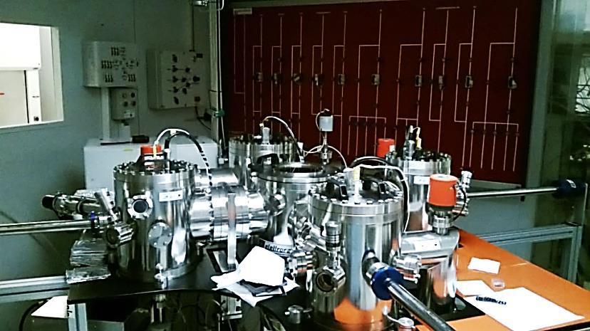

13 13 Photonic-enhanced Thin-film Si PV Spider-configuration multi-chamber Electrorava PECVD


14 Fabrication by Colloidal Lithography 14 Step 1: Deposition of 1-2 mm spheres in close-packed array Uniform structure over arbitrarily large area Step 2: Modification of shape and distance with dry-etching (RIE) Step 3: Infiltration of TiO 2 deposited with Sputtering 1 mm Step 4: Spheres removal (lift-off)


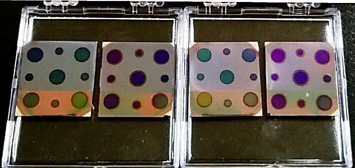
15 Implementation on Thin Film Si Solar Cells 15 O. S. Sobrado et al., JMC C (2017)


16 Opto-electronic response of nip a-si:h cells 16
, under projects POCI-01-0145-FEDER-007688")
17 THANK YOU! Any Questions? 17 Acknowledgements: FEDER funds, through the COMPETE 2020 Program, and national 17 funds, through Portuguese Foundation for Science and Technology (FCT-MEC), under projects POCI FEDER (UID/CTM/50025) and ALTALUZ (PTDC/CTM-ENE/5125/2014). Partial funding from EU projects BET-EU (H2020-TWINN-2015, grant ) and 1D-NEON (H2020-NMP-2015, grant ). M. J. M. also acknowledges FCT-MEC through grant SFRH/BPD/115566/2016. Advertisement: Need to hire a Post-Doc researcher to work in the field of Perovskite solar cells and light management 30-month contract, starting in October 2018

 due to TCO layer between structures &")
18 Opto-electronic improvement in a-si:h solar cells 18 TiO 2 front structures IZO front structures Scattering enhances photocurrent in visible and NIR range via path length amplification Anti-reflection is not high (UV-Vis range) due to TCO layer between structures & absorber
19 19 Extra slides


20 Trends in Photovoltaics 20 Current Leader: Current Research: Crystalline Si wafer-based solar cells Thin-film wafer-free cells High efficiency thin film cells enhanced by nanostructured materials and light management Epitaxially-grown III-V multijunction cells


21 Efficiency h (%) Tandem Solar Cells 21 A. Luque & A. Martí Phys. Rev. Lett. 78 (1997) 63.2 % E L E H Shockley & Queisser J. Appl. Phys. 32 (1961)


22 Solar Cell Efficiency Records 22 Zoom in NREL Efficiency chart:

23 Portrait of Light trapping effects 23 Cone-like shape indexmatching with high-index Si layer Multiple reflections of light with long penetration depth Fabry-Perot interference Forwardscattered nearfield light focusing in the thin layer Strong scattering cross-sections path lenght enhancement and confined waveguided modes M. J. Mendes et al. Nano Energy (2016)


24 Step 1 : Close-Packed Arrays of PS Spheres 24 Particles: 1-2 mm Polystyrene colloidal spheres Methodologies tested: Doctor Blade and Langmuir-Blodgett


25 Step 2 : Shaping colloidal mask with RIE 25 No etching 120 s RIE 160 s RIE


26 26 Step 3 : Infiltration of TiO 2

 27")


27 Step 4 : Litf-off of Spheres (mask) 27 Structures height: nm Spacing ~ 1 mm


28 Comparison with FDTD simulations 28 O. Sanchez-Sobrado, et al. J. Mat. Chem. C, 2017
 8.84 10.43 10.74 10.4 10.53 Fill Factor 57 % 54 % 53 % 56 % 54 % V OC (V) 0.87 0.87 0.87 0.86 0.")
29 Opto-electronic response of nip a-si:h cells 29 Planar REF TiO 2 (1.6 mm) TiO 2 (1.3 mm) IZO (1.6 mm) IZO (1.3 mm) Efficiency 4.37 % 4.83 % 4.94 % 5 % 4.89 % J SC (ma/cm 3 ) Fill Factor 57 % 54 % 53 % 56 % 54 % V OC (V)
30 The concept 4-T double-junctions 30 1) No current matching required 2) No lattice matching required 3) Distinct materials can be used for subcells. Big number of possible combinations! 4) Subcells optimized independently (e.g. in distinct labs) to get the most out of each 5) Facilitates implementation of light management structures T. P. White et al. IEEE PV (2014) 6) Allows better performance (adaptability) with changing illumination spectrum
 Efficiencies > 25% are feasible with current")
31 4-T double-junctions with c-si bottom cell 31 N. N. Lal et al. IEEE PV (2014) Efficiencies > 25% are feasible with current technology

32 32 Scientific Novelties of AltaLuz