National Kaohsiung First University of Sci. & Tech. LIGA. MicroSystem Fabrication Lab.
|
|
|
- Angel Booker
- 5 years ago
- Views:
Transcription
1 National Kaohsiung First University of Sci. & Tech. LIGA 李 立 MicroSystem Fabrication Lab.
2 錄 (thick PR) SU-8 JSR THB-430N LIGA LIGA-like 2


3 Nano- and micro molding provides a feasible way to the mass production of MEMS components/devices. Examples of MEMS devices: pumps, turbines, valves, fiber-optic connectors, micro-optics, gears, MEMS packaging, biomedical devices, etc. micro-lens (Heckele et al., 1998) LIGA toothed wheel (Ruprecht et al., 1997) Polymer micro mixer (Protron Mikrotechnik) 3

4 4

5 SU-8 參數 MicroChem SU-8 resist 5

6 SU-8 參數 (continue) 6
7 Fabrication of micromolds using SU-8 Aluminum is evaporated on the wafer. 220 µm SU-8 is spun, prebaked, exposed, and then postbaked. The steps are repeated for a 450-µm 2nd layer of SU-8. Develop the resist in a solvent. Evaporate a conductive layer on the SU-8 structure. Perform the electroplating. By dissolution of the Al-sacrificial layer, the micromold is separated from the wafer. The micromold is polished, and aligned with the upper and lower injection plate. Conduct the injection molding. 7


8 SU-8 Structure, metallic micromold, and injected component 8
, and glycerol ( ) filled process")
9 Diffraction ( ) Elimination Fabrication comparison of SU-8 standard process (left), and glycerol ( ) filled process (right). 9
 with a 100 µm air gap")
 Glycerol filling")
10 SU-8 photoresist exposure (a) with a 100 µm air gap between resist and mask (b) Glycerol filling process 10
 is to ensure good structure definition, and to stop the bottom SU-8 from mixing with the upper layer.")
11 Spin-on of CK-6020L resist, and anti-reflection coating for UV light absorption. Spin-coat the SU-8 resist, and expose to UV light Top wall thickness is controlled by exposure dosage. PEB (post exposure bake) is to ensure good structure definition, and to stop the bottom SU-8 from mixing with the upper layer. Release by the developing process Fabrication process of stacked channels 11

12 Top wall thickness controlled by different UV dosage. 12

13 Top wall thickness controlled Wall thickness vs. UV exposure dosage Fabricated stacked SU-8 buried Channels by UV dosage control 13
14 Micro-channel Fabrication Process A. PR Spin Coating SU8 Si Mask B. PR Exposure & Development C. Curing PDMS PDMS D. Drilling & O 2 Plasma Pasting PDMS glass 14

15 Rapid Prototyping of Complex 3-Dimensional Microfluidic Systems in PDMS (Anderson et al., 2002) 15
16 Motivation: JSR THB-430N Negative Resist To use JSR THB-430N negative tone resist (1.4 mm thick and aspect ratio at least 8) to replace SU-8 resist (2.1 mm and AR 18, usually less than 10) for ultra-thick-plating-mold fabrication. Problem for using SU-8: hard to strip O 2 plasma: slow etching rate; NMP stripper: corner cracking and resist swelling. 16
 Cracks appear on the")

17 Micro-gear structures fabricated by SU-8 and THB-430N resist (a) Cracks appear on the sharp corner of SU-8 structures (b) Same patterns by THB-430N with good structure integrity. 17
18 Spin thickness and soft bake properties of thick THB-430N resist Key #1: double-coating technique to achieve 1.4 mm PR thickness. (a) Resist thickness vs. spin rate (b) Resist weight vs. soft baking time 18
 The post exposure baking (PEB) procedure, commonly used in negative photoresist, e.")
19 Ti/Cu seed layer THB-430N is spun on the seed layer at 200 rpm. 2 nd layer of THB-430N is spun at 200 rpm to achieve 1.4-mm-thick PR. Then soft bake at 100 C for 7 hr. Exposed by UV-light, and then developed in THB-D1 developer for 1 hr with 40 KHz 26W ultrasonic agitation. Note: (1) The post exposure baking (PEB) procedure, commonly used in negative photoresist, e.g. SU-8, was not required in this process. (2) The developing time was 4 times shorter than that without ultrasound agitation. 2-step mold stripping: (1) acetone; (2) THB-S1 stripper at 70 C in 10 min. Fabrication process of ultrathick THB-430N resist 19
 Angle view of the gear structure (e) Top view of a close structure with cylinder shape; (f) Cross-section view of the close structure.")
20 Fabricated thick structures of THB-430N resist (a) (b) 66 µm thick coil mold; A close up of the coil mold (c) Top view of a 257 µm thick open structure with gear shape; (d) Angle view of the gear structure (e) Top view of a close structure with cylinder shape; (f) Cross-section view of the close structure. 20
 Top view Inclined view 15 µm 120 µm 40 µm 173")
21 THB-430N high aspect ratio open structure (aspect ratio~8) THB-430N high aspect ratio close structure (aspect ratio~4) Top view Inclined view 15 µm 120 µm 40 µm 173 µm 21


22 The effect of ultrasonic agitation 0.7 mm microstructure formed by THB 430N negative resist: without ultrasonic agitation with ultrasonic agitation 22
23 LIGA LIGA Lithographi (lithography, ) Galvanoformung (electroforming, ) Abformung (molding, ) 23
24 LIG LIGA 1975 年, Romankiw IBM X-ray 度 20µm 金 LIGA 1982 年, W. Ehrfeld Karlsruche Nuclear Research Center (Kernforschungszentrum Karlsruhe, KfK) 了 料 離 Wisconsin Guckel LIGA LIGA 24
25 High Aspect Ratio Molding - LIGA or UV-LIGA LIGA X-ray lithography, Expensive Fabrication of a LIGA mold insert: (modified from Hagmann et al., 1987) A. PR Spin Coating & X-ray Exposure X-ray B. PR Development Mask Photoresist Intermediate layer Si UV- LIGA: use UV light as the exposure source. C. Electroforming Metal (e.g., Ni) D. Seperation 25
 D. Remove Photoresist 26")
26 High Aspect Ratio Techniques Deep Reactive Ion Etching (RIE) How the deep RIE work? neutral ion Photoresist Si Fabrication Process: A. PR Spin Coating & Exposure B. PR Development UV light Mask Photoresist Si C. Deep Reactive Ion Etching Vertical walls by deep silicon RIE etching (Advanced MicroSensors) D. Remove Photoresist 26
27 High aspect ratio micromachining techniques LIGA process: feature thick (up to 1 mm) and high aspect ratio (100:1) microstructures fabrication UV-LIGA process: feature thick (up to 500 µm) and high aspect ratio (20:1) microstructures fabrication based on SU-8 photoresist. Deep silicon reactive iron etching (Deep RIE): low costs, small structure dimensions (1 µm), high aspect ratios (30:1), and short processing periods. 27

28 LIGA 流 28
29 29

30 30

 affect the")
31 Hot Embossing ( ) Shen and Lin (2001) studied in the hot embossing micro-lens fabrication how the process conditions (e.g., processing pressure and temperature) affect the height and radius of curvature. 31
32 Hot Embossing ( ) Shen et al. (2002): investigate the effects of the process conditions (temp. & pressure) on the penetation height and radius of curvature for microlens. Temperature (deg C) Time (min) 32
33 Two principal components of MEMS: A sensing or actuating element and a signal transduction unit. MEMS as a microsensor ( ): Ex: Accelerometer, Acceleration Voltage Cantilever beam Capacitance sensing 33
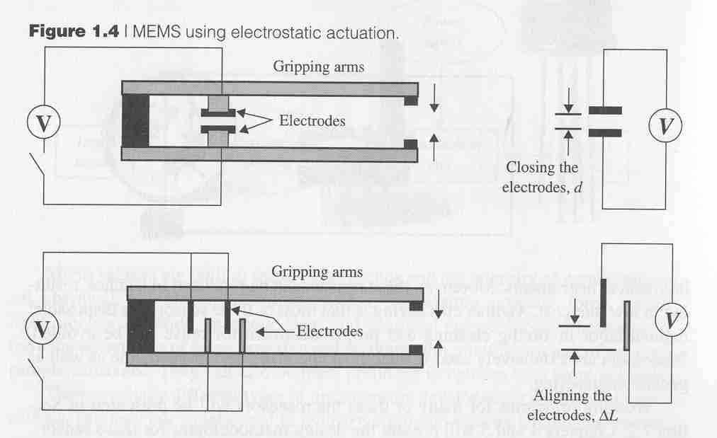
34 MEMS as a microactuator ( ): Ex.: Microgripper Displacement Mechanism Electrostatic Force 34

35 35
36 Microsystems: A microsystem is an engineering system that contains MEMS components that are designed to perform specific engineering functions. 3 components (Madou, 1997): micro sensors, actuators, and a processing unit. Example: an airbag deployment system 36
 for laserbeam scanning")
37 Laser Scanning Systems ( ) Electrostatic combdrive-actuated micromirrors ( ) for laserbeam scanning (e.g., bar-code scan) and positioning 37

38 DLP (Digital Light Processing) DLP 數 理 年 數 良 流 亮度 更 DLP 理 DMD 不 度 38

39 Gyroscope ( 螺, ) 螺 (Geiger et al., 2002) 39
40 Knowledge required for Microsystem Design: 40
41 References H. Lorenz, M. Despont, P. Vettiger, P. Renaud, 1998, Fabrication of photoplastic high-aspect ratio microparts and micromolds using SU-8 UV resist, Microsystem Technologies, 4, pp Yun-Ju Chuang, Fan-Gang Tseng, Jen-Hau Cheng, and Wei-keng Lin, 2003, A Novel Fabrication Method Of Embedded Micro Channels by Using SU-8 Thick-Film Photoresist, Sensors and Actuators A, 103, pp Yun-Ju Chuang, Fan-Gang Tseng and Wei-Keng Lin, 2002, Reduction of Diffraction Effect of UV Exposure On Su-8 Negative Thick Photoresist By Air Gap Elimination, paper submitted to Microsystem Technologies 8, pp Fan-Gang Tseng, and Chih-Sheng Yu, 2002, High Aspect Ratio Ultrathick Micro-Stencil by JSR THB-430N Negative UV Photoresist, Sensors and Actuators A, pp Fan-Gang Tseng, and Chih-Sheng Yu, 2002, Angle Effect of Ultrasonic Agitation On The Development Of Thick JSR THB-430n Negative UV Photoresist, Microsystem Technologies 8, pp X.-J. Shen, Li-Wei Pan and Liwei Lin, "Microplastic Embossing Process: Experimental and Theoretical Characterizations," Sensors and Actuators, Vol. A 97-98, pp , Geiger, W., Butt, W.U., Gaißer, A., Frech, J., Braxmaier, M., Link, T., Kohne, A., Nommensen, P., Sandmaier, H., Lang, W., and Sandmaier, H., 2002, Decoupled microgyros and the design principle DAVED, Sensors and Actuators A: Physical, vol. 95, pp Hsu, Tai-Ran, MEMS & Microsystems Design and Manufacturing, McGraw-Hill,